Characterization of electrical conductivity of porous metal fiber ...
Characterization of electrical conductivity of porous metal fiber ...
Characterization of electrical conductivity of porous metal fiber ...

Create successful ePaper yourself
Turn your PDF publications into a flip-book with our unique Google optimized e-Paper software.
Materials and Design 37 (2012) 161–165Contents lists available at SciVerse ScienceDirectMaterials and Designjournal homepage: www.elsevier.com/locate/matdes<strong>Characterization</strong> <strong>of</strong> <strong>electrical</strong> <strong>conductivity</strong> <strong>of</strong> <strong>porous</strong> <strong>metal</strong> <strong>fiber</strong> sintered sheetusing four-point probe methodWei Zhou a,b,⇑ , Yong Tang b , Rong Song a , Lelun Jiang a , K.S. Hui c , K.N. Hui da School <strong>of</strong> Engineering, Sun Yat-sen University, Guangzhou 510006, Chinab School <strong>of</strong> Mechanical and Automotive Engineering, South China University <strong>of</strong> Technology, Guangzhou 510640, Chinac Department <strong>of</strong> Systems Engineering and Engineering Management, City University <strong>of</strong> Hong Kong, Hong Kongd Department <strong>of</strong> Materials Science and Engineering, Pusan National University, Republic <strong>of</strong> KoreaarticleinfoabstractArticle history:Received 18 October 2011Accepted 29 December 2011Available online 5 January 2012Keywords:B. Fibers and filamentsC. SinteringE. Electrical propertiesNovel <strong>porous</strong> <strong>metal</strong> <strong>fiber</strong> sintered sheets (PMFSSs) with different porosities were fabricated by sinteringcopper <strong>fiber</strong>s. Using four-point probe method, comparative study was conducted to investigate the effects<strong>of</strong> probe spacing, porosity, and sintering condition on the <strong>electrical</strong> <strong>conductivity</strong> <strong>of</strong> PMFSS. Our experimentalresults showed that probe spacing plays an important role in determining the <strong>electrical</strong> <strong>conductivity</strong>.Uniform probe spacing was adopted in order to reduce the error caused by non-uniformity <strong>of</strong> probe spacing.The measured <strong>electrical</strong> <strong>conductivity</strong> was found to decrease with increasing porosity ranging from70% to 90% for the PMFSS produced under the same sintering condition. Our experimental results werefound to agree well with the theoretical prediction by Liu’s model for the PMFSS with different porosities.The effect <strong>of</strong> sintering condition on <strong>electrical</strong> <strong>conductivity</strong> was also investigated. It was revealed thathigher sintering temperature or longer holding time yields higher <strong>electrical</strong> <strong>conductivity</strong> <strong>of</strong> PMFSS.Ó 2012 Elsevier Ltd. All rights reserved.1. IntroductionPorous <strong>metal</strong>s, as a type <strong>of</strong> structural and functional materials,have been developing rapidly in recent years [1,2]. Porous <strong>metal</strong><strong>fiber</strong> sintered sheet (PMFSS), a relatively new group <strong>of</strong> <strong>porous</strong><strong>metal</strong>s have a three-dimensional reticulated structure featuringhigh porosity and large specific surface area. So far, PMFSS hasexhibited many significant engineering applications particularlyin defense and military industry, petrochemical industry, <strong>metal</strong>lurgicalmachinery, automotive industry, and environmental protectionfor its excellent performance in filtration and separation [1],fluid distribution [3], energy absorption [4], biomedical device[5], catalytic reaction [6], and thermal management [7]. Especially,PMFSS has been attracting attentions as a promising electrodematerial for high efficiency batteries [8–10]. Therefore, the <strong>electrical</strong><strong>conductivity</strong> is one <strong>of</strong> the most important properties need to beconsidered. However, previous research work mainly focused onthe open-celled and close-celled <strong>metal</strong> foams [11–13]. For PMFSSwith high porosity, limited information has been reported aboutthe relationships between microscopic structures and <strong>electrical</strong>properties. Characterizing the <strong>electrical</strong> <strong>conductivity</strong> <strong>of</strong> PMFSS isdemanding especially for its optimal performance in electrodeapplications.⇑ Corresponding author at: School <strong>of</strong> Engineering, Sun Yat-sen University,Guangzhou 510006, China. Tel./fax: +86 20 39332148.E-mail addresses: zhouw23@mail.sysu.edu.cn, abczhoulin@163.com (W. Zhou).With the development <strong>of</strong> science and technology as well aseconomy, the demand for <strong>porous</strong> <strong>metal</strong>s with high porosity and<strong>electrical</strong> properties is increasing. Some experimental measurementshave been made for characterizing the <strong>electrical</strong> properties<strong>of</strong> <strong>porous</strong> <strong>metal</strong>s. Dharmasena and Wadley [14] measured the <strong>electrical</strong><strong>conductivity</strong> <strong>of</strong> open-cell aluminum foam using four-pointprobe method. The experimental results <strong>of</strong> <strong>electrical</strong> <strong>conductivity</strong>confirmed the linear dependence upon density, but the slope wassmaller than that predicted by the unit-cell model. Goodall et al.[15] characterized the <strong>electrical</strong> <strong>conductivity</strong> <strong>of</strong> replicated openporemicrocellular <strong>metal</strong> over a wide range <strong>of</strong> relative densityusing four-point probe technique. It was found that the <strong>electrical</strong><strong>conductivity</strong> <strong>of</strong> <strong>metal</strong>lic foams varied strongly with differentporosities. Liu et al. [16–18] also conducted a series <strong>of</strong> experimentsto determine the <strong>electrical</strong> resistivity <strong>of</strong> nickel foams developed byelectroplating on the polyether sponge sheet using a double circuitbridge. Duan et al. [19] developed a methodology to calculate theapparent resistivity <strong>of</strong> <strong>metal</strong>lic foam based on the pentagonaldodecahedron model. The calculated evaluations based on thismethodology approximately agree with the experimental results<strong>of</strong> Ni–Cr foams and Ni foams. Recently, Cuevas et al. [20] reviewedthe experimental and theoretical works about the <strong>electrical</strong> <strong>conductivity</strong><strong>of</strong> <strong>metal</strong> foams. A new empirical formula was proposedto describe the relationship between porosity and <strong>electrical</strong> <strong>conductivity</strong>for different types <strong>of</strong> foams.From the above reported work, it is found that the detailedstudy <strong>of</strong> the relationships relating the porosity and sintering0261-3069/$ - see front matter Ó 2012 Elsevier Ltd. All rights reserved.doi:10.1016/j.matdes.2011.12.046
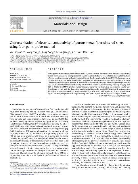
162 W. Zhou et al. / Materials and Design 37 (2012) 161–165condition with the <strong>electrical</strong> <strong>conductivity</strong> <strong>of</strong> PMFSS is lacking incurrent literature. In the present study, the PMFSS with a threedimensionalreticulated structure was fabricated through thesolid-state sintering <strong>of</strong> copper <strong>fiber</strong>s. Four-point probe methodwas used to investigate the dependences <strong>of</strong> <strong>electrical</strong> <strong>conductivity</strong><strong>of</strong> PMFSS on the probe spacing, porosity, sintering condition.2. Experimental procedures2.1. Manufacturing process <strong>of</strong> PMFSSAs reported previously [21], the processing procedure <strong>of</strong> PMFSSwas divided into five steps including <strong>fiber</strong> chipping, mold-pressing,sintering, cooling, and testing. First <strong>of</strong> all, the continuous copper<strong>fiber</strong>s were fabricated by cutting method with a multi-tooth tool.These copper <strong>fiber</strong>s were then cut into segments with length rangingfrom 10 to 20 mm. Next, the copper <strong>fiber</strong>s were randomly distributedinto the packing chamber <strong>of</strong> the mold pressing equipment.Then pressure was applied by screwing the bolt apparatus. In doingso, a semi-finished PMFSS with the same shape <strong>of</strong> the packingchamber was obtained. Sintering was then carried out in hydrogengas atmosphere with constant pressure <strong>of</strong> 0.3 MPa. Different sinteringtemperatures ranging from 700 °C to 1000 °C were taken.Stage heating method was used to optimize the heating rate, whichwas kept at 300 °C/h when the temperature was below 800 °C,while reduced to 200 °C/h as the temperature was above 800 °C.The holding time was set as either 30 min or 60 min. When the sinteringwas completed, the sample was removed from the furnaceand cooled to room temperature in air. Finally, the mold pressingequipment was disassembled and the PMFSS was ready for <strong>electrical</strong>characterization. The appearance <strong>of</strong> PMFSS produced by abovemanufacturing procedure was shown in Fig. 1.Since the obtained PMFSS has a regular geometric shape, we cancalculate the average porosity using the quality–volume methodformulated byhð%Þ ¼ 1MqV 100where V is the volume <strong>of</strong> PMFSS (cm 3 ), M, is the mass <strong>of</strong> PMFSS (g),and q is the density <strong>of</strong> red copper (g/cm 3 ).2.2. Electrical <strong>conductivity</strong> measurementsScanning electron microscopy (JSM-6380LA, Japan) wasadopted to observe the microscopic structure <strong>of</strong> PMFSS. Themeasurements <strong>of</strong> <strong>electrical</strong> <strong>conductivity</strong> were performed by fourpointprobe method in which four sharp probes are mechanicallyð1Þpressed on the testing sample surface, as shown in Fig. 2. An inlinefour-point probe was placed on the surface <strong>of</strong> the testing sample[14]. A constant current was applied through the outer currentprobes using constant current electric power (Xia Men MingweiElectricity CO., ITD, China, D-50D). The voltage drop across thetwo inner voltage probes was measured with a digital voltmeter(Agilent, USA, HP34401A). The <strong>electrical</strong> resistivity r is given by[14].2p V Ir ¼ h i ð2Þ1X 1þ 1 1 1X 3 X 1 þX 2 X 2 þX 3where X 1 , X 2 , and X 3 are the probe spacings shown in Fig. 2. The<strong>electrical</strong> <strong>conductivity</strong> r (in units <strong>of</strong> S/m) is expressed asr ¼ 1 rIn order to reduce the cell size effects and characterize the overall<strong>electrical</strong> behavior, the dimension <strong>of</strong> samples was taken as70 40 4 mm which was several times larger than the pore size[12]. In order to eliminate the polarization effect and potential <strong>of</strong>fset,voltage drop was measured under forward and reverse currentdirections and the average <strong>of</strong> the measured absolute values wascalculated [15,22]. For the specific porosity and sintering condition,ten specimens were prepared. Their mean value was taken as the<strong>electrical</strong> <strong>conductivity</strong> <strong>of</strong> PMFSS with such porosity and sinteringcondition. All measurements were performed in ambient conditionwith temperature approximately 25 °C.3. Results and discussion3.1. Microscopic observations <strong>of</strong> PMFSSBefore sintering, the copper <strong>fiber</strong>s were distributed randomly inthe pressing mold. The compression was then conducted to makecontact regions among <strong>fiber</strong>s.During sintering process, sintering joints were formed among<strong>fiber</strong>s as a result <strong>of</strong> material migration at elevated temperature.Fiber’s <strong>metal</strong>lurgy unification occurred, resulting in PMFSS with athree-dimensional reticulated structure [21]. Fig 3a shows the typicalthree-dimensional reticulated structure <strong>of</strong> PMFSS sintered at800 °C for 30 min. Such structure has been used as catalyst carrieras well as heat transfer medium in the last 3 years [23,24]. FromFig. 3b, we found that there were two types <strong>of</strong> sintering jointspresented in PMFSS including <strong>fiber</strong>-to-<strong>fiber</strong> surface contact andcrossing <strong>fiber</strong> meshing [21,25]. It was also noted that PMFSS couldhave a wide porosity range from 60% to 98%, large pore size, andinterconnected pores. Moreover, it is easily to find that copper<strong>fiber</strong>s have a large number <strong>of</strong> surface microstructures afterð3ÞE=70% E=80% E=90%IICurrent probe Voltage probes Current probeEquipotential surfacePMFSS SampleCurrent flow lineFig. 1. Appearance <strong>of</strong> PMFSS with different porosities produced by the solid-statesintering <strong>of</strong> copper <strong>fiber</strong>s.Fig. 2. Schematic diagram <strong>of</strong> four-point probe method for measuring the <strong>electrical</strong><strong>conductivity</strong> <strong>of</strong> PMFSS.
W. Zhou et al. / Materials and Design 37 (2012) 161–165 163(a)(b)(c)Fig. 3. SEM images <strong>of</strong> PMFSS produced by the solid-state sintering <strong>of</strong> copper <strong>fiber</strong>s: (a) three-dimensional reticulated structure <strong>of</strong> PMFSS sintered at 800 °C for 30 min, (b)SEM image <strong>of</strong> bonding types among <strong>fiber</strong>s in the PMFSS, and (c) surface microstructures <strong>of</strong> single copper <strong>fiber</strong> after sintering at 800 °C for 30 min.sintering at 800 °C for 30 min, as shown in Fig. 3c. When the sinteringtemperature was increased, a majority <strong>of</strong> the surface microstructuresdisappeared, giving rise to the smooth surface <strong>of</strong> the<strong>fiber</strong>s [21]. Therefore, the microscopic structures <strong>of</strong> PMFSSdepended on the sintering condition.3.2. Effect <strong>of</strong> probe spacing on the <strong>electrical</strong> <strong>conductivity</strong> <strong>of</strong> PMFSSTo analyze the effect <strong>of</strong> probe spacing on <strong>electrical</strong> <strong>conductivity</strong>,different probe spacings were adopted to measure the <strong>electrical</strong><strong>conductivity</strong> <strong>of</strong> PMFSS with porosity <strong>of</strong> 90% sintered at 800 °C for30 min. In this study, four sets <strong>of</strong> probe spacing were selectedincluding set A (X 1 = X 2 = X 3 = 70/3 mm), set B (X 1 = X 3 = 20 mm,X 2 = 30 mm), set C (X 1 = 15 mm, X 2 = 25 mm, X 3 = 30 mm), and setD(X 1 = X 2 = X 3 = 15 mm). The measured <strong>electrical</strong> <strong>conductivity</strong> <strong>of</strong>PMFSS using different probe spacings is shown in Fig. 4. It wasobserved that set A and set D exhibited similar <strong>electrical</strong> <strong>conductivity</strong>plots. However, set B and C showed the increase <strong>of</strong> <strong>electrical</strong><strong>conductivity</strong>. Thus, uniform probe spacing was adopted to measurethe <strong>electrical</strong> <strong>conductivity</strong> <strong>of</strong> PMFSS. Moreover, the <strong>electrical</strong> <strong>conductivity</strong><strong>of</strong> PMFSS was found to decrease with increasing inputvoltage. This can be attributed to the increase <strong>of</strong> temperaturecaused by higher input voltage [26]. Besides, the average values<strong>of</strong> the measurements with different probe spacings are shown inFig. 5. It was found that the average values <strong>of</strong> <strong>electrical</strong> <strong>conductivity</strong>were little lower than that <strong>of</strong> the <strong>metal</strong> foam with same porosity <strong>of</strong>6S/mElectrical <strong>conductivity</strong>0.120.110.100.090.080.070.060.05Probe spacing AProbe spacing BProbe spacing CProbe spacing D0.0 0.2 0.4 0.6 0.8 1.0Voltage (mV)Fig. 4. Measured <strong>electrical</strong> <strong>conductivity</strong> <strong>of</strong> PMFSS using different probe spacings.6 S/mAverage <strong>electrical</strong> <strong>conductivity</strong>0.120.100.080.060.040.020.055A0.0850.063BCProbe spacings0.056Fig. 5. Average measured <strong>electrical</strong> <strong>conductivity</strong> <strong>of</strong> PMFSS using different probespacings.90% [11,14]. Also, the approximate average values <strong>of</strong> <strong>electrical</strong><strong>conductivity</strong> were found when the uniform probe spacing was selected.In the following section, uniform probe spacing <strong>of</strong> set Awas taken to measure the <strong>electrical</strong> <strong>conductivity</strong> <strong>of</strong> PMFSS.3.3. Effect <strong>of</strong> porosity on the <strong>electrical</strong> <strong>conductivity</strong> <strong>of</strong> PMFSSPorosity is the most characteristic feature <strong>of</strong> <strong>porous</strong> materials.So far, several models have been proposed to bridge the relationshipbetween <strong>electrical</strong> <strong>conductivity</strong> and porosity for <strong>porous</strong> <strong>metal</strong>s,which can help to improve the design <strong>of</strong> the materials. Forinstance, after measuring the <strong>electrical</strong> <strong>conductivity</strong> <strong>of</strong> Ni foamproduced by <strong>metal</strong> deposition techniques, Langlois and Coeuret[27] firstly proposed a half-empirical formula relating the <strong>electrical</strong><strong>conductivity</strong> and the porosity for <strong>porous</strong> material with high porosityranging from 97% to 97.8% as follows:r ¼ 1 h4 r 0 ð4Þwhere r and r 0 are the <strong>electrical</strong> <strong>conductivity</strong> <strong>of</strong> the <strong>porous</strong> andcompact <strong>metal</strong>s, respectively, and h stands for the porosity.Eq. (4) is obtained from only a few experiments based on thenickel foams. Taking the differences <strong>of</strong> the specific manufacturingprocesses into account, the formula was revised to be [16].D