AUO Confidential For PROMATE Internal Use Only / 2011/8/16
AUO Confidential For PROMATE Internal Use Only / 2011/8/16
AUO Confidential For PROMATE Internal Use Only / 2011/8/16

You also want an ePaper? Increase the reach of your titles
YUMPU automatically turns print PDFs into web optimized ePapers that Google loves.
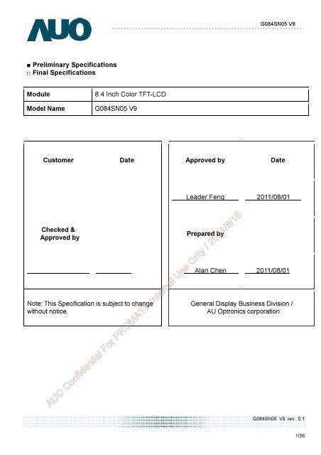
■ Preliminary Specifications<br />
□ Final Specifications<br />
Module 8.4 Inch Color TFT-LCD<br />
Model Name G084SN05 V9<br />
Customer Date<br />
Checked &<br />
Approved by<br />
Note: This Specification is subject to change<br />
without notice.<br />
G084SN05 V9<br />
Approved by Date<br />
Leader Feng <strong>2011</strong>/08/01<br />
Prepared by<br />
Alan Chen <strong>2011</strong>/08/01<br />
General Display Business Division /<br />
AU Optronics corporation<br />
<strong>AUO</strong> <strong>Confidential</strong> <strong>For</strong> <strong>PROMATE</strong> <strong>Internal</strong> <strong>Use</strong> <strong>Only</strong> / <strong>2011</strong>/8/<strong>16</strong><br />
G084SN05 V9 rev. 0.1<br />
1/26
G084SN05 V9<br />
Contents<br />
1. Operating Precautions.....................................................................................4<br />
2. General Description.........................................................................................5<br />
2.1 Display Characteristics...........................................................................................................5<br />
2.2 Optical Characteristics ...........................................................................................................6<br />
3. Functional Block Diagram ...............................................................................9<br />
4. Absolute Maximum Ratings ..........................................................................10<br />
4.1 Absolute Ratings of TFT LCD Module .................................................................................10<br />
4.2 Absolute Ratings of Environment ........................................................................................10<br />
5. Electrical Characteristics ..............................................................................11<br />
5.1 TFT LCD Module ..................................................................................................................11<br />
5.2 Backlight Unit........................................................................................................................13<br />
6. Signal Characteristic .....................................................................................14<br />
6.1 Pixel <strong>For</strong>mat Image ..............................................................................................................14<br />
6.2 Signal Description ................................................................................................................15<br />
6.3 Scanning Direction ...............................................................................................................<strong>16</strong><br />
6.4 The Input Data <strong>For</strong>mat .........................................................................................................17<br />
6.5 Interface Timing....................................................................................................................18<br />
6.6 Power ON/OFF Sequence...................................................................................................19<br />
7. Connector & Pin Assignment........................................................................21<br />
7.1 TFT LCD Signal (CN1): LVDS Connector ...........................................................................21<br />
7.2 LED Backlight Unit (CN2): LED Driver Connector ..............................................................21<br />
7.3 LED Light Bar Input Connector (CN3):................................................................................22<br />
8. Reliability Test Criteria ..................................................................................22<br />
9. Mechanical Characteristics ...........................................................................23<br />
9.1 LCM Front View....................................................................................................................23<br />
9.2 LCM Rear View ....................................................................................................................24<br />
10. Label and Packaging....................................................................................25<br />
10.1 Shipping Label (on the rear side of TFT-LCD display)......................................................25<br />
10.2 Carton Package .................................................................................................................25<br />
11 Safety.............................................................................................................26<br />
11.1 Sharp Edge Requirements.................................................................................................26<br />
11.2 Materials .............................................................................................................................26<br />
11.3 Capacitors...........................................................................................................................26<br />
11.4 National Test Lab Requirement..........................................................................................26<br />
<strong>AUO</strong> <strong>Confidential</strong> <strong>For</strong> <strong>PROMATE</strong> <strong>Internal</strong> <strong>Use</strong> <strong>Only</strong> / <strong>2011</strong>/8/<strong>16</strong><br />
G084SN05 V9 rev. 0.1<br />
2/26
Record of Revision<br />
Version and Date Page Old description New Description<br />
0.0 <strong>2011</strong>/04/07 First Edition<br />
0.1 <strong>2011</strong>.08/01 5 Update Input Voltage, Power<br />
Consumption, Weight<br />
6 Update Response Time<br />
11 Update Power Specification<br />
G084SN05 V9<br />
13 Update Parameter guideline for LED<br />
backlight<br />
20, 21 Update LED Connector, Cable Color<br />
<strong>AUO</strong> <strong>Confidential</strong> <strong>For</strong> <strong>PROMATE</strong> <strong>Internal</strong> <strong>Use</strong> <strong>Only</strong> / <strong>2011</strong>/8/<strong>16</strong><br />
G084SN05 V9 rev. 0.1<br />
3/26
1. Operating Precautions<br />
1) Since front polarizer is easily damaged, please be cautious not to scratch it.<br />
G084SN05 V9<br />
2) Be sure to turn off power supply when inserting or disconnecting from input connector.<br />
3) Wipe off water drop immediately. Long contact with water may cause discoloration or spots.<br />
4) When the panel surface is soiled, wipe it with absorbent cotton or soft cloth.<br />
5) Since the panel is made of glass, it may be broken or cracked if dropped or bumped on hard<br />
surface.<br />
6) To avoid ESD (Electro Static Discharde) damage, be sure to ground yourself before handling<br />
TFT-LCD Module.<br />
7) Do not open nor modify the module assembly.<br />
8) Do not press the reflector sheet at the back of the module to any direction.<br />
9) In case if a module has to be put back into the packing container slot after it was taken out<br />
from the container, do not press the center of the LED Reflector edge. Instead, press at the<br />
far ends of the LED Reflector edge softly. Otherwise the TFT Module may be damaged.<br />
10) At the insertion or removal of the Signal Interface Connector, be sure not to rotate nor tilt the<br />
Interface Connector of the TFT Module.<br />
11)After installation of the TFT Module into an enclosure (Notebook PC Bezel, for example), do<br />
not twist nor bend the TFT Module even momentary. At designing the enclosure, it should be<br />
taken into consideration that no bending/twisting forces are applied to the TFT Module from<br />
outside. Otherwise the TFT Module may be damaged.<br />
12) Small amount of materials having no flammability grade is used in the LCD module. The LCD<br />
module should be supplied by power complied with requirements of Limited Power Source<br />
(IEC60950 or UL1950), or be applied exemption.<br />
13) Severe temperature condition may result in different luminance, response time.<br />
14) Continuous operating TFT-LCD Module under high temperature environment may accelerate<br />
LED light bar exhaustion and reduce luminance dramatically.<br />
15) The data on this specification sheet is applicable when LCD module is placed in landscape<br />
position.<br />
<strong>16</strong>) Continuous displaying fixed pattern may induce image sticking. It is recommended to use<br />
screen saver or shuffle content periodically if fixed pattern is displayed on the screen.<br />
<strong>AUO</strong> <strong>Confidential</strong> <strong>For</strong> <strong>PROMATE</strong> <strong>Internal</strong> <strong>Use</strong> <strong>Only</strong> / <strong>2011</strong>/8/<strong>16</strong><br />
G084SN05 V9 rev. 0.1<br />
4/26
2. General Description<br />
This specification applies to the 8.4 inch color TFT LCD module G084SN05 V9.<br />
G084SN05 V9<br />
G084SN05 V9 designed with wide viewing angle; wide operating temperature and long life LEDs<br />
backlight is well suited to be the display units for Industrial Applications.<br />
LED driving board for backlight unit is included in this panel and the structure of the LED units is<br />
replaceable.<br />
G084SN05 V9 is built in timing controller and LVDS interface.<br />
The screen format is intended to support the SVGA (800(H) x 600(V)) screen and <strong>16</strong>.2M (RGB<br />
8-bits) or 262k colors (RGB 6-bits).<br />
G084SN05 V9 is a RoHS product.<br />
2.1 Display Characteristics<br />
The following items are characteristics summary on the table under 25 0C condition:<br />
Items Unit Specifications<br />
Screen Diagonal [inch] 8.4 ( 213.4mm )<br />
Active Area [mm] 170.4(H) x 127.8(V)<br />
Pixels H x V 800x3(RGB) x 600<br />
Pixel Pitch [mm] 0.213x 0.213<br />
Pixel Arrangement R.G.B. Vertical Stripe<br />
Display Mode TN, Normally White<br />
Nominal Input Voltage VDD [Volt] 3.3 (typ)<br />
Typical Power Consumption [Watt] 4.5 (typ)<br />
Weight [Grams] 250±10 (typ)<br />
Physical Size [mm] 203.0(W) x 142.5(H) x 8.0(D) (typ.)<br />
Electrical Interface 1 channel LVDS<br />
Surface Treatment Anti-glare, Hardness 3H<br />
Support Color 262K(6-bit) / <strong>16</strong>.2M(8-bit)<br />
Temperature Range<br />
Operating<br />
Storage (Non-Operating)<br />
[ o C]<br />
[ o C]<br />
RoHS Compliance RoHS Compliance<br />
-30 to +85 (panel surface temperature)<br />
-30 to +85<br />
<strong>AUO</strong> <strong>Confidential</strong> <strong>For</strong> <strong>PROMATE</strong> <strong>Internal</strong> <strong>Use</strong> <strong>Only</strong> / <strong>2011</strong>/8/<strong>16</strong><br />
G084SN05 V9 rev. 0.1<br />
5/26
2.2 Optical Characteristics<br />
The optical characteristics are measured under stable conditions at 250C (Room Temperature):<br />
G084SN05 V9<br />
Item Unit Conditions Min. Typ. Max. Note<br />
White Luminance [cd/m2]<br />
IF= 80mA<br />
(center point)<br />
TBD 450 - 1<br />
Uniformity % 9 Points TBD 75 - 1, 2, 3<br />
Contrast Ratio TBD 600 - 4<br />
Response Time<br />
Viewing Angle<br />
Color / Chromaticity<br />
Coordinates<br />
(CIE 1931)<br />
[msec] Rising - 20 TBD<br />
[msec] Falling - 10 TBD<br />
[msec] Raising + Falling - 30 TBD<br />
[degree]<br />
[degree]<br />
[degree]<br />
[degree]<br />
Horizontal (Right)<br />
CR 10 (Left)<br />
Vertical (Upper)<br />
CR 10 (Lower)<br />
TBD<br />
TBD<br />
80<br />
80<br />
80<br />
60<br />
Red x TBD TBD TBD<br />
Red y TBD TBD TBD<br />
Green x TBD TBD TBD<br />
Green y TBD TBD TBD<br />
Blue x TBD TBD TBD<br />
Blue y TBD TBD TBD<br />
White x 0.26 0.31 0.36<br />
White y 0.28 0.33 0.38<br />
Color Gamut % 45 - 1<br />
Note 1: Measurement method<br />
Equipment : Pattern Generator, Power Supply, Digital Voltmeter, Luminance meter (SR_3 or equivalent)<br />
Aperture 1<br />
Test Point Center with50cmviewingdistance<br />
Environment < 1 lux<br />
LCD Module<br />
Measuring distance<br />
Module Driving Equipment<br />
SR_3 or<br />
equivalent<br />
<strong>AUO</strong> <strong>Confidential</strong> <strong>For</strong> <strong>PROMATE</strong> <strong>Internal</strong> <strong>Use</strong> <strong>Only</strong> / <strong>2011</strong>/8/<strong>16</strong><br />
-<br />
-<br />
-<br />
-<br />
5<br />
6<br />
1<br />
G084SN05 V9 rev. 0.1<br />
6/26
Note 2: Definition of 9 points position (Display active area : 170.4(H) x 127.8(V))<br />
G084SN05 V9<br />
Note 3: The luminance uniformity of 9 points is defined by dividing the minimum luminance value by the maximum test<br />
point luminance<br />
Note 4: Definition of contrast ratio (CR):<br />
Note 5: Definition of response time:<br />
Contrast ratio (CR)=<br />
The output signals of photo detector are measured when the input signals are changed from “White” to “Black”<br />
(falling time) and from “Black” to “White” (rising time), respectively. The response time interval is between 10% and<br />
90% of amplitudes. Please refer to the figure as below.<br />
Optical<br />
response<br />
90 % 50 %<br />
%<br />
100<br />
90<br />
10<br />
0<br />
10 %<br />
Minimum Brightness of nine points<br />
δW9 = Maximum Brightness of nine points<br />
Brightness on the “White” state<br />
Brightness on the “Black” state<br />
10 %<br />
50 %<br />
90 %<br />
Tf Tr<br />
White Black White<br />
<strong>AUO</strong> <strong>Confidential</strong> <strong>For</strong> <strong>PROMATE</strong> <strong>Internal</strong> <strong>Use</strong> <strong>Only</strong> / <strong>2011</strong>/8/<strong>16</strong><br />
G084SN05 V9 rev. 0.1<br />
7/26
G084SN05 V9<br />
Note 6: Definition of viewing angle Viewingangleisthemeasurementofcontrastratio�10,athescrencenter,overa180°horizontaland180°<br />
vertical range (off-normal viewing angles). The 180° viewing angle range is broken down as below: 90° (θ) horizontal<br />
left and right, and 90° (Φ) vertical high (up) and low (down). The measurement direction is typically perpendicular to the<br />
display surface with the screen rotated to its center to develop the desired measurement viewing angle.<br />
<strong>AUO</strong> <strong>Confidential</strong> <strong>For</strong> <strong>PROMATE</strong> <strong>Internal</strong> <strong>Use</strong> <strong>Only</strong> / <strong>2011</strong>/8/<strong>16</strong><br />
G084SN05 V9 rev. 0.1<br />
8/26
3. Functional Block Diagram<br />
The following diagram shows the functional block of the 8.4 inch color TFT/LCD module:<br />
<strong>AUO</strong> <strong>Confidential</strong> <strong>For</strong> <strong>PROMATE</strong> <strong>Internal</strong> <strong>Use</strong> <strong>Only</strong> / <strong>2011</strong>/8/<strong>16</strong><br />
G084SN05 V9<br />
G084SN05 V9 rev. 0.1<br />
9/26
4. Absolute Maximum Ratings<br />
4.1 Absolute Ratings of TFT LCD Module<br />
G084SN05 V9<br />
Item Symbol Min Max Unit Conditions<br />
Logic/LCD Drive Voltage VDD -0.3 +3.6 [Volt]<br />
4.2 Absolute Ratings of Environment<br />
Item Symbol Min Max Unit<br />
Operating Temperature TOP -30 +85 [ o C]<br />
Operation Humidity HOP 5 90 [%RH]<br />
Storage Temperature TST -30 +85 [ o C]<br />
Storage Humidity HST 5 90 [%RH]<br />
Note: Maximum Wet-Bulb should be 390C and no condensation.<br />
<strong>AUO</strong> <strong>Confidential</strong> <strong>For</strong> <strong>PROMATE</strong> <strong>Internal</strong> <strong>Use</strong> <strong>Only</strong> / <strong>2011</strong>/8/<strong>16</strong><br />
G084SN05 V9 rev. 0.1<br />
10/26
5. Electrical Characteristics<br />
5.1 TFT LCD Module<br />
5.1.1 Power Specification<br />
Symbol Parameter Min Typ Max Units Remark<br />
VDD<br />
Logic/LCD Drive<br />
Voltage<br />
3.0 3.3 3.6 [Volt]<br />
±10%<br />
IVDD<br />
VDD Current - 270 330 [mA]<br />
64 Gray Bar Pattern<br />
(VDD=3.3V, at 60Hz)<br />
Irush LCD LCD Inrush Current - - 3 [A] Note 1<br />
64 Gray Bar Pattern<br />
PVDD VDD Power - 0.9 1.2 [Watt] (VDD=3.3V, at 60Hz)<br />
Note 1: Measurement condition:<br />
0V<br />
1 2<br />
SW1<br />
SW MAG-SPST<br />
(High to Low)<br />
Control<br />
Signal<br />
+12.0V<br />
10%<br />
C2<br />
1uF/25V<br />
R2<br />
1K<br />
90%<br />
+3.3V<br />
R1<br />
47K<br />
R2<br />
1K<br />
VR1<br />
47K<br />
470us<br />
VDD rising time<br />
C3<br />
G<br />
D6<br />
Q3<br />
AO6402<br />
D5<br />
D2 S<br />
D1<br />
D1<br />
D2<br />
D5<br />
D6<br />
S<br />
0.01uF/25V<br />
G<br />
Q3<br />
AO6402<br />
3.3V<br />
F1<br />
C1<br />
1uF/<strong>16</strong>V<br />
64 Gray pattern<br />
<strong>AUO</strong> <strong>Confidential</strong> <strong>For</strong> <strong>PROMATE</strong> <strong>Internal</strong> <strong>Use</strong> <strong>Only</strong> / <strong>2011</strong>/8/<strong>16</strong><br />
G084SN05 V9<br />
VDD<br />
VCC<br />
(LCD Module Input)<br />
G084SN05 V9 rev. 0.1<br />
11/26
5.1.2 Signal Electrical Characteristics<br />
Input signals shall be low or Hi-Z state when VDD is off.<br />
G084SN05 V9<br />
Symbol Item Min. Typ. Max. Unit Remark<br />
VTH Differential Input High Threshold - - 100 [mV] VICM=1.2V<br />
VTL Differential Input Low Threshold -100 - - [mV] VICM=1.2V<br />
|VID| Input Differential Voltage 100 400 600 [mV]<br />
VICM<br />
Differential Input Common Mode Voltage 1.1 1.6 [V] VTH/VTL=±100mV<br />
Note: LVDS Signal Waveform.<br />
VICM<br />
<strong>AUO</strong> <strong>Confidential</strong> <strong>For</strong> <strong>PROMATE</strong> <strong>Internal</strong> <strong>Use</strong> <strong>Only</strong> / <strong>2011</strong>/8/<strong>16</strong><br />
G084SN05 V9 rev. 0.1<br />
12/26
5.2 Backlight Unit<br />
5.2.1 Parameter guideline for LED backlight<br />
G084SN05 V9<br />
Following characteristics are measured under a stable condition using an inverter at 250C (Room Temperature):<br />
Symbol Parameter Min. Typ. Max. Unit Remark<br />
VCC Input Voltage 10.8 12 12.6<br />
IVCC Input Current - 0.30 -<br />
PVCC Power Consumption - 3.6 3.78<br />
Irush LED Inrush Current - - 0.68<br />
FPWM Dimming Frequency 200 - 20K<br />
Swing Voltage 3 3.3 5.5<br />
Dimming Duty Cycle 5 - 100<br />
[Volt]<br />
[A] 100% PWM Duty<br />
[Watt] 100% PWM Duty<br />
[A]<br />
[Hz]<br />
V<br />
at rising<br />
time=470us<br />
IF LED <strong>For</strong>ward Current - 80 84 mA Ta = 25 o C<br />
VF<br />
P LED<br />
Operation<br />
Lifetime<br />
LED <strong>For</strong>ward Voltage<br />
LED Power<br />
Consumption<br />
%<br />
- 42 Volt<br />
38.4 43.8 Volt<br />
36.6<br />
- 3.07 - Watt<br />
50,000 Hrs<br />
Note 1: Ta means ambient temperature of TFT-LCD module.<br />
IF = 80mA, Ta =<br />
-30 o C<br />
IF = 80mA, Ta =<br />
25 o C<br />
IF = 80mA, Ta =<br />
85 o C<br />
IF = 80mA, Ta =<br />
25 o C<br />
IF=80mA,<br />
Ta= 25 o C<br />
Note 2: VCC, Ivcc, PVCC , Irush LED are defined for LED B/L.(100% duty of PWM dimming)<br />
Note 3: IF, VF , PLED are defined for LED Light Bar. There is two LED channel (AN1-CA1-CA2) in back light unit.<br />
Note 4: If G084SN05 V9 module is driven by high current or at high ambient temperature & humidity condition. The<br />
operating life will be reduced.<br />
Note 5: Operating life means brightness goes down to 50% initial brightness. Minimum operating life time is estimated<br />
data.<br />
<strong>AUO</strong> <strong>Confidential</strong> <strong>For</strong> <strong>PROMATE</strong> <strong>Internal</strong> <strong>Use</strong> <strong>Only</strong> / <strong>2011</strong>/8/<strong>16</strong><br />
G084SN05 V9 rev. 0.1<br />
13/26
6. Signal Characteristic<br />
6.1 Pixel <strong>For</strong>mat Image<br />
Following figure shows the relationship between input signal and LCD pixel format.<br />
1st Line<br />
600th Line<br />
1 2 799 800<br />
R G B R G B<br />
R G B R G B<br />
R G B R G B<br />
R G B R G B<br />
<strong>AUO</strong> <strong>Confidential</strong> <strong>For</strong> <strong>PROMATE</strong> <strong>Internal</strong> <strong>Use</strong> <strong>Only</strong> / <strong>2011</strong>/8/<strong>16</strong><br />
G084SN05 V9<br />
G084SN05 V9 rev. 0.1<br />
14/26
G084SN05 V9<br />
6.2 Signal Description<br />
LVDS is a differential signal technology for LCD interface and high speed data transfer device. The connector pin<br />
definition is as below.<br />
Pin No. Symbol Description<br />
1 VDD Power Supply, 3.3V (typical)<br />
2 VDD Power Supply, 3.3V (typical)<br />
3<br />
Vertical Reverse Scan Control,<br />
When UD=Low or NC → Normal Mode.<br />
UD When UD=High → Vertical Reverse Scan. Note<br />
4<br />
LR<br />
Horizontal Reverse Scan Control,<br />
When LR=Low or NC → Normal Mode.<br />
When LR=High → Horizontal Reverse Scan. Note<br />
5 RxIN1-<br />
6 RxIN1+<br />
7 GND Ground<br />
8 RxIN2-<br />
9 RxIN2+<br />
10 GND Ground<br />
11 RxIN3-<br />
12 RxIN3+<br />
13 GND Ground<br />
14 RxCLKIN-<br />
15 RxCLKIN+<br />
LVDS differential data input Pair 0<br />
LVDS differential data input Pair 1<br />
LVDS differential data input Pair 2<br />
LVDS differential Clock input Pair<br />
<strong>16</strong> GND Ground<br />
17<br />
LVDS 6/8 bit select function control,<br />
Low or NC → 6 Bit Input Mode.<br />
SEL 68 High → 8 Bit Input Mode. Note<br />
18 NC NC<br />
19 RxIN4-<br />
20 RxIN4+<br />
LVDS differential data input Pair 3. Must be set to NC in<br />
6 bit input mode.<br />
Note : “Low” stands for 0V. “High” stands for 3.3V. “NC” stands for “No Connected.”<br />
<strong>AUO</strong> <strong>Confidential</strong> <strong>For</strong> <strong>PROMATE</strong> <strong>Internal</strong> <strong>Use</strong> <strong>Only</strong> / <strong>2011</strong>/8/<strong>16</strong><br />
G084SN05 V9 rev. 0.1<br />
15/26
6.3 Scanning Direction<br />
The following figures show the image seen from the front view. The arrow indicates the direction of scan.<br />
Fig. 1 Fig. 2<br />
Fig. 3 Fig. 4<br />
Fig. 1 Normal scan (Pin3, UD = Low or NC ; Pin4, RL = Low or NC)<br />
Fig. 2 Reverse scan (Pin3, UD = Low or NC ; Pin4, RL = High)<br />
Fig. 3 Reverse scan (Pin3, UD = High ; Pin4, RL = Low or NC)<br />
Fig. 4 Reverse scan (Pin3, UD = High ; Pin4, RL = High)<br />
<strong>AUO</strong> <strong>Confidential</strong> <strong>For</strong> <strong>PROMATE</strong> <strong>Internal</strong> <strong>Use</strong> <strong>Only</strong> / <strong>2011</strong>/8/<strong>16</strong><br />
G084SN05 V9<br />
G084SN05 V9 rev. 0.1<br />
<strong>16</strong>/26
6.4 The Input Data <strong>For</strong>mat<br />
6.4.1 SEL68<br />
SEL68 = ”Low” or “NC” for 6 bits LVDS Input<br />
RxCLKIN<br />
RxIN1<br />
RxIN2<br />
RxIN3<br />
SEL68 = “High” for 8 bits LVDS Input<br />
RxCLKIN<br />
RxIN1<br />
RxIN2<br />
RxIN3<br />
RxIN4<br />
G0 R5 R4 R3 R2 R1 R0<br />
B1 B0 G5 G4 G3 G2 G1<br />
DE VS HS B5 B4 B3 B2<br />
G0 R5 R4 R3 R2 R1 R0<br />
B1 B0 G5 G4 G3 G2 G1<br />
DE VS HS B5 B4 B3 B2<br />
RSV B7 B6 G7 G6 R7 R6<br />
Note1: Please follow PSWG.<br />
Note2: R/G/B data 7:MSB, R/G/B data 0:LSB<br />
Signal Name Description Remark<br />
R7<br />
Red Data 7 (MSB) Red-pixel Data<br />
R6<br />
Red Data 6<br />
Each red pixel’s brightness data consists of these<br />
R5<br />
Red Data 5<br />
8 bits pixel data.<br />
R4<br />
Red Data 4<br />
R3<br />
Red Data 3<br />
R2<br />
Red Data 2<br />
R1<br />
Red Data 1<br />
R0<br />
Red Data 0 (LSB)<br />
G7<br />
Green Data 7 (MSB) Green-pixel Data<br />
G6<br />
GreenData 6<br />
Each green pixel’s brightness data consists of these<br />
G5<br />
GreenData 5<br />
8 bits pixel data.<br />
G4<br />
GreenData 4<br />
G3<br />
GreenData 3<br />
G2<br />
GreenData 2<br />
G1<br />
GreenData 1<br />
G0<br />
GreenData 0 (LSB)<br />
B7<br />
Blue Data 7 (MSB) Blue-pixel Data<br />
B6<br />
Blue Data 6<br />
Each blue pixel’s brightness data consists of these<br />
B5<br />
Blue Data 5<br />
8 bits pixel data.<br />
B4<br />
Blue Data 4<br />
B3<br />
Blue Data 3<br />
B2<br />
Blue Data 2<br />
B1<br />
Blue Data 1<br />
B0<br />
Blue Data 0 (LSB)<br />
RxCLKIN+<br />
RxCLKIN-<br />
LVDS Clock Input<br />
DE Display Enable<br />
VS Vertical Sync<br />
HS Horizontal Sync<br />
<strong>AUO</strong> <strong>Confidential</strong> <strong>For</strong> <strong>PROMATE</strong> <strong>Internal</strong> <strong>Use</strong> <strong>Only</strong> / <strong>2011</strong>/8/<strong>16</strong><br />
Note: Output signals from any system shall be low or Hi-Z state when VDD is off.<br />
G084SN05 V9<br />
G084SN05 V9 rev. 0.1<br />
17/26
6.5 Interface Timing<br />
6.5.1 Timing Characteristics<br />
DE mode only<br />
Parameter Symbol Min. Typ. Max. Unit Condition<br />
Clock frequency 1/ TClock 33.6 39.8 48.3 MHz<br />
Vertical<br />
Section<br />
Horizontal<br />
Section<br />
Note: Frame rate is 60 Hz.<br />
Note: DE mode.<br />
6.5.2 Input Timing Diagram<br />
Period TV 608 628 650<br />
Active TVD 600 600 600<br />
Blanking TVB 8 28 50<br />
Period TH 920 1056 1240<br />
Active THD 800 800 800<br />
Blanking THB 120 256 440<br />
TH<br />
TClock<br />
<strong>AUO</strong> <strong>Confidential</strong> <strong>For</strong> <strong>PROMATE</strong> <strong>Internal</strong> <strong>Use</strong> <strong>Only</strong> / <strong>2011</strong>/8/<strong>16</strong><br />
G084SN05 V9<br />
G084SN05 V9 rev. 0.1<br />
18/26
6.6 Power ON/OFF Sequence<br />
G084SN05 V9<br />
VDD power and BackLight on/off sequence is as below. Interface signals are also shown in the chart. Signals from any<br />
system shall be Hi-Z state or low level when VDD is off.<br />
Power ON/OFF sequence timing<br />
Parameter<br />
Min.<br />
Value<br />
Typ. Max.<br />
Units<br />
T1 0.5 -- 10 [ms]<br />
T2 30 40 50 [ms]<br />
T3 200 -- -- [ms]<br />
T4 0.5 -- 10 [ms]<br />
T5 10 -- -- [ms]<br />
T6 10 -- -- [ms]<br />
T7 0 -- -- [ms]<br />
T8 10 -- -- [ms]<br />
T9 -- -- 10 [ms]<br />
T10 110 -- -- [ms]<br />
T11 0 <strong>16</strong> 50 [ms]<br />
T12 -- -- 10 [ms]<br />
T13 1000 -- -- [ms]<br />
The above on/off sequence should be applied to avoid abnormal function in the display. Please make sure to turn off<br />
the power when you plug the cable into the input connector or pull the cable out of the connector.<br />
<strong>AUO</strong> <strong>Confidential</strong> <strong>For</strong> <strong>PROMATE</strong> <strong>Internal</strong> <strong>Use</strong> <strong>Only</strong> / <strong>2011</strong>/8/<strong>16</strong><br />
G084SN05 V9 rev. 0.1<br />
19/26
<strong>AUO</strong> <strong>Confidential</strong> <strong>For</strong> <strong>PROMATE</strong> <strong>Internal</strong> <strong>Use</strong> <strong>Only</strong> / <strong>2011</strong>/8/<strong>16</strong><br />
G084SN05 V9<br />
G084SN05 V9 rev. 0.1<br />
20/26
7. Connector & Pin Assignment<br />
G084SN05 V9<br />
Physical interface is described as for the connector on module. These connectors are capable of accommodating<br />
the following signals and will be following components.<br />
7.1 TFT LCD Signal (CN1): LVDS Connector<br />
Connector Name / Designation Signal Connector<br />
Manufacturer STM, Hirose or compatible<br />
Connector Model Number STM -MSB24013P20HA, Hirose- DF19LA-20P-1H or compatible<br />
Mating Model Number STM-P24013P20, Hirose-DF19-20S-1C or compatible<br />
Pin No. Signal Name Pin No. Signal Name<br />
1 VDD 2 VDD<br />
3 UD 4 LR<br />
5 RxIN1- 6 RxIN1+<br />
7 GND 8 RxIN2-<br />
9 RxIN2+ 10 GND<br />
11 RxIN3- 12 RxIN3+<br />
13 GND 14 RxCKIN-<br />
15 RxCKIN+ <strong>16</strong> GND<br />
17 SEL 68 18 NC<br />
19 RxIN4- 20 RxIN4+<br />
7.2 LED Backlight Unit (CN2): LED Driver Connector<br />
Connector Name / Designation LED Connector<br />
Manufacturer ENTERY or compatible<br />
Connector Model Number ENTERY 3808K-F04N-02R or compatible.<br />
Mating Model Number ENTERY H208K-P04N-02B or compatible.<br />
Pin # Symbol Pin Description<br />
1 VCC 12V input<br />
2 GND GND<br />
3 Display_ON/OFF +5.0V or +3.3 V:ON, 0V:OFF<br />
4 Dimming PWM<br />
<strong>AUO</strong> <strong>Confidential</strong> <strong>For</strong> <strong>PROMATE</strong> <strong>Internal</strong> <strong>Use</strong> <strong>Only</strong> / <strong>2011</strong>/8/<strong>16</strong><br />
G084SN05 V9 rev. 0.1<br />
21/26
7.3 LED Light Bar Input Connector (CN3):<br />
Manufacturer Entery or compatible<br />
Connector Model Number 3800K-F03N-03 or compatible<br />
Mating Connecter Model Number H203K-D03N-04B or compatible<br />
Pin # Symbol Pin Description<br />
1 AN1 LED anode<br />
2 CA1 LED cathode<br />
3 CA2 LED cathode<br />
Pin # Symbol Cable color<br />
1 AN1 Red<br />
2 CA1 Black<br />
3 CA2 White<br />
8. Reliability Test Criteria<br />
Items Required Condition Note<br />
Temperature<br />
Humidity Bias 40 0 C/90%,300 hours<br />
High Temperature<br />
Operation 85 0 C,300 hours<br />
Low Temperature<br />
Operation -30 0 C,300 hours<br />
Hot Storage 85 0 C,300 hours<br />
Cold Storage -30 0 C,300 hours<br />
Thermal Shock<br />
Test -20 0 C/30 min ,600C/30 min ,100cycles<br />
Shock Test<br />
(Non-Operating) 50G,20ms,Half-sine wave,( ±X, ±Y, ±Z)<br />
Vibration Test<br />
(Non-Operating)<br />
1.5G, (10~200Hz, P-P)<br />
30 mins/axis (X, Y, Z)<br />
On/off test On/10 sec, Off/10 sec, 30,000 cycles<br />
ESD<br />
Contact Discharge: ± 8KV, 150pF(330Ω ) 1sec, 8 points, 25 times/ point<br />
Air Discharge: ± 15KV, 150pF(330Ω ) 1sec, 8 points, 25 times/ point<br />
G084SN05 V9<br />
Note 1<br />
Note1: According to EN61000-4-2, ESD class B: Some performance degradation allowed. No data lost<br />
<strong>AUO</strong> <strong>Confidential</strong> <strong>For</strong> <strong>PROMATE</strong> <strong>Internal</strong> <strong>Use</strong> <strong>Only</strong> / <strong>2011</strong>/8/<strong>16</strong><br />
. Self-recoverable. No hardware failures.<br />
G084SN05 V9 rev. 0.1<br />
22/26
G084SN05 V9<br />
9. Mechanical Characteristics<br />
9.1 LCM Front View<br />
<strong>AUO</strong> <strong>Confidential</strong> <strong>For</strong> <strong>PROMATE</strong> <strong>Internal</strong> <strong>Use</strong> <strong>Only</strong> / <strong>2011</strong>/8/<strong>16</strong><br />
G084SN05 V9 rev. 0.1<br />
23/26
G084SN05 V9<br />
9.2 LCM Rear View<br />
<strong>AUO</strong> <strong>Confidential</strong> <strong>For</strong> <strong>PROMATE</strong> <strong>Internal</strong> <strong>Use</strong> <strong>Only</strong> / <strong>2011</strong>/8/<strong>16</strong><br />
Reminding to check screw’s torque value before fastening panel.<br />
G084SN05 V9 rev. 0.1<br />
24/26
10. Label and Packaging<br />
10.1 Shipping Label (on the rear side of TFT-LCD display)<br />
10.2 Carton Package<br />
Note:<br />
1. Max. Capacity: 30pcs LCD Modules / per carton<br />
2. Max. Weight: 12 kg / per carton<br />
3. The outside dimension of carton is 405(L) mm x 328(W) mm x 301(H) mm<br />
Manufactured<br />
XX/XX<br />
Model No:<br />
G084SN05 V.9<br />
AU Optronics<br />
MADE IN CHINA (Sxx xx xx) xx<br />
<strong>AUO</strong> <strong>Confidential</strong> <strong>For</strong> <strong>PROMATE</strong> <strong>Internal</strong> <strong>Use</strong> <strong>Only</strong> / <strong>2011</strong>/8/<strong>16</strong><br />
G084SN05 V9<br />
G084SN05 V9 rev. 0.1<br />
25/26
11 Safety<br />
11.1 Sharp Edge Requirements<br />
There will be no sharp edges or corners on the display assembly that could cause injury.<br />
11.2 Materials<br />
11.2.1 Toxicity<br />
G084SN05 V9<br />
There will be no carcinogenic materials used anywhere in the display module. If toxic materials are used,<br />
they will be reviewed and approved by the responsible <strong>AUO</strong> toxicologist.<br />
11.2.2 Flammability<br />
All components including electrical components that do not meet the flammability grade UL94-V1 in the<br />
module will complete the flammability rating exception approval process.<br />
The pRxINted circuit board will be made from material rated 94-V1 or better. The actual UL flammability<br />
rating will be pRxINted on the pRxINted circuit board.<br />
11.3 Capacitors<br />
If any polarized capacitors are used in the display assembly, provisions will be made to keep them from<br />
being inserted backwards.<br />
11.4 National Test Lab Requirement<br />
The display module will satisfy all requirements for compliance to:<br />
UL 1950, First Edition U.S.A. Information Technology Equipment<br />
<strong>AUO</strong> <strong>Confidential</strong> <strong>For</strong> <strong>PROMATE</strong> <strong>Internal</strong> <strong>Use</strong> <strong>Only</strong> / <strong>2011</strong>/8/<strong>16</strong><br />
G084SN05 V9 rev. 0.1<br />
26/26