T-51750GD065J-FW-ADN - OLED-LCD-TFT
T-51750GD065J-FW-ADN - OLED-LCD-TFT
T-51750GD065J-FW-ADN - OLED-LCD-TFT

You also want an ePaper? Increase the reach of your titles
YUMPU automatically turns print PDFs into web optimized ePapers that Google loves.
Type No.<br />
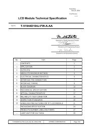
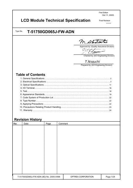
<strong>LCD</strong> Module Technical Specification<br />
T-<strong>51750GD065J</strong>-<strong>FW</strong>-<strong>ADN</strong><br />
Table of Contents<br />
1. General Specifications .................................................................................................................................. 2<br />
2. Electrical Specifications ............................................................................................................................... 3<br />
3. Optical Specifications ................................................................................................................................. 11<br />
4. I/O Terminal.................................................................................................................................................... 16<br />
5. Test................................................................................................................................................................... 18<br />
6. Appearance Standards................................................................................................................................ 19<br />
7. Code System of Production Lot............................................................................................................... 22<br />
8. Type Number.................................................................................................................................................. 22<br />
9. Applying Precautions .................................................................................................................................. 22<br />
10. Precautions Relating Product Handling................................................................................................ 23<br />
11. Warranty ........................................................................................................................................................ 24<br />
Revision History<br />
Rev. Date Page Comment<br />
First Edition<br />
Oct 11, 2005<br />
Final Revision<br />
******<br />
Checked by (ACI Engineering Division)<br />
T-<strong>51750GD065J</strong>-<strong>FW</strong>-<strong>ADN</strong> (AD) No. 2005-0498 OPTREX CORPORATION Page 1/24<br />
)<br />
Approved by (Quality Assurance Division)<br />
)<br />
T.Noguchi<br />
Prepared by (ACI Engineering Division)
1. General Specifications<br />
Operating Temperature : min. -25 deg. to max. 75 deg.(*Note)<br />
Storage Temperature : min. -25 deg. to max. 85 deg.<br />
Resolution : 640 x 3 [R.G.B] (W) x 480 (H) dots<br />
Dot pitch : 0.069 x 3 [R.G.B] (W) x 0.207 (V) mm<br />
Pixel arrangement : RGB-Stripe<br />
Color depth : 262,144 colors<br />
Active Viewing Area : 132.5 (W) x 99.4 (H) mm<br />
Outline dimensions * : 158.0 (W) x 120.36 (H) x 10.75 (D) mm<br />
Weight : 190 g typ.<br />
* Excluding backlight cables.<br />
<strong>LCD</strong> type : Normally white-mode / Transmissive<br />
Viewing angle : 6:00<br />
Interface : 18-bit parallel data transfer (6-bit / color)<br />
Backlight * : CCFL, Edge lighting type 2-tubes, replaceable<br />
Surface Treatment : AG Coating<br />
* Backlight driving DC/AC inverter is not built in this module.<br />
Appendix : Method of replacing the lamp unit<br />
: UL LABEL<br />
Drawings : Dimensional Outline UE-313014<br />
Lead free : Our product corresponds to lead free.<br />
Lead free is defined as below:<br />
The solder used in the <strong>LCD</strong> module.<br />
Electrical components (Terminal section) used in the <strong>LCD</strong> module.<br />
Any lead used within the electrical component does not apply to<br />
our module definition of lead free.<br />
Note : Operation temperature range defines the operation only.<br />
Electrical and optical specification can be guaranteed at the condition that ambient<br />
temperature is 25°C.<br />
T-<strong>51750GD065J</strong>-<strong>FW</strong>-<strong>ADN</strong> (AD) No. 2005-0498 OPTREX CORPORATION Page 2/24
2. Electrical specifications<br />
2.1. Absolute Maximum Ratings<br />
Parameter Symbol Conditions Min. Max. Unit<br />
Supply Voltage for <strong>LCD</strong> VCC - 0 5.5 V<br />
Logic Input Voltage VI - 0 7.0 V<br />
2.2. DC characteristics<br />
(1) <strong>TFT</strong>-<strong>LCD</strong> Ambient Temperature : Ta = 25°C<br />
ITEM SYMBOL MIN. TYP. MAX. UNIT Remarks<br />
Power Supply Voltages for <strong>LCD</strong><br />
Note A)<br />
Power Supply Currents for <strong>LCD</strong><br />
Note B)<br />
VCC<br />
ICC<br />
Permissive input ripple Voltage VRP<br />
Logic Input Voltage<br />
3.0 3.3 3.6 V for 3.3V system<br />
4.5 5.0 5.5 V for 5V system<br />
-- 240 -- mA for 3.3V system<br />
-- 180 -- mA for 5V system<br />
-- -- 100 mVp-p VCC=+3.3V<br />
-- -- 100 mVp-p VCC=+5.0V<br />
High VIH 2.4 -- 5.5 V VCC=MAX<br />
Low VIL 0 -- 0.8 V VCC=MIN<br />
T-<strong>51750GD065J</strong>-<strong>FW</strong>-<strong>ADN</strong> (AD) No. 2005-0498 OPTREX CORPORATION Page 3/24
[Note]<br />
A) Power and signals sequence:<br />
t1 ≤ 10 ms 200 ms < t6<br />
3.0V or 4.5V<br />
0.3V<br />
0 < t2 ≤ 50 ms 0 ≤ t7<br />
0 < t3 ≤ 50 ms<br />
0 < t4 ≤ 50 ms<br />
500 ms < t5<br />
VCC-dip conditions:<br />
1) When 2.4 V ≤ VCC < 3.0 V, td ≤ 10 ms<br />
2) When VCC < 2.4 V<br />
VCC-dip conditions should also follow the power and signals sequence.<br />
B) Typical current condition:<br />
64- gray- bar-pattern<br />
480 line mode<br />
VCC = +3.3 V, f H=31.5kHz, f V=60Hz, f CLK= 25MHz<br />
VCC = +5.0 V, f H=31.5kHz, f V=60Hz, f CLK= 25MHz<br />
C) For typical luminance of 400 cd/m 2<br />
VCC<br />
data<br />
t1 t2 t3<br />
Backlight<br />
3.0V or 4.5V<br />
t4 t5<br />
t6 t7<br />
data: RGB DATA, DCLK, HD, VD, DENA<br />
td<br />
0.3V 0.3V<br />
T-<strong>51750GD065J</strong>-<strong>FW</strong>-<strong>ADN</strong> (AD) No. 2005-0498 OPTREX CORPORATION Page 4/24<br />
2.4 V<br />
3.0 V or 4.5V<br />
VCC
2.5. Pixel Alignment<br />
B R G B R G B R G B R G B<br />
G B R G B R G B R G B R G B R<br />
G B R G B R G B R G B R G B R<br />
G B R G B R G B R G B R G B<br />
G B R G B<br />
T-<strong>51750GD065J</strong>-<strong>FW</strong>-<strong>ADN</strong> (AD) No. 2005-0498 OPTREX CORPORATION Page 7/24<br />
G B<br />
G B R G B R G B R G B R G B<br />
B R G B R G B<br />
R G B R G B R G<br />
R G B<br />
R G B<br />
R G<br />
R
2.6. Color Data Assignment<br />
R DATA G DATA B DATA<br />
COLOR INPUT MSB LSB MSB LSB MSB LSB<br />
DATA R5 R4 R3 R2 R1 R0 G5 G4 G3 G2 G1 G0 B5 B4 B3 B2 B1 B0<br />
BLACK 0 0 0 0 0 0 0 0 0 0 0 0 0 0 0 0 0 0<br />
RED (63) 1 1 1 1 1 1 0 0 0 0 0 0 0 0 0 0 0 0<br />
GREEN (63) 0 0 0 0 0 0 1 1 1 1 1 1 0 0 0 0 0 0<br />
BASIC BLUE (63) 0 0 0 0 0 0 0 0 0 0 0 0 1 1 1 1 1 1<br />
COLOR CYAN 0 0 0 0 0 0 1 1 1 1 1 1 1 1 1 1 1 1<br />
RED<br />
GREEN<br />
[Note]<br />
BLUE<br />
MAGENTA 1 1 1 1 1 1 0 0 0 0 0 0 1 1 1 1 1 1<br />
YELLOW 1 1 1 1 1 1 1 1 1 1 1 1 0 0 0 0 0 0<br />
WHITE 1 1 1 1 1 1 1 1 1 1 1 1 1 1 1 1 1 1<br />
RED (0) 0 0 0 0 0 0 0 0 0 0 0 0 0 0 0 0 0 0<br />
RED (1) 0 0 0 0 0 1 0 0 0 0 0 0 0 0 0 0 0 0<br />
RED (2) 0 0 0 0 1 0 0 0 0 0 0 0 0 0 0 0 0 0<br />
RED (62) 1 1 1 1 1 0 0 0 0 0 0 0 0 0 0 0 0 0<br />
RED (63) 1 1 1 1 1 1 0 0 0 0 0 0 0 0 0 0 0 0<br />
GREEN (0) 0 0 0 0 0 0 0 0 0 0 0 0 0 0 0 0 0 0<br />
GREEN (1) 0 0 0 0 0 0 0 0 0 0 0 1 0 0 0 0 0 0<br />
GREEN (2) 0 0 0 0 0 0 0 0 0 0 1 0 0 0 0 0 0 0<br />
GREEN (62) 0 0 0 0 0 0 1 1 1 1 1 0 0 0 0 0 0 0<br />
GREEN (63) 0 0 0 0 0 0 1 1 1 1 1 1 0 0 0 0 0 0<br />
BLUE (0) 0 0 0 0 0 0 0 0 0 0 0 0 0 0 0 0 0 0<br />
BLUE (1) 0 0 0 0 0 0 0 0 0 0 0 0 0 0 0 0 0 1<br />
BLUE (2) 0 0 0 0 0 0 0 0 0 0 0 0 0 0 0 0 1 0<br />
BLUE (62) 0 0 0 0 0 0 0 0 0 0 0 0 1 1 1 1 1 0<br />
BLUE (63) 0 0 0 0 0 0 0 0 0 0 0 0 1 1 1 1 1 1<br />
1) Definition of gray scale<br />
Color (n) --- n indicates gray scale level.<br />
Higher n means brighter level.<br />
2) Data 1:High, 0: Low<br />
T-<strong>51750GD065J</strong>-<strong>FW</strong>-<strong>ADN</strong> (AD) No. 2005-0498 OPTREX CORPORATION Page 8/24
1.1. Lighting Specifications<br />
Ta=25°C<br />
Parameter Symbol Conditions Min. Typ. Max. Units Notes<br />
Lamp Voltage VL - - 320 - Vrms 1<br />
Lamp Current IL - - 6.0 7.0 mArms 2<br />
Starting Voltage VS - - - 520 Vrms 3<br />
Surface Luminance L IL=6mA - 4500 - cd/m 2<br />
Average Life TAL IL=6mA 50,000 - - hrs 5<br />
Note 1 :The voltage ( r.m.s. ) to maintain the electric discharge of the lamp. It is measured after<br />
lighting for 3 minutes .<br />
Note 2 :The current ( r.m.s. ) to flow through the lamp with the electric discharge. It is measured<br />
after lighting for 3 minutes.<br />
Note 3 :The voltage at starting the electric discharge when the voltage is increased gradually<br />
from 0V.<br />
Note 4 :Surface Luminance is specified by the average of 9 luminance values measured at each<br />
point shown above after 20 minutes power on with the all ON pattern adjusted to maximum<br />
contrast and the dimming control of 100%. ( maximum brightness )<br />
Note 5 : CFL Life is defined as time period that the actual luminance becomes 50% or lower of its<br />
initial value.<br />
The Average life time of CFL is defined as the time when half or more of the testing CFLs<br />
have become less bright than 50% of the initial brightness at continuous operation.<br />
I<br />
N<br />
V<br />
VS VL<br />
CFL Testing Circuit<br />
Recommended Inverter : S-12645 ( Produced by ELEVAM )<br />
C<br />
F<br />
L<br />
T-<strong>51750GD065J</strong>-<strong>FW</strong>-<strong>ADN</strong> (AD) No. 2005-0498 OPTREX CORPORATION Page 10/24<br />
Y=60<br />
IL Measurement Points<br />
P1<br />
P4<br />
P7<br />
Y=320<br />
P2<br />
P5<br />
P8<br />
Y=580<br />
P3<br />
P6<br />
P9<br />
X=60<br />
X=240<br />
X=420<br />
4
4. I/O Terminal<br />
4.1 Pin assignment<br />
CN 1(INTERFACE SIGNAL)<br />
Used connector: DF9B-31P-1V (Hirose)<br />
Corresponding connector: DF9B-31S-1V (Hirose)<br />
Pin No. Symbol Function<br />
1 GND<br />
2 DCLK Clock signal for sampling catch data signal<br />
3 HD Horizontal sync signal<br />
4 VD Vertical sync signal<br />
5 GND<br />
6 R0 Red data signal(LSB)<br />
7 R1 Red data signal<br />
8 R2 Red data signal<br />
9 R3 Red data signal<br />
10 R4 Red data signal<br />
11 R5 Red data signal(MSB)<br />
12 GND<br />
13 G0 Green data signal(LSB)<br />
14 G1 Green data signal<br />
15 G2 Green data signal<br />
16 G3 Green data signal<br />
17 G4 Green data signal<br />
18 G5 Green data signal(MSB)<br />
19 GND<br />
20 B0 Blue data signal(LSB)<br />
21 B1 Blue data signal<br />
22 B2 Blue data signal<br />
23 B3 Blue data signal<br />
24 B4 Blue data signal<br />
25 B5 Blue data signal(MSB)<br />
26 GND<br />
27 DENA Data enable signal(to settle the viewing area)<br />
28 VCC Power Supply (DC 3.3V or 5V)<br />
29 VCC Power Supply (DC 3.3V or 5V)<br />
30 TEST This pin should be open. Test signal output for only internal test use.<br />
31 REV Reverse scan control. L = Normal, H = Reverse<br />
*) The shielding case is connected with GND<br />
CN 2, CN 3 (BACKLIGHT)<br />
Backlight-side connector: BHR-02(8.0)VS-1N(JST)<br />
Inverter-side connector: SM02(8.0)B-BHS(JST)<br />
Pin No. Symbol Function<br />
1 CTH VBLH(High Voltage)<br />
3 CTL VBLL(Low Voltage)<br />
[Note] VBLH-VBLL = VL<br />
T-<strong>51750GD065J</strong>-<strong>FW</strong>-<strong>ADN</strong> (AD) No. 2005-0498 OPTREX CORPORATION Page 16/24
Timing signal<br />
Display data<br />
Power<br />
4.2. Block Diagram<br />
I/F Connector CN1<br />
Timing<br />
Converter<br />
Power<br />
Supply<br />
Circuit<br />
BACKLIGHT<br />
CCFL<br />
Driver(gate)<br />
CN2,CN3<br />
1<br />
3<br />
T-<strong>51750GD065J</strong>-<strong>FW</strong>-<strong>ADN</strong> (AD) No. 2005-0498 OPTREX CORPORATION Page 17/24<br />
G1<br />
G2<br />
G480<br />
S1<br />
BACKLIGHT CN2<br />
Driver(source)<br />
S2<br />
<strong>TFT</strong>-<strong>LCD</strong><br />
BACKLIGHT<br />
S1920<br />
CN3
5. Test<br />
No change on display and in operation under the following test condition.<br />
Conditions: Unless otherwise specified, tests will be conducted under the following condition.<br />
Temperature: 20±5°C<br />
Humidity : 65±5%RH<br />
tests will be not conducted under functioning state.<br />
No. Parameter Conditions Notes<br />
1 High Temperature Operating 60°C, 96hrs (operation state)<br />
2 High Temperature Storage 85°C, 96hrs 2<br />
3 Low Temperature Storage -25°C, 96hrs 1,2<br />
4 Damp Proof Test 40°C,90~95%RH, 96hrs 1,2<br />
5 Vibration Test Frequency:10-57Hz/Vibration width(one side):0.75mm 3<br />
:58-500Hz/Gravity:9.8m/s 2<br />
Sweep time:11minutes<br />
6 Shock Shock level:490m/s 2<br />
Test period:3hrs for each direction of X,Y,Z<br />
Waveform:half sinusoidal wave, 11ms<br />
Number of shocks :<br />
One shock input in each direction of three mutually<br />
perpendicular axis for a total of six shock inputs<br />
7 Shock Test To be measured after dropping from 60cm high on<br />
Note 1: No dew condensation to be observed.<br />
the concrete surface in packing state.<br />
Note 2: The function test shall be conducted after 4 hours storage at the normal<br />
Temperature and humidity after removed from the test chamber.<br />
Note 3: Vibration test will be conducted to the product itself without putting it in a container.<br />
E<br />
B<br />
T-<strong>51750GD065J</strong>-<strong>FW</strong>-<strong>ADN</strong> (AD) No. 2005-0498 OPTREX CORPORATION Page 18/24<br />
G D<br />
60cm<br />
A<br />
F<br />
C<br />
Concrete Surface<br />
Dropping method corner dropping<br />
A corner : once<br />
Edge dropping<br />
B,C,D edge : once<br />
Face dropping<br />
E,F,G face : once
6. Appearance Standards<br />
6.1.Inspection conditions<br />
The <strong>LCD</strong> shall be inspected under 40W white fluorescent light.<br />
The distance between the eyes and the sample shall be more than 30cm.<br />
All directions for inspecting the sample should be within 45°against perpendicular line.<br />
6.2.Definition of applicable Zones<br />
X<br />
X<br />
X<br />
X : Maximum Seal Line<br />
A Zone : Active display area<br />
B Zone : Out of active display area up to viewing area<br />
C Zone : Rest parts<br />
A Zone + B Zone = Viewing area<br />
T-<strong>51750GD065J</strong>-<strong>FW</strong>-<strong>ADN</strong> (AD) No. 2005-0498 OPTREX CORPORATION Page 19/24<br />
45°<br />
A Zone<br />
B Zone<br />
C Zone<br />
X
6.3 Standards<br />
No. Parameter Criteria<br />
1<br />
2<br />
3<br />
4<br />
Polarizer Scratches<br />
DENT<br />
BLACK and WHITE<br />
Zone Acceptable Number<br />
X(mm) Y(mm) A B C<br />
L ≤ 15 0.01 15 W > 0.01 0 *<br />
- W > 0.05 0 *<br />
X : Length, Y : Width * : Disregard<br />
Zone Acceptable Number<br />
Dimension (mm) A B C<br />
0.30 < D ≤ 0.50 4 *<br />
0.50 < D 0 *<br />
D : Average Diameter = (long+short)/2 * : Disregard<br />
SPOT BUBBLE Zone Acceptable Number<br />
LINT<br />
Dimension (mm) A B C<br />
0.30 < D ≤ 0.50 5 *<br />
0.50 < D 0 *<br />
Zone Acceptable Number<br />
X(mm) Y(mm) A B C<br />
L ≤ 3.0 W ≤ 0.15 4 *<br />
L > 3.0 W ≤ 0.15 0 *<br />
- W > 0.15 According to BLACK SPOT *<br />
X : Length, Y : Width * : Disregard<br />
T-<strong>51750GD065J</strong>-<strong>FW</strong>-<strong>ADN</strong> (AD) No. 2005-0498 OPTREX CORPORATION Page 20/24
No. Parameter Criteria<br />
5<br />
6<br />
(a) Bright Dot<br />
(b) Dark Dot Zone Acceptable Number<br />
TWO Adjacent Dot<br />
7 Three or More<br />
8<br />
Adjacent Dot<br />
Dimension (mm) A B C<br />
Bright Dot 7 (G ≤ 3) *<br />
Dark Dot 7 *<br />
TOTAL 10<br />
Zone Acceptable Number<br />
Dimension (mm) A B C<br />
Bright Dot 3 PAIRS *<br />
Dark Dot 3 PAIRS *<br />
NOT ALLOWED<br />
Zone Acceptable Number<br />
Dimension (mm) A B C<br />
Bright Dot 5 mm *<br />
Dark Dot 5 mm *<br />
9 Line Defect NOT ALLOWED<br />
Note 1: Bright Dot is defined as follows:<br />
Visible through 5% transmission ND filter under the condition that black image (color 0) is on the<br />
display.<br />
Note 2: Dark Dot is defined as follows:<br />
Recognizable darker than around under the condition that each R(63), G(63), B(63) image is on<br />
the display.<br />
Note 3: Definition of adjacent<br />
The defects that are not defined above and considered to be problem shall be reviewed and discussed by<br />
both parties.<br />
R G B R G B R G B<br />
R G B R G B R G B<br />
R G B R G B R G B<br />
Defective Dot<br />
Adjacent Dots<br />
T-<strong>51750GD065J</strong>-<strong>FW</strong>-<strong>ADN</strong> (AD) No. 2005-0498 OPTREX CORPORATION Page 21/24
7. Code System of Production Lot<br />
The production lot of module is specified as follows.<br />
8. Type Number<br />
Factory Number (0~9)<br />
Factory Code (Alphabet)<br />
Production Week (1~5)<br />
Production Month (1~9, X, Y, Z)<br />
Production Year (Lower 2 digits)<br />
The type number of module is specified as follows.<br />
T-<strong>51750GD065J</strong>-<strong>FW</strong>-<strong>ADN</strong><br />
9. Applying Precautions<br />
Factory Control Number (0~9)<br />
Date of the week (A~G)<br />
Please contact us when questions and/or new problems not specified in this<br />
Specifications arise.<br />
T-<strong>51750GD065J</strong>-<strong>FW</strong>-<strong>ADN</strong> (AD) No. 2005-0498 OPTREX CORPORATION Page 22/24
10. Precautions Relating Product Handling<br />
The Following precautions will guide you in handling our product correctly.<br />
1) Liquid crystal display devices<br />
1. The liquid crystal display device panel used in the liquid crystal display module is<br />
made of plate glass. Avoid any strong mechanical shock. Should the glass break<br />
handle it with care.<br />
2. The polarizer adhering to the surface of the <strong>LCD</strong> is made of a soft material.<br />
Guard against scratching it.<br />
2) Care of the liquid crystal display module against static electricity discharge.<br />
1. When working with the module, be sure to ground your body and any electrical<br />
equipment you may be using. We strongly recommend the use of anti static mats<br />
( made of rubber ), to protect work tables against the hazards of electrical shock.<br />
2. Avoid the use of work clothing made of synthetic fibers. We recommend cotton<br />
clothing or other conductivity-treated fibers.<br />
3. Slowly and carefully remove the protective film from the <strong>LCD</strong> module, since this<br />
operation can generate static electricity.<br />
3) When the <strong>LCD</strong> module alone must be stored for long periods of time:<br />
1. Protect the modules from high temperature and humidity.<br />
2. Keep the modules out of direct sunlight or direct exposure to ultraviolet rays.<br />
3. Protect the modules from excessive external forces.<br />
4) Use the module with a power supply that is equipped with an overcurrent protector<br />
circuit,since the module is not provided with this protective feature.<br />
5) Do not ingest the <strong>LCD</strong> fluid itself should it leak out of a damaged <strong>LCD</strong> module. Should<br />
hands or clothing come in contact with <strong>LCD</strong> fluid, wash immediately with soap.<br />
6) Conductivity is not guaranteed for models that use metal holders where solder<br />
connections between the metal holder and the PCB are not used. Please contact us<br />
to discuss appropriate ways to assure conductivity.<br />
7) For models which use CFL:<br />
1. High voltage of 1000V or greater is applied to the CFL cable connector area.<br />
Care should be taken not to touch connection areas to avoid burns.<br />
2. Protect CFL cables from rubbing against the unit and thus causing the wire jacket to<br />
become worn.<br />
3. The use of CFLs for extended periods of time at low temperatures will significantly<br />
shorten their service life.<br />
8) For models which use touch panels:<br />
1. Do not stack up modules since they can be damaged by components on neighboring modules.<br />
2. Do not place heavy objects on top of the product. This could cause glass breakage.<br />
9) For models which use COG,TAB,or COF:<br />
1. The mechanical strength of the product is low since the IC chip faces out unprotected<br />
from the rear. Be sure to protect the rear of the IC chip from external forces.<br />
2. Given the fact that the rear of the IC chip is left exposed, in order to protect the unit<br />
from electrical damage, avoid installation configurations in which the rear of the IC<br />
chip runs the risk of making any electrical contact.<br />
T-<strong>51750GD065J</strong>-<strong>FW</strong>-<strong>ADN</strong> (AD) No. 2005-0498 OPTREX CORPORATION Page 23/24
10) Models which use flexible cable, heat seal, or TAB:<br />
1. In order to maintain reliability, do not touch or hold by the connector area.<br />
2. Avoid any bending, pulling, or other excessive force, which can result in brokenconnections.<br />
11) have an adverse effect on connecting parts ( <strong>LCD</strong> panel-TCP / HEAT SEAL / FPC / etc.,<br />
PCB-TCP / HEAT SEAL / FPC etc., TCP-HEAT SEAL, TCP-FPC, HEAT SEAL-FPC,etc.,)<br />
depending on its materials.Please check and evaluate these materials carefully before use.<br />
12) In case of acrylic plate is attached to front side of <strong>LCD</strong> panel, cloudiness ( very small<br />
cracks ) can occur on acrylic plate, being influenced by some components generated<br />
from polarizer film. Please check and evaluate those acrylic materials carefully before use.<br />
11. Warranty<br />
This product has been manufactured to your company’s specifications as a part for use in<br />
your company’s general electronic products. It is guaranteed to perform according to<br />
delivery specifications. For any other use apart from general electronic equipment, we<br />
cannot take responsibility if the product is used in medical devices, nuclear power control<br />
equipment, aerospace equipment, fire and security systems, or any other applications in<br />
which there is a direct risk to human life and where extremely high levels of reliability are<br />
required. If the product is to be used in any of the above applications, we will need to enter<br />
into a separate product liability agreement.<br />
1. We cannot accept responsibility for any defect, which may arise from additional manufacturing of the<br />
product (including disassembly and reassembly), after product delivery.<br />
2. We cannot accept responsibility for any defect, which may arise after the application<br />
of strong external force to the product.<br />
3. We cannot accept responsibility for any defect, which may arise due to the application<br />
of static electricity after the product has passed your company’s acceptance inspection<br />
procedures.<br />
4. When the product is in CFL models, CFL service life and brightness will vary<br />
According to the performance of the inverter used, leaks, etc. We cannot accept<br />
responsibility for product performance, reliability, or defect, which may arise.<br />
5. We cannot accept responsibility for intellectual property of a third party, which may<br />
arise through the application of our product to your assembly with exception to those<br />
issues relating directly to the structure or method of manufacturing of our product.<br />
6. Optrex will not be held responsible for any quality guarantee issue for defect products<br />
judged as Optrex-origin longer than 2 (two) years from Optrex production or 1(one)<br />
year from Optrex, Optrex America, Optrex Europe delivery which ever comes later.<br />
T-<strong>51750GD065J</strong>-<strong>FW</strong>-<strong>ADN</strong> (AD) No. 2005-0498 OPTREX CORPORATION Page 24/24