Design Theory for High-Order Incremental Converters
Design Theory for High-Order Incremental Converters
Design Theory for High-Order Incremental Converters

Create successful ePaper yourself
Turn your PDF publications into a flip-book with our unique Google optimized e-Paper software.
Rearranging Eq. (4),2! 1−(n − 1)n c 1 b V ref
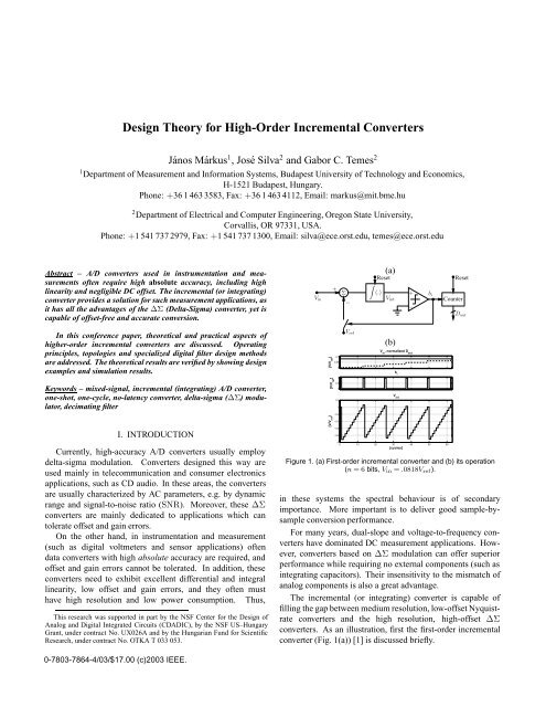
0 100 200 300 400 500 600 700 800 900 10002 x 10−3(a)0.5(a)1.5w 110.250.502 x 10−3(b)e q[LSB]0−0.25w 21.51−0.5−0.6 −0.4 −0.2 0 0.2 0.4 0.60.500 100 200 300 400 500 600 700 800 900 10003 x (c)10−310.5(b)w 32100 100 200 300 400 500 600 700 800 900 1000samplesV int2/V ref0−0.5Figure 4. Weighting functions of Cascade-of-Integrators (CoI) filters <strong>for</strong>1000 samples. (a) 1 integrator; (b) 2 integrators; (c) 3 integrators.However, in a higher-order structure, multiple integratorsare used <strong>for</strong> the calculation of the output. Since the converteroperates in transient mode, the digital filter can be implementedby an accumulate-and-dump structure. Hence, thefinal output of this filter is a weighted sum of the modulator’soutput samples. Fig. 4 shows the weighting functions of threedigital Cascade-of-Integrators (CoI) filters. Clearly, due to thenon-symmetrical weighting of higher-order filters, the periodicdisturbances cannot be eliminated.A first-order cancellation can be achieved, however, byincluding a sample-and-hold (S/H) stage at the input of theloop. If the system is operated at twice the noise frequency, andtwo consecutive outputs are averaged, a first-order cancellationcan still be achieved. In some applications, such as controlloops or multiplexed inputs, a S/H stage may be neededanyway.Simulation results (Fig. 5) show good agreement with thediscussions above. Fig. 5(a) shows the quantization errorof a second-order incremental converter, calculated from theoutput of the second digital integrator (with 10-bit resolution).Clearly, the resolution is only 10 bit due to the high error peaksat large inputs. Fig. 5(b) shows the inverted output of thesecond analog integrator at the end of the conversion. It canbe seen that Eq. (9) holds.B. Filtering Using Sinc L filtersIn DC and low-frequency measurements, it is importantto suppress environmental noises, especially line frequencydisturbances. In this section, another filtering technique isdiscussed, which is able to provide adequate suppression ofthese noises. The proposed method can be used <strong>for</strong> first- aswell as higher-order converters.The so-called sinc L filter [17], [18], optimized <strong>for</strong> ∆Σmodulators [16], [19], is the cascade of first-order averagingfilters, and thus it is capable of suppressing periodic distur-−1−0.6 −0.4 −0.2 0 0.2 0.4 0.6V in/V refFigure 5. Simulation result of a second-order system with 10 bitsresolution. (a) Quantization error; (b) Output of the second integrator(inverted).bances. Its transfer function isH (z)= 1M L (1+z −1 + ...+ z −M+1) L=( )1 1 − z−M LM L 1 − z −1 , (12)where L is the order of the filter, M is the decimation ratio,z = e sT , and T =1/f s . The free parameters of the filterare M and L. One can quickly conclude that the higher Mand L are, the better the resolution and the noise suppression.However, there are some conditions which must be satisfied bythese parameters.First, if the filter is used to suppress periodic noises atthe line frequency (f l ) and its multiples, then its first notch(f 1 = f s /M ) must be set to f l . This leaves f s as a variable todetermine. However, too large f s causes too tight requirements<strong>for</strong> the op-amps in the analog loop, while too small f scauses worse thermal noise (kT/C noise) suppression of theswitched-capacitor modulator.From the derivation of Sec. II it can be seen that the orderof the digital filter (L) must be at least the same as the orderof the analog loop (L a ). Analysis of classical ∆Σ structures[19] shows that much better per<strong>for</strong>mance can be achieved ifthe order of the digital filter L is greater by one than L a , i.e.L = L a +1. <strong>High</strong>er-order filters will not improve the SNR anyfurther.Another condition on L and M is that due to the transientoperation of this converter, all the registers of the digital filtermust be filled with valid data to get a correct digital output. Thetransient length of the filter (calculated from Eq. (12)) is N =LM − (L − 1). If it is realized as Cascaded Integrators andComb-filter stages [17], its length is somewhat greater: N =LM. This is the minimum number of cycles the filter has to beoperated <strong>for</strong> valid results.In Sec. II, the minimum number of clock periods (n) wasderived as a function of the required resolution (Eq. (10)).
However, the results were based on the Cascade-of-Integrators(CoI) filter structure (cf. the previous subsection). As the sinc Lfilter discussed here is not the optimal one, it needs more clockperiods <strong>for</strong> a required resolution.To fulfill all the above requirements, the following “cookbook”procedure is suggested:1. Choose the analog modulator order (L a =2, 3,...);2. This determines the order of the sinc filter (L = L a +1);3. Find n min = n, the required number of cycles usingEq. (10) and the iterative procedure described there;increase n min until L becomes its divider;4. Let M = n min /L;5. Simulate the whole system and check the achievableresolution;6. If the required n bit resolution is not achieved, increasen min with L;7. Repeat the last two steps until the desired resolution isachieved.8. When n min and thus M is found, the clock frequency canbe calculated as f s = Mf l , where f l is the line frequency.Note that with the increase of n min , the scaling coefficientsalso have to be updated to prevent the overflow of the analogintegrators. However, in practice, the algorithm is not toosensitive, and with a few iteration steps one can get goodparameters <strong>for</strong> a given resolution.Also, it should be noted that the described algorithm didnot take into account the presence of thermal noise, whichdepends on the sampling frequency and the capacitor valuesof the modulator. If the size of the capacitors becomes toolarge with the f s derived from the noiseless case above, thenf s must be increased until the desired SNR is achieved. In thiscase, the resolution limiting factor will be not the quantizationerror but the thermal noise.As an example <strong>for</strong> the ideal model, n min = 537 is required<strong>for</strong> a second-order modulator with u max =0.66V ref and 16-bitresolution. Using only second-order sinc-filter, the requirednumber of cycles <strong>for</strong> the same resolution becomes 1092,showing the ineffectiveness of this structure. However, usingthird-order sinc-filter, the required number of cycles drops ton = 576, which is hardly larger then the ideal one, whileat the same time it has the useful property of periodic noisesuppression.C. Improved Line Frequency SuppressionAs discussed in the previous section, incremental converterswith sinc-filters can suppress periodic noise disturbances, suchas the one coming from the power line. However, in somecritical applications the suppression available with simple sincfiltersmay not be adequate, especially if the line frequencyand/or the on-chip oscillator frequency can drift. In suchcases, the zeros of the digital filter can be staggered around thenotches, thus widening the frequency range around f l , wherethe rejection is high.attenuation of the filter [dB]−60−80−100−110−120−140−160−10 −8 −6 −4 −2 0 2 4 6 8 10deviation from the notch frequency [%]Figure 6. Transfer function of different filters around the line frequency:third-order sinc-filter (dash-dot line), fourth-order sinc-filter (dashedline) and fourth-order filter with staggered zeros (solid line).To modify the zeros of the filter, the rotated sinc filter (RS)[20] proposed <strong>for</strong> ∆Σ structures can be used. A second-orderfactor of its transfer function is of the <strong>for</strong>mH dec (z) = 1 − 2(cos Mα)z−M + z −2M1 − 2(cos α)z −1 + z −2 , (13)where z = e j2πf/fs and α represents the angle of the modifiedcomplex conjugate zeros. If α =0, the expression simplifiesto the transfer function of a second-order classical sinc filter.For the properties of this filter and the implementationdetails the reader is referred to [20] and [21]. Here, onlya comparison of different filtering and available rejections isdiscussed.Fig. 6 compares the achievable rejection around the linefrequency using various filter configurations. The dash-dot lineshows the rejection of a third-order sinc-filter around the linefrequency. The dashed line shows the rejection of a fourthordersinc-filter. Finally, the solid line illustrates the rejectionof the same fourth-order filter with modified zeros, and thuswith widened stopband. If the required attenuation of the linefrequency is −110 dB, then the third-order, fourth-order andmodified fourth-order filter can obtain this attenuation in theranges f l ± 1.5%, f l ± 4% and f l ± 6.5%, respectively.Similar techniques can be used to suppress both f l1 =50Hz and f l2 =60Hz simultaneously, using the same clockfrequency.IV. COMPARISONTable I compares several different modulators using variousfilters. The resolution is 16 bits, while the total number ofcycles changes according to the discussions of the previoussections.The fastest settling time is obtained when the converters areused with same-order CoI filter. However, if the suppressionof the line frequency is also a requirement, then an Lth-ordermodulator with an L +1st-order sinc-filter may be the right