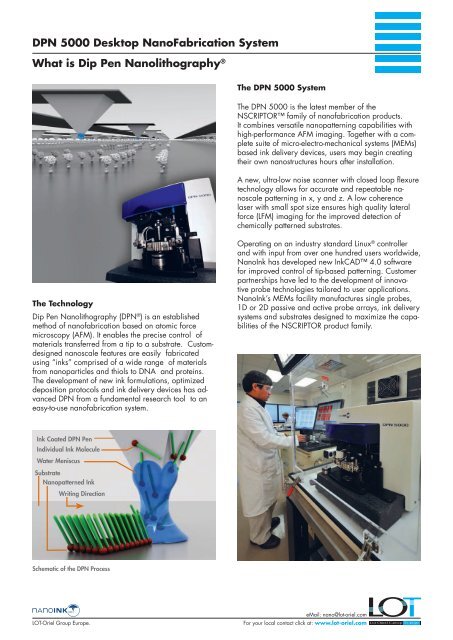
DPN 5000 Desktop NanoFabrication System What is Dip Pen ... - LAO
DPN 5000 Desktop NanoFabrication System What is Dip Pen ... - LAO
DPN 5000 Desktop NanoFabrication System What is Dip Pen ... - LAO

You also want an ePaper? Increase the reach of your titles
YUMPU automatically turns print PDFs into web optimized ePapers that Google loves.
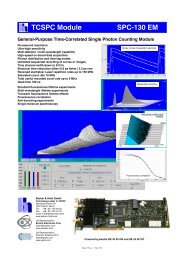
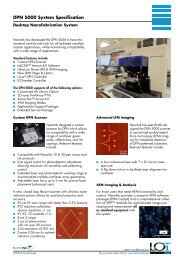
<strong>DPN</strong> <strong>5000</strong> <strong>Desktop</strong> <strong>NanoFabrication</strong> <strong>System</strong><strong>What</strong> <strong>is</strong> <strong>Dip</strong> <strong>Pen</strong> Nanolithography ®The <strong>DPN</strong> <strong>5000</strong> <strong>System</strong>The <strong>DPN</strong> <strong>5000</strong> <strong>is</strong> the latest member of theNSCRIPTOR family of nanofabrication products.It combines versatile nanopatterning capabilities withhigh-performance AFM imaging. Together with a completesuite of micro-electro-mechanical systems (MEMs)based ink delivery devices, users may begin creatingtheir own nanostructures hours after installation.A new, ultra-low no<strong>is</strong>e scanner with closed loop flexuretechnology allows for accurate and repeatable nanoscalepatterning in x, y and z. A low coherencelaser with small spot size ensures high quality lateralforce (LFM) imaging for the improved detection ofchemically patterned substrates.The Technology<strong>Dip</strong> <strong>Pen</strong> Nanolithography (<strong>DPN</strong> ® ) <strong>is</strong> an establ<strong>is</strong>hedmethod of nanofabrication based on atomic forcemicroscopy (AFM). It enables the prec<strong>is</strong>e control ofmaterials transferred from a tip to a substrate. Customdesignednanoscale features are easily fabricatedusing “inks” compr<strong>is</strong>ed of a wide range of materialsfrom nanoparticles and thiols to DNA and proteins.The development of new ink formulations, optimizeddeposition protocols and ink delivery devices has advanced<strong>DPN</strong> from a fundamental research tool to aneasy-to-use nanofabrication system.Operating on an industry standard Linux ® controllerand with input from over one hundred users worldwide,NanoInk has developed new InkCAD 4.0 softwarefor improved control of tip-based patterning. Customerpartnerships have led to the development of innovativeprobe technologies tailored to user applications.NanoInk’s MEMs facility manufactures single probes,1D or 2D passive and active probe arrays, ink deliverysystems and substrates designed to maximize the capabilitiesof the NSCRIPTOR product family.Ink Coated <strong>DPN</strong> <strong>Pen</strong>Individual Ink MoleculeWater Men<strong>is</strong>cusSubstrateNanopatterned InkWriting DirectionSchematic of the <strong>DPN</strong> ProcessLOT-Oriel Group Europe.eMail: nano@lot-oriel.comFor your local contact click at: www.lot-oriel.com
<strong>DPN</strong> <strong>5000</strong> <strong>Desktop</strong> <strong>NanoFabrication</strong> <strong>System</strong>Selected <strong>DPN</strong> ® ApplicationsNanoAffinity TemplatesUse <strong>DPN</strong> to pattern nanoscale features that direct thebinding and orientation of other nanoscale objects.Solid-State NanoPatterningDirectly deposit etch res<strong>is</strong>ts to create nanoscale patternsof any material on any substrate.Positive EtchNegative EtchSource:Wang, Y, et al,PNAS (2006) 103, 7.1 µm1 2 3<strong>DPN</strong> Templated Surface1. Charge Attraction2. Encoded Hybridization3. Specific Ligand BindingMHA nanoaffinity template controlling carbon nanotubes.6.0 4.04.02.02.0 0.0Y[µm] 0.0Y[µm] -2.0-2.0 -4.0-4.0 -6.0Z[nm]Z[nm]-6.00.0 50.0 -8.050.0-4.0-2.00.0 2.0 4.0 6.0 8.0-6.0 -4.0 -2.0 0.0 2.0 4.0 6.0X[µm]X[µm]Both positive and negative features are possible using<strong>DPN</strong> delivered etch res<strong>is</strong>ts. MHA nanoaffinity templatecontrolling carbon nanotubes.BioNanoUse <strong>DPN</strong> to create custom arrays of biomolecules.20 µm4 µm25 µm7 µmSource:Demers, LM, et al,Science (2002) 296.Source:Lee, KB, et al, Science(2002) 295, 5560.Source:Lenhert, S, et al, Small(2008) 4, 10.Image courtesy ofDr. Milan Mrksich Group,University of Chicago.Create true nanoscaleDNA arrays using <strong>DPN</strong>.Lysozyme nanoarraymade using <strong>DPN</strong>.Directly write modelphospholipid membranesto a surface.Use <strong>DPN</strong> to directly depositfibronectin arraysfor cell adhesion studies.Directed PlacementDecorate ex<strong>is</strong>ting micro/nano structures using <strong>DPN</strong>Image courtesy ofD3 Technologies Ltd,Glasgow UK.2 µm 2 µmKlarite ® : a commerciallyavailable surface enhancedRaman substrate.Use the <strong>DPN</strong> <strong>5000</strong> to inspect, image, map andselectively deposit in microwells.For more applications v<strong>is</strong>itwww.nanoink.netLOT-Oriel Group Europe.eMail: nano@lot-oriel.comFor your local contact click at: www.lot-oriel.com
<strong>DPN</strong> <strong>5000</strong> <strong>Desktop</strong> <strong>NanoFabrication</strong> <strong>System</strong>The Next Generation <strong>DPN</strong> ® <strong>System</strong>The Complete <strong>Desktop</strong> <strong>NanoFabrication</strong> <strong>System</strong>The <strong>DPN</strong> <strong>5000</strong> includes everything you need for tip-based nanofabrication.1 Complete AFM Imagingfor Nanoscale Pattern Analys<strong>is</strong>.2 InkCAD (Computer Aided Design) for <strong>DPN</strong> PatternsNext generation of advanced lithography control andanalys<strong>is</strong>.3 Custom <strong>DPN</strong> ScannerClosed loop 90 µm x, y, z flexure scanner for accurate and repeatablepatterning. Low coherence laser for improved imaging.214 Multiple Sample Stagesfor substrate handling, ink delivery and advancedenvironmental control of temperature and humidity.5 Custom MEMs for <strong>DPN</strong>Passive and active probe arrays, custom designed cantilevers,inkwells and substrates complement a variety of inks.435The Importance of MEMs for <strong>DPN</strong> ®Quality and cons<strong>is</strong>tency of <strong>DPN</strong> tips are the most importantvariables in determining the accuracy and reproducibilityof the resulting <strong>DPN</strong> patterns. NanoInk manufacturescustomized pens at its MEMs fabrication facility.Th<strong>is</strong> allows the monitoring and control of pen quality aswell as optimization for specific applications. Our siliconnitride pens differ from standard AFM probes with springconstants designed for writing with specific molecules.10,56 nmGuaranteed tip radii (10 – 15 nm) through SEM validation.Features of the <strong>DPN</strong> <strong>5000</strong>Nanoscale Prec<strong>is</strong>ionA closed-loop scannerwith superior linearityensures that nanoscaleprec<strong>is</strong>ion and accuracyare maintained.Controlled Feature SizeUse InkCal to executeand measure calibrationpattern, then use calculatedink diffusion rates tocontrol feature sizes.3 µm 3 µmOpen-loopClosed-loop1 µmLithography Resultant LFMCalibration Pattern ImageNanoInk <strong>is</strong> leading the development and application ofactive and passive multi-pen arrays to improve speedof deposition and enable large area patterning.Multiple Layer AlignmentUsing the <strong>DPN</strong> <strong>5000</strong>alignment wizards, writemultiple layers, with multipleinks, using multiplepens.Multi inks (ODTand MHA) coat amulti probe arrayODT5 µm MHALFM aftersecondaryODT deposition1D PassiveProbe ArrayActive <strong>Pen</strong> TM Array2D NanoPrintArray TMFully compatible ink delivery systems (Inkwells) havecon trolled surface reactivity. The hydrophobic and hydrophilicnature of the wells and the surrounding areasensures no cross-contamination of inks.Full Tip ControlThe <strong>DPN</strong> <strong>5000</strong> provideseasy access and controlof all tip movementspreventing unwanteddeposition.1 µm1 µmLithography ResultantCalibration Pattern LFM Imagewith tip lift without tip liftLOT-Oriel Group Europe.eMail: nano@lot-oriel.comFor your local contact click at: www.lot-oriel.com