

DS18S20 High-Precision 1-Wire Digital Thermometer
DS18S20 High-Precision 1-Wire Digital Thermometer
DS18S20 High-Precision 1-Wire Digital Thermometer

Create successful ePaper yourself
Turn your PDF publications into a flip-book with our unique Google optimized e-Paper software.
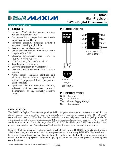
www.maxim-ic.comFEATURESUnique 1-<strong>Wire</strong> ® interface requires only oneport pin for communicationEach device has a unique 64-bit serial codestored in an onboard ROMMultidrop capability simplifies distributedtemperature sensing applicationsRequires no external componentsCan be powered from data line. Power supplyrange is 3.0V to 5.5VMeasures temperatures from –55°C to+125°C (–67°F to +257°F)0.5C accuracy from –10°C to +85°C9-bit thermometer resolutionConverts temperature in 750ms (max.)User-definable nonvolatile (NV) alarmsettingsAlarm search command identifies andaddresses devices whose temperature isoutside of programmed limits (temperaturealarm condition)Applications include thermostatic controls,industrial systems, consumer products,thermometers, or any thermally sensitivesystem<strong>DS18S20</strong><strong>High</strong>-<strong>Precision</strong>1-<strong>Wire</strong> <strong>Digital</strong> <strong>Thermometer</strong>PIN ASSIGNMENTDALLASDS18201GNDDQ12 3VDD2 3(BOTTOM VIEW)TO-92(<strong>DS18S20</strong>)NCNCV DDDQPIN DESCRIPTIONGND - GroundDQ - Data In/OutV DD - Power Supply VoltageNC - No Connect1234DS18208-Pin 150mil SO(<strong>DS18S20</strong>Z)8765NCNCNCGNDDESCRIPTIONThe <strong>DS18S20</strong> <strong>Digital</strong> <strong>Thermometer</strong> provides 9-bit centigrade temperature measurements and has analarm function with nonvolatile user-programmable upper and lower trigger points. The <strong>DS18S20</strong>communicates over a 1-<strong>Wire</strong> bus that by definition requires only one data line (and ground) forcommunication with a central microprocessor. It has an operating temperature range of –55°C to +125°Cand is accurate to 0.5C over the range of –10°C to +85°C. In addition, the <strong>DS18S20</strong> can derive powerdirectly from the data line (“parasite power”), eliminating the need for an external power supply.Each <strong>DS18S20</strong> has a unique 64-bit serial code, which allows multiple <strong>DS18S20</strong>s to function on the same1-<strong>Wire</strong> bus; thus, it is simple to use one microprocessor to control many <strong>DS18S20</strong>s distributed over alarge area. Applications that can benefit from this feature include HVAC environmental controls,temperature monitoring systems inside buildings, equipment or machinery, and process monitoring andcontrol systems.1-<strong>Wire</strong> is a registered trademark of Dallas Semiconductor.1 of 22 022103
ORDER INFORMATION<strong>DS18S20</strong>ORDERING PACKAGEDESCRIPTIONNUMBER MARKING<strong>DS18S20</strong> DS1820 <strong>DS18S20</strong> in 3-pin TO92<strong>DS18S20</strong>/T&R DS1820 <strong>DS18S20</strong> in 3-pin TO92, 2000 Piece Tape-and-Reel<strong>DS18S20</strong>+ DS1820 (See Note) <strong>DS18S20</strong> in Lead-Free 3-pin TO92<strong>DS18S20</strong>+T&R DS1820 (See Note) <strong>DS18S20</strong> in Lead-Free 3-pin TO92, 2000 Piece Tapeand-Reel<strong>DS18S20</strong>Z DS1820 <strong>DS18S20</strong> in 150 mil 8-pin SO<strong>DS18S20</strong>Z/T&R DS1820 <strong>DS18S20</strong> in 150 mil 8-pin SO, 2500 Piece Tape-and-Reel<strong>DS18S20</strong>Z+ DS1820 (See Note) <strong>DS18S20</strong> in Lead-Free 150 mil 8-pin SO<strong>DS18S20</strong>Z+T&R DS1820 (See Note) <strong>DS18S20</strong> in Lead-Free 150 mil 8-pin SO, 2500 PieceTape-and-ReelNote: A “+” symbol will also be marked on the package.DETAILED PIN DESCRIPTIONS Table 18-PIN SOIC* TO-92 SYMBOL DESCRIPTION5 1 GND Ground.4 2 DQ Data Input/Output Pin. Open-drain 1-<strong>Wire</strong> interface pin. Alsoprovides power to the device when used in parasite power mode(see “Parasite Power” section.)3 3 V DD Optional V DD Pin. V DD must be grounded for operation inparasite power mode.*All pins not specified in this table are “No Connect” pins.OVERVIEWFigure 1 shows a block diagram of the <strong>DS18S20</strong>, and pin descriptions are given in Table 1. The 64-bitROM stores the device’s unique serial code. The scratchpad memory contains the 2-byte temperatureregister that stores the digital output from the temperature sensor. In addition, the scratchpad providesaccess to the 1-byte upper and lower alarm trigger registers (T H and T L ). The T H and T L registers arenonvolatile (EEPROM), so they will retain data when the device is powered down.The <strong>DS18S20</strong> uses Dallas’ exclusive 1-<strong>Wire</strong> bus protocol that implements bus communication using onecontrol signal. The control line requires a weak pullup resistor since all devices are linked to the bus via a3-state or open-drain port (the DQ pin in the case of the <strong>DS18S20</strong>). In this bus system, the microprocessor(the master device) identifies and addresses devices on the bus using each device’s unique 64-bit code.Because each device has a unique code, the number of devices that can be addressed on one bus isvirtually unlimited. The 1-<strong>Wire</strong> bus protocol, including detailed explanations of the commands and “timeslots,” is covered in the 1-WIRE BUS SYSTEM section of this datasheet.Another feature of the <strong>DS18S20</strong> is the ability to operate without an external power supply. Power isinstead supplied through the 1-<strong>Wire</strong> pullup resistor via the DQ pin when the bus is high. The high bussignal also charges an internal capacitor (C PP ), which then supplies power to the device when the bus islow. This method of deriving power from the 1-<strong>Wire</strong> bus is referred to as “parasite power.” As analternative, the <strong>DS18S20</strong> may also be powered by an external supply on V DD .<strong>DS18S20</strong> BLOCK DIAGRAM Figure 1V PU4.7K PARASITE POWERCIRCUIT2 of 22MEMORY CONTROLLOGIC<strong>DS18S20</strong>
3 of 22<strong>DS18S20</strong>
<strong>DS18S20</strong>OPERATION — MEASURING TEMPERATUREThe core functionality of the <strong>DS18S20</strong> is its direct-to-digital temperature sensor. The temperature sensoroutput has 9-bit resolution, which corresponds to 0.5C steps. The <strong>DS18S20</strong> powers-up in a low-poweridle state; to initiate a temperature measurement and A-to-D conversion, the master must issue a ConvertT [44h] command. Following the conversion, the resulting thermal data is stored in the 2-bytetemperature register in the scratchpad memory and the <strong>DS18S20</strong> returns to its idle state. If the <strong>DS18S20</strong>is powered by an external supply, the master can issue “read-time slots” (see the 1-WIRE BUS SYSTEMsection) after the Convert T command and the <strong>DS18S20</strong> will respond by transmitting 0 while thetemperature conversion is in progress and 1 when the conversion is done. If the <strong>DS18S20</strong> is powered withparasite power, this notification technique cannot be used since the bus must be pulled high by a strongpullup during the entire temperature conversion. The bus requirements for parasite power are explained indetail in the POWERING THE <strong>DS18S20</strong> section of this datasheet.The <strong>DS18S20</strong> output data is calibrated in degrees centigrade; for Fahrenheit applications, a lookup tableor conversion routine must be used. The temperature data is stored as a 16-bit sign-extended two’scomplement number in the temperature register (see Figure 2). The sign bits (S) indicate if thetemperature is positive or negative: for positive numbers S = 0 and for negative numbers S = 1. Table 2gives examples of digital output data and the corresponding temperature reading.Resolutions greater than 9 bits can be calculated using the data from the temperature, COUNT REMAINand COUNT PER °C registers in the scratchpad. Note that the COUNT PER °C register is hard-wired to16 (10h). After reading the scratchpad, the TEMP_READ value is obtained by truncating the 0.5C bit(bit 0) from the temperature data (see Figure 2). The extended resolution temperature can then becalculated using the following equation:COUNT _ PER _ C COUNT _ REMAINTEMPERATURE TEMP _ READ 0.25 COUNT _ PER _ CTEMPERATURE REGISTER FORMAT Figure 2bit 7 bit 6 bit 5 bit 4 bit 3 bit 2 bit 1 bit 0LS Byte 2 6 2 5 2 4 2 3 2 2 2 1 2 0 2 -1bit 15 bit 14 bit 13 bit 12 bit 11 bit 10 bit 9 bit 8MS Byte S S S S S S S STEMPERATURE/DATA RELATIONSHIP Table 2TEMPERATUREDIGITAL OUTPUT(Binary)DIGITAL OUTPUT(Hex)+85.0°C* 0000 0000 1010 1010 00AAh+25.0°C 0000 0000 0011 0010 0032h+0.5°C 0000 0000 0000 0001 0001h0°C 0000 0000 0000 0000 0000h-0.5°C 1111 1111 1111 1111 FFFFh-25.0°C 1111 1111 1100 1110 FFCEh-55.0°C 1111 1111 1001 0010 FF92h*The power-on reset value of the temperature register is +85°C4 of 22
<strong>DS18S20</strong>OPERATION — ALARM SIGNALINGAfter the <strong>DS18S20</strong> performs a temperature conversion, the temperature value is compared to the userdefinedtwo’s complement alarm trigger values stored in the 1-byte T H and T L registers (see Figure 3).The sign bit (S) indicates if the value is positive or negative: for positive numbers S = 0 and for negativenumbers S = 1. The T H and T L registers are nonvolatile (EEPROM) so they will retain data when thedevice is powered down. T H and T L can be accessed through bytes 2 and 3 of the scratchpad as explainedin the MEMORY section of this datasheet.T H AND T L REGISTER FORMAT Figure 3bit 7 bit 6 bit 5 bit 4 bit 3 bit 2 bit 1 bit 0S 2 6 2 5 2 5 2 5 2 2 2 1 2 0Only bits 8 through 1 of the temperature register are used in the T H and T L comparison since T H and T Lare 8-bit registers. If the measured temperature is lower than or equal to T L or higher than T H , an alarmcondition exists and an alarm flag is set inside the <strong>DS18S20</strong>. This flag is updated after every temperaturemeasurement; therefore, if the alarm condition goes away, the flag will be turned off after the nexttemperature conversion.The master device can check the alarm flag status of all <strong>DS18S20</strong>s on the bus by issuing an Alarm Search[ECh] command. Any <strong>DS18S20</strong>s with a set alarm flag will respond to the command, so the master candetermine exactly which <strong>DS18S20</strong>s have experienced an alarm condition. If an alarm condition exists andthe T H or T L settings have changed, another temperature conversion should be done to validate the alarmcondition.POWERING THE <strong>DS18S20</strong>The <strong>DS18S20</strong> can be powered by an external supply on the V DD pin, or it can operate in “parasite power”mode, which allows the <strong>DS18S20</strong> to function without a local external supply. Parasite power is veryuseful for applications that require remote temperature sensing or that are very space constrained. Figure1 shows the <strong>DS18S20</strong>’s parasite-power control circuitry, which “steals” power from the 1-<strong>Wire</strong> bus viathe DQ pin when the bus is high. The stolen charge powers the <strong>DS18S20</strong> while the bus is high, and someof the charge is stored on the parasite power capacitor (C PP ) to provide power when the bus is low. Whenthe <strong>DS18S20</strong> is used in parasite power mode, the V DD pin must be connected to ground.In parasite power mode, the 1-<strong>Wire</strong> bus and C PP can provide sufficient current to the <strong>DS18S20</strong> for mostoperations as long as the specified timing and voltage requirements are met (refer to the DCELECTRICAL CHARACTERISTICS and the AC ELECTRICAL CHARACTERISTICS sections of this datasheet). However, when the <strong>DS18S20</strong> is performing temperature conversions or copying data from thescratchpad memory to EEPROM, the operating current can be as high as 1.5mA. This current can causean unacceptable voltage drop across the weak 1-<strong>Wire</strong> pullup resistor and is more current than can besupplied by C PP . To assure that the <strong>DS18S20</strong> has sufficient supply current, it is necessary to provide astrong pullup on the 1-<strong>Wire</strong> bus whenever temperature conversions are taking place or data is beingcopied from the scratchpad to EEPROM. This can be accomplished by using a MOSFET to pull the busdirectly to the rail as shown in Figure 4. The 1-<strong>Wire</strong> bus must be switched to the strong pullup within10s (max) after a Convert T [44h] or Copy Scratchpad [48h] command is issued, and the bus must beheld high by the pullup for the duration of the conversion (t conv ) or data transfer (t wr = 10ms). No otheractivity can take place on the 1-<strong>Wire</strong> bus while the pullup is enabled.The <strong>DS18S20</strong> can also be powered by the conventional method of connecting an external power supply tothe V DD pin, as shown in Figure 5. The advantage of this method is that the MOSFET pullup is notrequired, and the 1-<strong>Wire</strong> bus is free to carry other traffic during the temperature conversion time.5 of 22
<strong>DS18S20</strong>The use of parasite power is not recommended for temperatures above 100C since the <strong>DS18S20</strong> may notbe able to sustain communications due to the higher leakage currents that can exist at these temperatures.For applications in which such temperatures are likely, it is strongly recommended that the <strong>DS18S20</strong> bepowered by an external power supply.In some situations the bus master may not know whether the <strong>DS18S20</strong>s on the bus are parasite poweredor powered by external supplies. The master needs this information to determine if the strong bus pullupshould be used during temperature conversions. To get this information, the master can issue a Skip ROM[CCh] command followed by a Read Power Supply [B4h] command followed by a “read-time slot”.During the read-time slot, parasite powered <strong>DS18S20</strong>s will pull the bus low, and externally powered<strong>DS18S20</strong>s will let the bus remain high. If the bus is pulled low, the master knows that it must supply thestrong pullup on the 1-<strong>Wire</strong> bus during temperature conversions.SUPPLYING THE PARASITE-POWERED <strong>DS18S20</strong> DURING TEMPERATURECONVERSIONS Figure 4V PU<strong>DS18S20</strong>MicroprocessorV PU4.7k1-<strong>Wire</strong> BusGND DQV DDTo Other1-<strong>Wire</strong> DevicesPOWERING THE <strong>DS18S20</strong> WITH AN EXTERNAL SUPPLY Figure 5MicroprocessorV PU4.7k1-<strong>Wire</strong> Bus<strong>DS18S20</strong>GND DQV DDV DD (External Supply)To Other1-<strong>Wire</strong> Devices64-BIT LASERED ROM CODEEach <strong>DS18S20</strong> contains a unique 64-bit code (see Figure 6) stored in ROM. The least significant 8 bits ofthe ROM code contain the <strong>DS18S20</strong>’s 1-<strong>Wire</strong> family code: 10h. The next 48 bits contain a unique serialnumber. The most significant 8 bits contain a cyclic redundancy check (CRC) byte that is calculated fromthe first 56 bits of the ROM code. A detailed explanation of the CRC bits is provided in the CRCGENERATION section. The 64-bit ROM code and associated ROM function control logic allow the<strong>DS18S20</strong> to operate as a 1-<strong>Wire</strong> device using the protocol detailed in the 1-WIRE BUS SYSTEM sectionof this datasheet.64-BIT LASERED ROM CODE Figure 6MSB8-BIT CRC 48-BIT SERIAL NUMBER 8-BIT FAMILY CODE (10h)LSB MSBLSB MSBLSB6 of 22
<strong>DS18S20</strong>CRC GENERATIONCRC bytes are provided as part of the <strong>DS18S20</strong>’s 64-bit ROM code and in the 9 th byte of the scratchpadmemory. The ROM code CRC is calculated from the first 56 bits of the ROM code and is contained in themost significant byte of the ROM. The scratchpad CRC is calculated from the data stored in thescratchpad, and therefore it changes when the data in the scratchpad changes. The CRCs provide the busmaster with a method of data validation when data is read from the <strong>DS18S20</strong>. To verify that data hasbeen read correctly, the bus master must re-calculate the CRC from the received data and then comparethis value to either the ROM code CRC (for ROM reads) or to the scratchpad CRC (for scratchpad reads).If the calculated CRC matches the read CRC, the data has been received error free. The comparison ofCRC values and the decision to continue with an operation are determined entirely by the bus master.There is no circuitry inside the <strong>DS18S20</strong> that prevents a command sequence from proceeding if the<strong>DS18S20</strong> CRC (ROM or scratchpad) does not match the value generated by the bus master.The equivalent polynomial function of the CRC (ROM or scratchpad) is:CRC = X 8 + X 5 + X 4 + 1The bus master can re-calculate the CRC and compare it to the CRC values from the <strong>DS18S20</strong> using thepolynomial generator shown in Figure 8. This circuit consists of a shift register and XOR gates, and theshift register bits are initialized to 0. Starting with the least significant bit of the ROM code or the leastsignificant bit of byte 0 in the scratchpad, one bit at a time should shifted into the shift register. Aftershifting in the 56 th bit from the ROM or the most significant bit of byte 7 from the scratchpad, thepolynomial generator will contain the re-calculated CRC. Next, the 8-bit ROM code or scratchpad CRCfrom the <strong>DS18S20</strong> must be shifted into the circuit. At this point, if the re-calculated CRC was correct, theshift register will contain all 0s. Additional information about the Dallas 1-<strong>Wire</strong> cyclic redundancy checkis available in Application Note 27: Understanding and Using Cyclic Redundancy Checks with DallasSemiconductor Touch Memory Products.CRC GENERATOR Figure 8INPUTXOR XOR XOR(MSB)(LSB)8 of 22
<strong>DS18S20</strong>1-WIRE BUS SYSTEMThe 1-<strong>Wire</strong> bus system uses a single bus master to control one or more slave devices. The <strong>DS18S20</strong> isalways a slave. When there is only one slave on the bus, the system is referred to as a “single-drop”system; the system is “multidrop” if there are multiple slaves on the bus.All data and commands are transmitted least significant bit first over the 1-<strong>Wire</strong> bus.The following discussion of the 1-<strong>Wire</strong> bus system is broken down into three topics: hardwareconfiguration, transaction sequence, and 1-<strong>Wire</strong> signaling (signal types and timing).HARDWARE CONFIGURATIONThe 1-<strong>Wire</strong> bus has by definition only a single data line. Each device (master or slave) interfaces to thedata line via an open drain or 3-state port. This allows each device to “release” the data line when thedevice is not transmitting data so the bus is available for use by another device. The 1-<strong>Wire</strong> port of the<strong>DS18S20</strong> (the DQ pin) is open drain with an internal circuit equivalent to that shown in Figure 9.The 1-<strong>Wire</strong> bus requires an external pullup resistor of approximately 5k; thus, the idle state for the 1-<strong>Wire</strong> bus is high. If for any reason a transaction needs to be suspended, the bus MUST be left in the idlestate if the transaction is to resume. Infinite recovery time can occur between bits so long as the 1-<strong>Wire</strong>bus is in the inactive (high) state during the recovery period. If the bus is held low for more than 480s,all components on the bus will be reset.HARDWARE CONFIGURATION Figure 9V PU<strong>DS18S20</strong> 1-WIRE PORTR X4.7k1-wire BusDQPinR X5µATyp.T XT XR X = RECEIVET X = TRANSMIT100MOSFETTRANSACTION SEQUENCEThe transaction sequence for accessing the <strong>DS18S20</strong> is as follows:Step 1. InitializationStep 2. ROM Command (followed by any required data exchange)Step 3. <strong>DS18S20</strong> Function Command (followed by any required data exchange)It is very important to follow this sequence every time the <strong>DS18S20</strong> is accessed, as the <strong>DS18S20</strong> will notrespond if any steps in the sequence are missing or out of order. Exceptions to this rule are the SearchROM [F0h] and Alarm Search [ECh] commands. After issuing either of these ROM commands, themaster must return to Step 1 in the sequence.9 of 22
<strong>DS18S20</strong>INITIALIZATIONAll transactions on the 1-<strong>Wire</strong> bus begin with an initialization sequence. The initialization sequenceconsists of a reset pulse transmitted by the bus master followed by presence pulse(s) transmitted by theslave(s). The presence pulse lets the bus master know that slave devices (such as the <strong>DS18S20</strong>) are on thebus and are ready to operate. Timing for the reset and presence pulses is detailed in the1-WIRE SIGNALING section.ROM COMMANDSAfter the bus master has detected a presence pulse, it can issue a ROM command. These commandsoperate on the unique 64-bit ROM codes of each slave device and allow the master to single out a specificdevice if many are present on the 1-<strong>Wire</strong> bus. These commands also allow the master to determine howmany and what types of devices are present on the bus or if any device has experienced an alarmcondition. There are five ROM commands, and each command is 8 bits long. The master device mustissue an appropriate ROM command before issuing a <strong>DS18S20</strong> function command. A flowchart foroperation of the ROM commands is shown in Figure 14.SEARCH ROM [F0h]When a system is initially powered up, the master must identify the ROM codes of all slave devices onthe bus, which allows the master to determine the number of slaves and their device types. The masterlearns the ROM codes through a process of elimination that requires the master to perform a Search ROMcycle (i.e., Search ROM command followed by data exchange) as many times as necessary to identify allof the slave devices. If there is only one slave on the bus, the simpler Read ROM command (see below)can be used in place of the Search ROM process. For a detailed explanation of the Search ROMprocedure, refer to the iButton ® Book of Standards at www.ibutton.com/ibuttons/standard.pdf. Afterevery Search ROM cycle, the bus master must return to Step 1 (Initialization) in the transaction sequence.READ ROM [33h]This command can only be used when there is one slave on the bus. It allows the bus master to read theslave’s 64-bit ROM code without using the Search ROM procedure. If this command is used when thereis more than one slave present on the bus, a data collision will occur when all the slaves attempt torespond at the same time.MATCH ROM [55h]The match ROM command followed by a 64-bit ROM code sequence allows the bus master to address aspecific slave device on a multidrop or single-drop bus. Only the slave that exactly matches the 64-bitROM code sequence will respond to the function command issued by the master; all other slaves on thebus will wait for a reset pulse.SKIP ROM [CCh]The master can use this command to address all devices on the bus simultaneously without sending outany ROM code information. For example, the master can make all <strong>DS18S20</strong>s on the bus performsimultaneous temperature conversions by issuing a Skip ROM command followed by a Convert T [44h]command.Note that the Read Scratchpad [BEh] command can follow the Skip ROM command only if there is asingle slave device on the bus. In this case time is saved by allowing the master to read from the slavewithout sending the device’s 64-bit ROM code. A Skip ROM command followed by a Read Scratchpadcommand will cause a data collision on the bus if there is more than one slave since multiple devices willattempt to transmit data simultaneously.iButton is a registered trademark of Dallas Semiconductor.10 of 22
11 of 22<strong>DS18S20</strong>ALARM SEARCH [ECh]The operation of this command is identical to the operation of the Search ROM command except thatonly slaves with a set alarm flag will respond. This command allows the master device to determine ifany <strong>DS18S20</strong>s experienced an alarm condition during the most recent temperature conversion. Afterevery Alarm Search cycle (i.e., Alarm Search command followed by data exchange), the bus master mustreturn to Step 1 (Initialization) in the transaction sequence. Refer to the OPERATION — ALARMSIGNALING section for an explanation of alarm flag operation.<strong>DS18S20</strong> FUNCTION COMMANDSAfter the bus master has used a ROM command to address the <strong>DS18S20</strong> with which it wishes tocommunicate, the master can issue one of the <strong>DS18S20</strong> function commands. These commands allow themaster to write to and read from the <strong>DS18S20</strong>’s scratchpad memory, initiate temperature conversions anddetermine the power supply mode. The <strong>DS18S20</strong> function commands, which are described below, aresummarized in Table 4 and illustrated by the flowchart in Figure 15.CONVERT T [44h]This command initiates a single temperature conversion. Following the conversion, the resulting thermaldata is stored in the 2-byte temperature register in the scratchpad memory and the <strong>DS18S20</strong> returns to itslow-power idle state. If the device is being used in parasite power mode, within 10s (max) after thiscommand is issued the master must enable a strong pullup on the 1-<strong>Wire</strong> bus for the duration of theconversion (t conv ) as described in the POWERING THE <strong>DS18S20</strong> section. If the <strong>DS18S20</strong> is powered byan external supply, the master can issue read-time slots after the Convert T command and the <strong>DS18S20</strong>will respond by transmitting 0 while the temperature conversion is in progress and 1 when the conversionis done. In parasite power mode this notification technique cannot be used since the bus is pulled high bythe strong pullup during the conversion.WRITE SCRATCHPAD [4Eh]This command allows the master to write 2 bytes of data to the <strong>DS18S20</strong>’s scratchpad. The first byte iswritten into the T H register (byte 2 of the scratchpad), and the second byte is written into the T L register(byte 3 of the scratchpad). Data must be transmitted least significant bit first. Both bytes MUST bewritten before the master issues a reset, or the data may be corrupted.READ SCRATCHPAD [BEh]This command allows the master to read the contents of the scratchpad. The data transfer starts with theleast significant bit of byte 0 and continues through the scratchpad until the 9 th byte (byte 8 – CRC) isread. The master may issue a reset to terminate reading at any time if only part of the scratchpad data isneeded.COPY SCRATCHPAD [48h]This command copies the contents of the scratchpad T H and T L registers (bytes 2 and 3) to EEPROM. Ifthe device is being used in parasite power mode, within 10s (max) after this command is issued themaster must enable a strong pullup on the 1-<strong>Wire</strong> bus for at least 10ms as described in the POWERINGTHE <strong>DS18S20</strong> section.RECALL E 2 [B8h]This command recalls the alarm trigger values (T H and T L ) from EEPROM and places the data in bytes 2and 3, respectively, in the scratchpad memory. The master device can issue read-time slots following theRecall E 2 command and the <strong>DS18S20</strong> will indicate the status of the recall by transmitting 0 while therecall is in progress and 1 when the recall is done. The recall operation happens automatically at powerup,so valid data is available in the scratchpad as soon as power is applied to the device.
<strong>DS18S20</strong>READ POWER SUPPLY [B4h]The master device issues this command followed by a read-time slot to determine if any <strong>DS18S20</strong>s on thebus are using parasite power. During the read-time slot, parasite powered <strong>DS18S20</strong>s will pull the bus low,and externally powered <strong>DS18S20</strong>s will let the bus remain high. Refer to the POWERING THE <strong>DS18S20</strong>section for usage information for this command.<strong>DS18S20</strong> FUNCTION COMMAND SET Table 4Command Description Protocol1-<strong>Wire</strong> Bus ActivityAfter Command is Issued NotesTEMPERATURE CONVERSION COMMANDSConvert T Initiates temperature44h <strong>DS18S20</strong> transmits conversion 1conversion.status to master (not applicablefor parasite-powered <strong>DS18S20</strong>s).MEMORY COMMANDSRead Scratchpad Reads the entire scratchpad BEh <strong>DS18S20</strong> transmits up to 9 data 2including the CRC byte.bytes to master.Write Scratchpad Writes data into scratchpad 4Eh Master transmits 2 data bytes to 3bytes 2 and 3 (T H and T L ).<strong>DS18S20</strong>.Copy Scratchpad Copies T H and T L data from 48h None 1the scratchpad to EEPROM.Recall E 2 Recalls T H and T L data from B8h <strong>DS18S20</strong> transmits recall statusRead PowerSupplyEEPROM to the scratchpad.Signals <strong>DS18S20</strong> powersupply mode to the master.B4hto master.<strong>DS18S20</strong> transmits supply statusto master.NOTES:1) For parasite-powered <strong>DS18S20</strong>s, the master must enable a strong pullup on the 1-<strong>Wire</strong> bus duringtemperature conversions and copies from the scratchpad to EEPROM. No other bus activity may takeplace during this time.2) The master can interrupt the transmission of data at any time by issuing a reset.3) Both bytes must be written before a reset is issued.12 of 22
<strong>DS18S20</strong>1-WIRE SIGNALINGThe <strong>DS18S20</strong> uses a strict 1-<strong>Wire</strong> communication protocol to insure data integrity. Several signal typesare defined by this protocol: reset pulse, presence pulse, write 0, write 1, read 0, and read 1. All of thesesignals, with the exception of the presence pulse, are initiated by the bus master.INITIALIZATION PROCEDURE: RESET AND PRESENCE PULSESAll communication with the <strong>DS18S20</strong> begins with an initialization sequence that consists of a reset pulsefrom the master followed by a presence pulse from the <strong>DS18S20</strong>. This is illustrated in Figure 10. Whenthe <strong>DS18S20</strong> sends the presence pulse in response to the reset, it is indicating to the master that it is onthe bus and ready to operate.During the initialization sequence the bus master transmits (T X ) the reset pulse by pulling the 1-<strong>Wire</strong> buslow for a minimum of 480s. The bus master then releases the bus and goes into receive mode (R X ).When the bus is released, the 5k pullup resistor pulls the 1-<strong>Wire</strong> bus high. When the <strong>DS18S20</strong> detectsthis rising edge, it waits 15s to 60s and then transmits a presence pulse by pulling the 1-<strong>Wire</strong> bus lowfor 60s to 240s.INITIALIZATION TIMING Figure 10V PU1-WIRE BUSGNDMASTER T X RESET PULSE480s minimum<strong>DS18S20</strong>waits 15-60 sMASTER R X480s minimum<strong>DS18S20</strong> T Xpresence pulse60-240 sLINE TYPE LEGENDBus master pulling low<strong>DS18S20</strong> pulling lowResistor pullupREAD/WRITE TIME SLOTSThe bus master writes data to the <strong>DS18S20</strong> during write time slots and reads data from the <strong>DS18S20</strong>during read-time slots. One bit of data is transmitted over the 1-<strong>Wire</strong> bus per time slot.WRITE TIME SLOTSThere are two types of write time slots: “Write 1” time slots and “Write 0” time slots. The bus masteruses a Write 1 time slot to write a logic 1 to the <strong>DS18S20</strong> and a Write 0 time slot to write a logic 0 to the<strong>DS18S20</strong>. All write time slots must be a minimum of 60s in duration with a minimum of a 1s recoverytime between individual write slots. Both types of write time slots are initiated by the master pulling the1-<strong>Wire</strong> bus low (see Figure 11).To generate a Write 1 time slot, after pulling the 1-<strong>Wire</strong> bus low, the bus master must release the 1-<strong>Wire</strong>bus within 15s. When the bus is released, the 5k pullup resistor will pull the bus high. To generate aWrite 0 time slot, after pulling the 1-<strong>Wire</strong> bus low, the bus master must continue to hold the bus low forthe duration of the time slot (at least 60s). The <strong>DS18S20</strong> samples the 1-<strong>Wire</strong> bus during a window thatlasts from 15s to 60s after the master initiates the write time slot. If the bus is high during the samplingwindow, a 1 is written to the <strong>DS18S20</strong>. If the line is low, a 0 is written to the <strong>DS18S20</strong>.13 of 22
<strong>DS18S20</strong>READ-TIME SLOTSThe <strong>DS18S20</strong> can only transmit data to the master when the master issues read-time slots. Therefore, themaster must generate read-time slots immediately after issuing a Read Scratchpad [BEh] or Read PowerSupply [B4h] command, so that the <strong>DS18S20</strong> can provide the requested data. In addition, the master cangenerate read-time slots after issuing Convert T [44h] or Recall E 2 [B8h] commands to find out the statusof the operation as explained in the <strong>DS18S20</strong> FUNCTION COMMAND section.All read-time slots must be a minimum of 60s in duration with a minimum of a 1s recovery timebetween slots. A read-time slot is initiated by the master device pulling the 1-<strong>Wire</strong> bus low for aminimum of 1s and then releasing the bus (see Figure 11). After the master initiates the read-time slot,the <strong>DS18S20</strong> will begin transmitting a 1 or 0 on bus. The <strong>DS18S20</strong> transmits a 1 by leaving the bus highand transmits a 0 by pulling the bus low. When transmitting a 0, the <strong>DS18S20</strong> will release the bus by theend of the time slot, and the bus will be pulled back to its high idle state by the pullup resister. Outputdata from the <strong>DS18S20</strong> is valid for 15s after the falling edge that initiated the read-time slot. Therefore,the master must release the bus and then sample the bus state within 15s from the start of the slot.Figure 12 illustrates that the sum of T INIT , T RC , and T SAMPLE must be less than 15s for a read-time slot.Figure 13 shows that system timing margin is maximized by keeping T INIT and T RC as short as possibleand by locating the master sample time during read-time slots towards the end of the 15s period.READ/WRITE TIME SLOT TIMING DIAGRAM Figure 11STARTOF SLOTSTARTOF SLOTMASTER WRITE “0” SLOT60s < T X “0” < 120sMASTER WRITE “1” SLOT1s < T REC < > 1sV PU1-WIRE BUSGND<strong>DS18S20</strong> SamplesMIN TYP MAX<strong>DS18S20</strong> SamplesMIN TYP MAX15s 15s30s15s 15s 30sV PU1-WIRE BUSMASTER READ “0” SLOTMASTER READ “1” SLOT1s < T REC < GND> 1sMaster samples> 1 sMaster samples15s45s15sLINE TYPE LEGENDBus master pulling low<strong>DS18S20</strong> pulling lowResistor pullup14 of 22
DETAILED MASTER READ 1 TIMING Figure 12<strong>DS18S20</strong>V PU1-WIRE BUSVIH of MasterGNDT INT > 1sT RCMaster samples15sRECOMMENDED MASTER READ 1 TIMING Figure 13V PU1-WIRE BUSVIH of MasterGNDT INT =smallT RC =small15sMaster samplesLINE TYPE LEGENDBus master pulling lowResistor pullup15 of 22
ROM COMMANDS FLOW CHART Figure 14<strong>DS18S20</strong>InitializationSequenceMASTER TXRESET PULSE<strong>DS18S20</strong> TXPRESENCEPULSEMASTER TX ROMCOMMAND33hREAD ROMCOMMAND55hF0hCChNEChNN NMATCH ROMSEARCH ROMALARM SEARCHSKIP ROM NCOMMANDCOMMANDCOMMANDCOMMANDY Y Y Y YMASTER TXBIT 0<strong>DS18S20</strong> TX BIT 0<strong>DS18S20</strong> TX BIT 0<strong>DS18S20</strong> TX BIT 0<strong>DS18S20</strong> TX BIT 0MASTER TX BIT 0MASTER TX BIT 0<strong>DS18S20</strong> TXFAMILY CODE1 BYTEBIT 0MATCH?NNBIT 0MATCH?DEVICE(S)WITH ALARMFLAG SET?N<strong>DS18S20</strong> TXSERIAL NUMBER6 BYTESYYY<strong>DS18S20</strong> TX BIT 1<strong>DS18S20</strong> TXCRC BYTEMASTER TXBIT 1<strong>DS18S20</strong> TX BIT 1MASTER TX BIT 1BIT 1MATCH?NNBIT 1MATCH?YY<strong>DS18S20</strong> TX BIT 63MASTER TXBIT 63<strong>DS18S20</strong> TX BIT 63MASTER TX BIT 63BIT 63MATCH?NNBIT 63MATCH?YYMASTER TXFUNCTIONCOMMAND(FIGURE 15)16 of 22
<strong>DS18S20</strong> FUNCTION COMMANDS FLOW CHART Figure 15<strong>DS18S20</strong>MASTER TXFUNCTIONCOMMAND44hCONVERTTEMPERATURE?N48hCOPYSCRATCHPAD?NYYNPARASITEPOWER?YNPARASITEPOWER?Y<strong>DS18S20</strong> BEGINSCONVERSIONMASTER ENABLESSTRONG PULLUP ON DQMASTER ENABLESSTRONG PULL-UP ON DQDEVICECONVERTINGTEMPERATURE?YN<strong>DS18S20</strong> CONVERTSTEMPERATUREMASTER DISABLESSTRONG PULLUPCOPY INPROGRESS?YNDATA COPIED FROMSCRATCHPAD TO EEPROMMASTER DISABLESSTRONG PULLUPMASTERRX “0s”MASTERRX “1s”MASTERRX “0s”MASTERRX “1s”NB4hREADPOWER SUPPLY?NB8hRECALL E 2?NBEhREADSCRATCHPAD?N4EhWRITESCRATCHPAD?YYYYNPARASITEPOWERED?YMASTER BEGINS DATARECALL FROM E 2 PROMMASTER RX DATA BYTEFROM SCRATCHPADMASTER TX TH BYTETO SCRATCHPADMASTER TX TL BYTETO SCRATCHPADMASTERRX “1s”MASTERRX “0s”DEVICEBUSY RECALLINGDATA?NMASTERTX RESET?NYYNHAVE 8 BYTESBEEN READ?MASTERRX “0s”MASTERRX “1s”YMASTER RX SCRATCHPADCRC BYTERETURN TO INITIALIZATIONSEQUENCE (FIGURE 14) FORNEXT TRANSACTION17 of 22
<strong>DS18S20</strong> OPERATION EXAMPLE 1In this example there are multiple <strong>DS18S20</strong>s on the bus and they are using parasite power. The busmaster initiates a temperature conversion in a specific <strong>DS18S20</strong> and then reads its scratchpad andrecalculates the CRC to verify the data.<strong>DS18S20</strong>MASTER MODE DATA (LSB FIRST) COMMENTSTX Reset Master issues reset pulse.RX Presence <strong>DS18S20</strong>s respond with presence pulse.TX 55h Master issues Match ROM command.TX 64-bit ROM code Master sends <strong>DS18S20</strong> ROM code.TX 44h Master issues Convert T command.TXDQ line held high bystrong pullupMaster applies strong pullup to DQ for the duration of theconversion (t conv ).TX Reset Master issues reset pulse.RX Presence <strong>DS18S20</strong>s respond with presence pulse.TX 55h Master issues Match ROM command.TX 64-bit ROM code Master sends <strong>DS18S20</strong> ROM code.TX BEh Master issues Read Scratchpad command.RX 9 data bytes Master reads entire scratchpad including CRC. The masterthen recalculates the CRC of the first eight data bytes from thescratchpad and compares the calculated CRC with the readCRC (byte 9). If they match, the master continues; if not, theread operation is repeated.<strong>DS18S20</strong> OPERATION EXAMPLE 2In this example there is only one <strong>DS18S20</strong> on the bus and it is using parasite power. The master writes tothe T H and T L registers in the <strong>DS18S20</strong> scratchpad and then reads the scratchpad and recalculates theCRC to verify the data. The master then copies the scratchpad contents to EEPROM.MASTER MODE DATA (LSB FIRST) COMMENTSTX Reset Master issues reset pulse.RX Presence <strong>DS18S20</strong> responds with presence pulse.TX CCh Master issues Skip ROM command.TX 4Eh Master issues Write Scratchpad command.TX 2 data bytes Master sends two data bytes to scratchpad (T H and T L )TX Reset Master issues reset pulse.RX Presence <strong>DS18S20</strong> responds with presence pulse.TX CCh Master issues Skip ROM command.TX BEh Master issues Read Scratchpad command.RX 9 data bytes Master reads entire scratchpad including CRC. The master thenrecalculates the CRC of the first eight data bytes from thescratchpad and compares the calculated CRC with the read CRC(byte 9). If they match, the master continues; if not, the readoperation is repeated.TX Reset Master issues reset pulse.RX Presence <strong>DS18S20</strong> responds with presence pulse.TX CCh Master issues Skip ROM command.TX 48h Master issues Copy Scratchpad command.TXDQ line held high bystrong pullupMaster applies strong pullup to DQ for at least 10ms while copyoperation is in progress.18 of 22
<strong>DS18S20</strong><strong>DS18S20</strong> OPERATION EXAMPLE 3In this example there is only one <strong>DS18S20</strong> on the bus and it is using parasite power. The bus masterinitiates a temperature conversion then reads the <strong>DS18S20</strong> scratchpad and calculates a higher resolutionresult using the data from the temperature, COUNT REMAIN and COUNT PER °C registers.MASTER MODE DATA (LSB FIRST) COMMENTSTX Reset Master issues reset pulse.TR Presence <strong>DS18S20</strong> responds with presence pulse.TX CCh Master issues Skip ROM command.TX 44h Master issues Convert T command.TXDQ line held high bystrong pullupMaster applies strong pullup to DQ for the duration of theconversion (t conv ).TX Reset Master issues reset pulse.RX Presence <strong>DS18S20</strong> responds with presence pulse.TX CCh Master issues Skip ROM command.TX BEh Master issues Read Scratchpad command.RX 9 data bytes Master reads entire scratchpad including CRC. The masterthen recalculates the CRC of the first eight data bytes from thescratchpad and compares the calculated CRC with the readCRC (byte 9). If they match, the master continues; if not, theread operation is repeated. The master also calculates theTEMP_READ value and stores the contents of the COUNTREMAIN and COUNT PER °C registers.TX Reset Master issues reset pulse.RX Presence <strong>DS18S20</strong> responds with presence pulse.- - CPU calculates extended resolution temperature using theequation in the OPERATION — MEASURINGTEMPERATURE section of this datasheet.19 of 22
ABSOLUTE MAXIMUM RATINGS*Voltage on Any Pin Relative to GroundOperating Temperature RangeStorage Temperature RangeSolder TemperatureReflow Oven Temperature-0.5V to +6.0V-55C to +125C-55C to +125CSee IPC/JEDEC J-STD-020A+220°C<strong>DS18S20</strong>*These are stress ratings only and functional operation of the device at these or any other conditionsabove those indicated in the operation sections of this specification is not implied. Exposure to absolutemaximum rating conditions for extended periods of time may affect reliability.DC ELECTRICAL CHARACTERISTICS20 of 22(-55°C to +125°C; V DD = 3.0V to 5.5V)PARAMETER SYMBOL CONDITION MIN TYP MAX UNITS NOTESSupply Voltage V DD Local Power +3.0 +5.5 V 1Pullup SupplyV PU Parasite Power +3.0 +5.5 V 1, 2VoltageLocal Power +3.0 V DD<strong>Thermometer</strong> Error t ERR -10°C to+85°C±0.5 °C 3-55°C to±2+125°CInput Logic Low V IL -0.3 +0.8 V 1, 4, 5Input Logic <strong>High</strong> V IH Local PowerParasite Power+2.2+3.0The lower of5.5orV DD + 0.3V 1, 6Sink Current I L V I/O =0.4V 4.0 mA 1Standby Current I DDS 750 1000 nA 7, 8Active Current I DD V DD =5V 1 1.5 mA 9DQ Input Current I DQ 5 µA 10Drift ±0.2 °C 11NOTES:1) All voltages are referenced to ground.2) The Pullup Supply Voltage specification assumes that the pullup device is ideal, and therefore thehigh level of the pullup is equal to V PU . In order to meet the V IH spec of the <strong>DS18S20</strong>, the actualsupply rail for the strong pullup transistor must include margin for the voltage drop across thetransistor when it is turned on; thus: V PU_ACTUAL = V PU_IDEAL + V TRANSISTOR .3) See typical performance curve in Figure 164) Logic low voltages are specified at a sink current of 4mA.5) To guarantee a presence pulse under low voltage parasite power conditions, V ILMAX may have to bereduced to as low as 0.5V.6) Logic high voltages are specified at a source current of 1mA.7) Standby current specified up to 70C. Standby current typically is 3A at 125C.8) To minimize I DDS , DQ should be within the following ranges: GND DQ GND + 0.3V or V DD –0.3V DQ V DD .9) Active current refers to supply current during active temperature conversions or EEPROM writes.10) DQ line is high (“hi-Z” state).11) Drift data is based on a 1000 hour stress test at 125°C with V DD = 5.5V.
<strong>DS18S20</strong>AC ELECTRICAL CHARACTERISTICS: NV MEMORY(-55°C to +100°C; V DD = 3.0V to 5.5V)PARAMETER SYMBOL CONDITION MIN TYP MAX UNITSNV Write Cycle Time t wr 2 10 msEEPROM Writes N EEWR -55°C to +55°C 50k writesEEPROM Data Retention t EEDR -55°C to +55°C 10 yearsAC ELECTRICAL CHARACTERISTICS(-55°C to +125°C; V DD = 3.0V to 5.5V)PARAMETER SYMBOL CONDITION MIN TYP MAX UNITS NOTESTemperature Conversion t CONV 750 ms 1TimeTime to Strong Pullup On t SPON Start Convert T10 µsCommand IssuedTime Slot t SLOT 60 120 µs 1Recovery Time t REC 1 µs 1Write 0 Low Time r LOW0 60 120 µs 1Write 1 Low Time t LOW1 1 15 µs 1Read Data Valid t RDV 15 µs 1Reset Time <strong>High</strong> t RSTH 480 µs 1Reset Time Low t RSTL 480 µs 1, 2Presence Detect <strong>High</strong> t PDHIGH 15 60 µs 1Presence Detect Low t PDLOW 60 240 µs 1Capacitance C IN/OUT 25 pFNOTES:1) Refer to timing diagrams in Figure 17.2) Under parasite power, if t RSTL > 960s, a power on reset may occur.TYPICAL PERFORMANCE CURVE Figure 16<strong>DS18S20</strong> Typical Error Curve0.50.40.30.20.10-0.1-0.2-0.3-0.4-0.5+3s Error0 10 20 30 40 50 60 70Mean Error-3s ErrorTemperature (°C)21 of 22
TIMING DIAGRAMS Figure 17<strong>DS18S20</strong>22 of 22