MJ10015 & MJ10016 TâNPN, Si, Darlington w/BaseâEmitter ...
MJ10015 & MJ10016 TâNPN, Si, Darlington w/BaseâEmitter ...
MJ10015 & MJ10016 TâNPN, Si, Darlington w/BaseâEmitter ...

You also want an ePaper? Increase the reach of your titles
YUMPU automatically turns print PDFs into web optimized ePapers that Google loves.
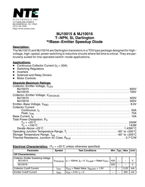
<strong>MJ10015</strong> & <strong>MJ10016</strong>T−NPN, <strong>Si</strong>, <strong>Darlington</strong>w /Base−Emitter Speedup DiodeDescription:The <strong>MJ10015</strong> and <strong>MJ10016</strong> are <strong>Darlington</strong> transistors in a TO3 type package designed for high−voltage, high−speed, power switching in inductive circuits where fall time is critical. They are particularlysuited for line operated switch−mode applications.Applications: Continuous Collector Current (I C = 50A) Switching Regulators Inverters Solenoid and Relay Drivers Motor ControlsAbsolute Maximum Ratings:Collector−Emitter Voltage, V CEV<strong>MJ10015</strong> . . . . . . . . . . . . . . . . . . . . . . . . . . . . . . . . . . . . . . . . . . . . . . . . . . . . . . . . . . . . . . . . . . . . . . 600V<strong>MJ10016</strong> . . . . . . . . . . . . . . . . . . . . . . . . . . . . . . . . . . . . . . . . . . . . . . . . . . . . . . . . . . . . . . . . . . . . . . 700VCollector−Emitter Voltage, V CEO(SUS)<strong>MJ10015</strong> . . . . . . . . . . . . . . . . . . . . . . . . . . . . . . . . . . . . . . . . . . . . . . . . . . . . . . . . . . . . . . . . . . . . . . 400V<strong>MJ10016</strong> . . . . . . . . . . . . . . . . . . . . . . . . . . . . . . . . . . . . . . . . . . . . . . . . . . . . . . . . . . . . . . . . . . . . . . 500VEmitter−Base Voltage, V EBO . . . . . . . . . . . . . . . . . . . . . . . . . . . . . . . . . . . . . . . . . . . . . . . . . . . . . . . . 8.0VCollector CurrentContinuous, I C . . . . . . . . . . . . . . . . . . . . . . . . . . . . . . . . . . . . . . . . . . . . . . . . . . . . . . . . . . . . . . . 50APeak, I CM . . . . . . . . . . . . . . . . . . . . . . . . . . . . . . . . . . . . . . . . . . . . . . . . . . . . . . . . . . . . . . . . . . . 75ABase Current, I B . . . . . . . . . . . . . . . . . . . . . . . . . . . . . . . . . . . . . . . . . . . . . . . . . . . . . . . . . . . . . . . . . . . 10ATotal Power Dissipation, P DT C = +25°C . . . . . . . . . . . . . . . . . . . . . . . . . . . . . . . . . . . . . . . . . . . . . . . . . . . . . . . . . . . . . . . . 250WT C = +100°C . . . . . . . . . . . . . . . . . . . . . . . . . . . . . . . . . . . . . . . . . . . . . . . . . . . . . . . . . . . . . . . 143WDerate Above +25°C . . . . . . . . . . . . . . . . . . . . . . . . . . . . . . . . . . . . . . . . . . . . . . . . . . . . . . . . 1.43W/°COperating Junction Temperature Range, T j . . . . . . . . . . . . . . . . . . . . . . . . . . . . . . . . . . −65° to +200°CStorage Temperature Range, T stg . . . . . . . . . . . . . . . . . . . . . . . . . . . . . . . . . . . . . . . . . . −65° to +200°CThermal Resistance, Junction−to−Case, R thJC . . . . . . . . . . . . . . . . . . . . . . . . . . . . . . . . . . . . . 0.7°C/WElectrical Characteristics: (T C = +25°C unless otherwise specified)Parameter Symbol Test Conditions Min Typ Max UnitOff CharacteristicsCollector−Emitter Sustaining Voltage<strong>MJ10015</strong> V CEO(SUS) I C = 100mA, I B = 0, V CLAMP = Rated V CEO 400 − − V<strong>MJ10016</strong>500 − − VCollector Cutoff Current I CEV V CEV = Rated Value, V BE(OFF) = 1.5V − − 0.25 mAEmitter Cutoff Current I EBO V EB = 2.0V, I c = 0 − − 350 mA
Electrical Characteristics (Cont’d): (T C = +25°C unless otherwise specified)Parameter Symbol Test Conditions Min Typ Max UnitOn Characteristics (Note 1)DC Current Gain h FE I c = 20A, V CE = 5.0V 25 − −I c = 40A, V CE = 5.0V 10 − −Collector−Emitter Saturation Voltage V CE(sat) I C = 20A, I B = 1.0A − − 2.2 VI C = 50A, I B = 10A − − 5.0 VBase−Emitter Saturation Voltage V BE(sat) I C = 20A, I B = 1.0A − − 2.75 VDiode Forward Voltage V F I F = 20A − − 5.0 VDynamic CharacteristicsOutput Capacitance C ob V CB = 10V, I E = 0, f = 100kHz − − 750 pFSwitching CharacteristicsDelay Time t d V CC = 250V, I C = 20A, I B1 = 1.0A,Rise Time t r V BE(off) = 5V, tp = 25µs, Duty Cycle ≤ 2%− − 0.3 us− − 1.0 usStorage Time t s − − 2.5 usFall Time t f − − 1.0 usNote 1. Pulse Test: Pulse width = 300µs, Duty Cycle ≤ 2%..135 (3.45) Max.350 (8.89).875 (22.2)Dia MaxSeatingPlaneC.312 (7.93) Min.040 (1.02)BEmitter1.187 (30.16) 50 8E.215 (5.45).665(16.9).156 (3.96) Dia(2 Holes).430(10.92).188 (4.8) R MaxBase.525 (13.35) R MaxCollector/Case