NTE3045 Optoisolator Silicon NPN Darlington Phototransistor Output
NTE3045 Optoisolator Silicon NPN Darlington Phototransistor Output
NTE3045 Optoisolator Silicon NPN Darlington Phototransistor Output

You also want an ePaper? Increase the reach of your titles
YUMPU automatically turns print PDFs into web optimized ePapers that Google loves.
<strong>NTE3045</strong><strong>Optoisolator</strong><strong>Silicon</strong> <strong>NPN</strong> <strong>Darlington</strong> <strong>Phototransistor</strong> <strong>Output</strong>Description:The <strong>NTE3045</strong> is a gallium arsenide LED optically coupled to a <strong>Silicon</strong> Photo <strong>Darlington</strong> transistor ina 6–Lead DIP type package designed for applications requiring electrical isolation, high breakdownvoltage, and high current transfer ratios. Characterized for use as telephone relay drivers but providesexcellent performance in interfacing and coupling systems, phase and feedback controls, solidstate relays, and general purpose switching circuits.Features: High Sensitivity to Low Input Drive Current High Collector–Emitter Breakdown Voltage: V (BR)CEO = 80V (Min) High Input–<strong>Output</strong> Isolation Guaranteed: V ISO = 7500V (Peak)Absolute Maximum Ratings: (T A = +25°C, unless otherwise specified)Input LEDReverse Voltage, V R . . . . . . . . . . . . . . . . . . . . . . . . . . . . . . . . . . . . . . . . . . . . . . . . . . . . . . . . . . . . . . . . . 3VContinuous Forward Current, I F . . . . . . . . . . . . . . . . . . . . . . . . . . . . . . . . . . . . . . . . . . . . . . . . . . . . 60mALED Power Dissipation (T A = +25°C with Negligible Power in <strong>Output</strong> Detector), P D . . . . . . 120mWDerate Above 25°C . . . . . . . . . . . . . . . . . . . . . . . . . . . . . . . . . . . . . . . . . . . . . . . . . . . . 1.41mW/°C<strong>Output</strong> DetectorCollector–Emitter Voltage, V CEO . . . . . . . . . . . . . . . . . . . . . . . . . . . . . . . . . . . . . . . . . . . . . . . . . . . . . . 80VEmitter–Collector Voltage, V ECO . . . . . . . . . . . . . . . . . . . . . . . . . . . . . . . . . . . . . . . . . . . . . . . . . . . . . . . 5VDetector Power Dissipation (T A = +25°C with Negligible Power in Input LED), P D . . . . . . . . 150mWDerate Above 25°C . . . . . . . . . . . . . . . . . . . . . . . . . . . . . . . . . . . . . . . . . . . . . . . . . . . . 1.76mW/°CTotal DeviceIsolation Surge Voltage (Peak AC Voltage, 60Hz, 1sec Duration, Note 1), V ISO . . . . . . . . . . . 7500VTotal Device Power Dissipation (T A = +25°C), P D . . . . . . . . . . . . . . . . . . . . . . . . . . . . . . . . . . . . 250mWDerate Above 25°C . . . . . . . . . . . . . . . . . . . . . . . . . . . . . . . . . . . . . . . . . . . . . . . . . . . . 2.94mW/°COperating Temperature Range, T A . . . . . . . . . . . . . . . . . . . . . . . . . . . . . . . . . . . . . . . . . . –55° to +100°CStorage Temperature Range, T stg . . . . . . . . . . . . . . . . . . . . . . . . . . . . . . . . . . . . . . . . . . –55° to +150°CLead Temperature (During Soldering for 10sec, 1/16” from Case), T L . . . . . . . . . . . . . . . . . . +260°CNote 1. Isolation surge voltage is an internal device dielectric breakdown rating. For this test, Pin1and Pin2 are common, and Pin4, Pin5, and Pin6 are common.
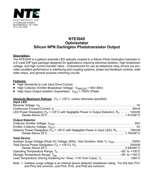
Electrical Characteristics: (T A = +25°C unless otherwise specified)Input LEDParameter Symbol Test Conditions Min Typ Max UnitReverse Leakage Current I R V R = 3V – 0.05 10 µAForward Voltage V F I F = 10mA – 1.15 2.0 VCapacitance C V R = 0, f = 1MHz – 18 – pFPhotodarlington (T A = +25°C, I F = 0 unless otherwise specified)Collector–Emitter Dark Current I CEO V CE = 60V – – 1 µACollector–Emitter Breakdown Voltage V (BR)CEO I C = 1mA 80 – – VEmitter–Collector Breakdown Voltage V (BR)ECO I E = 100µA 5 – – VCoupled (T A = +25°C unless otherwise specified)Collector <strong>Output</strong> Current I C V CE = 1.5V, I F = 10mA 50 – – mAIsolation Surge Voltage V ISO 60Hz Peak AC, 5sec, 7500 – – VNote 2, Note 3Isolation Resistance R ISO V = 500V, Note 2 – 10 11 – ΩIsolation Capacitance C ISO v = 0, f = 1MHz, Note 2 – 0.2 – pFSwitchingTurn–On Time t on V CC = 10V,R ΩTurn–Off Time t L = 100Ω,off I F = 5mARise Time t r– 3.5 – µs– 95 – µs– 1 – µsFall Time t f – 2 – µsNote 2. For this test LED Pin1 and Pin2 are common and <strong>Phototransistor</strong> Pin4 and Pin5 are common.Note 3. Isolation Surge Voltage, V ISO , is an internal device dielectric breakdown rating.Pin Connection Diagram65 41 2 3.260(6.6)MaxAnode16N.C..070 (1.78) MaxCathode25Collector.350 (8.89)Max.300 (7.62)N.C.34Emitter.200 (5.08)Max.350(8.89)Max.085 (2.16) Max.100 (2.54)