Signal Simulation in Folding and Interpolating Integrated ADC
Signal Simulation in Folding and Interpolating Integrated ADC
Signal Simulation in Folding and Interpolating Integrated ADC

Create successful ePaper yourself
Turn your PDF publications into a flip-book with our unique Google optimized e-Paper software.
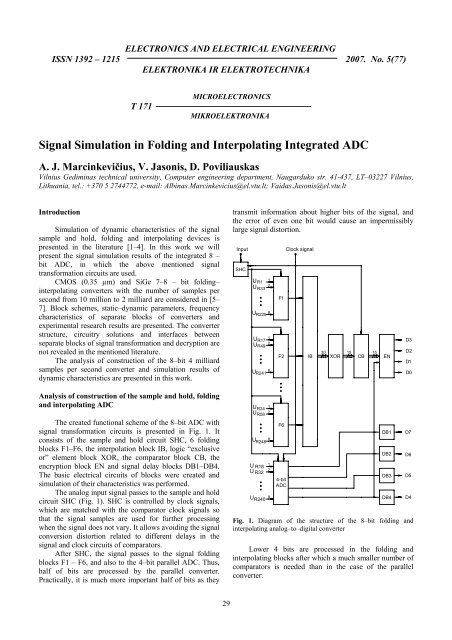
ELECTRONICS AND ELECTRICAL ENGINEERINGISSN 1392 – 1215 2007. No. 5(77)ELEKTRONIKA IR ELEKTROTECHNIKAMICROELECTRONICST 171 ────────────────────────MIKROELEKTRONIKA<strong>Signal</strong> <strong>Simulation</strong> <strong>in</strong> Fold<strong>in</strong>g <strong>and</strong> Interpolat<strong>in</strong>g <strong>Integrated</strong> <strong>ADC</strong>A. J. Marc<strong>in</strong>kevičius, V. Jasonis, D. PoviliauskasVilnius Gedim<strong>in</strong>as technical university, Computer eng<strong>in</strong>eer<strong>in</strong>g department, Naugarduko str. 41-437, LT–03227 Vilnius,Lithuania, tel.: +370 5 2744772, e-mail: Alb<strong>in</strong>as.Marc<strong>in</strong>kevicius@el.vtu.lt; Vaidas.Jasonis@el.vtu.ltIntroduction<strong>Simulation</strong> of dynamic characteristics of the signalsample <strong>and</strong> hold, fold<strong>in</strong>g <strong>and</strong> <strong>in</strong>terpolat<strong>in</strong>g devices ispresented <strong>in</strong> the literature [1–4]. In this work we willpresent the signal simulation results of the <strong>in</strong>tegrated 8 –bit <strong>ADC</strong>, <strong>in</strong> which the above mentioned signaltransformation circuits are used.CMOS (0.35 µm) <strong>and</strong> SiGe 7–8 – bit fold<strong>in</strong>g–<strong>in</strong>terpolat<strong>in</strong>g converters with the number of samples persecond from 10 million to 2 milliard are considered <strong>in</strong> [5–7]. Block schemes, static–dynamic parameters, frequencycharacteristics of separate blocks of converters <strong>and</strong>experimental research results are presented. The converterstructure, circuitry solutions <strong>and</strong> <strong>in</strong>terfaces betweenseparate blocks of signal transformation <strong>and</strong> decryption arenot revealed <strong>in</strong> the mentioned literature.The analysis of construction of the 8–bit 4 milliardsamples per second converter <strong>and</strong> simulation results ofdynamic characteristics are presented <strong>in</strong> this work.Analysis of construction of the sample <strong>and</strong> hold, fold<strong>in</strong>g<strong>and</strong> <strong>in</strong>terpolat<strong>in</strong>g <strong>ADC</strong>The created functional scheme of the 8–bit <strong>ADC</strong> withsignal transformation circuits is presented <strong>in</strong> Fig. 1. Itconsists of the sample <strong>and</strong> hold circuit SHC, 6 fold<strong>in</strong>gblocks F1–F6, the <strong>in</strong>terpolation block IB, logic “exclusiveor” element block XOR, the comparator block CB, theencryption block EN <strong>and</strong> signal delay blocks DB1–DB4.The basic electrical circuits of blocks were created <strong>and</strong>simulation of their characteristics was performed.The analog <strong>in</strong>put signal passes to the sample <strong>and</strong> holdcircuit SHC (Fig. 1). SHC is controlled by clock signals,which are matched with the comparator clock signals sothat the signal samples are used for further process<strong>in</strong>gwhen the signal does not vary. It allows avoid<strong>in</strong>g the signalconversion distortion related to different delays <strong>in</strong> thesignal <strong>and</strong> clock circuits of comparators.After SHC, the signal passes to the signal fold<strong>in</strong>gblocks F1 – F6, <strong>and</strong> also to the 4–bit parallel <strong>ADC</strong>. Thus,half of bits are processed by the parallel converter.Practically, it is much more important half of bits as theytransmit <strong>in</strong>formation about higher bits of the signal, <strong>and</strong>the error of even one bit would cause an impermissiblylarge signal distortion.InputSHCU R1U R3312U R2258U R17U R4912U8 R241U R24U R5612U 8 R248U R18U R3212U 8 R240F1F2F64-bit<strong>ADC</strong>Clock signalIB30 1515XOR CBENDB2DB3DB4D3D2D1D0DB1 D7Fig. 1. Diagram of the structure of the 8–bit fold<strong>in</strong>g <strong>and</strong><strong>in</strong>terpolat<strong>in</strong>g analog–to–digital converterLower 4 bits are processed <strong>in</strong> the fold<strong>in</strong>g <strong>and</strong><strong>in</strong>terpolat<strong>in</strong>g blocks after which a much smaller number ofcomparators is needed than <strong>in</strong> the case of the parallelconverter.D6D5D429
Fig. 2. Time diagrams of <strong>in</strong>put <strong>and</strong> output signals of the 8–bit fold<strong>in</strong>g – <strong>in</strong>terpolat<strong>in</strong>g <strong>ADC</strong>Both the 4–bit parallel comparator <strong>and</strong> the fold<strong>in</strong>gblocks (F1 – F6) are switched to the reference voltageformation circuit <strong>in</strong> a certa<strong>in</strong> order.From fold<strong>in</strong>g blocks the signals pass to the<strong>in</strong>terpolat<strong>in</strong>g circuit block <strong>and</strong> then together with signals ofhigher bits – to the decod<strong>in</strong>g circuit blocks. The 8–bitb<strong>in</strong>ary signal is obta<strong>in</strong>ed <strong>in</strong> the decoder output.<strong>Simulation</strong> of characteristics of the fold<strong>in</strong>g –<strong>in</strong>terpolat<strong>in</strong>g converterThe ma<strong>in</strong> parameters of the simulated converter arepresented <strong>in</strong> Table 1.Table 1. Parameters of the sample <strong>and</strong> hold, fold<strong>in</strong>g <strong>and</strong><strong>in</strong>terpolat<strong>in</strong>g <strong>ADC</strong>.Frequency of the converter analog s<strong>in</strong>e signal (0–100) MHzNumber of b<strong>in</strong>ary bits8 bitsFrequency of the converter clock pulses 4 GHzAmplitude of the analog s<strong>in</strong>e signal1.6 VSupply voltage of the converter3.3 VFold<strong>in</strong>g coefficient 8Interpolation coefficient 6M<strong>in</strong>imal dimension of technology 0.5 µmcorrespond<strong>in</strong>g to the bipolar transistor modelparametersTime diagrams of <strong>in</strong>put <strong>and</strong> output signals of the 8–bit fold<strong>in</strong>g – <strong>in</strong>terpolat<strong>in</strong>g <strong>ADC</strong> are presented <strong>in</strong> Fig. 2. In thefigure there are also presented:u IN () t is the simulated <strong>in</strong>put signal, the frequency ofwhich is 10 MHz;D0 – D7 are <strong>ADC</strong> digital outputs correspond<strong>in</strong>g tothe b<strong>in</strong>ary code, where D7 is the output of the highest bit,<strong>and</strong> D0 is the output of the lowest bit;*u ODI( t)is „DAC imitation output“ – the signalsimulated by the package P–Spice accord<strong>in</strong>g to equations(1) <strong>and</strong> (2).For the simulation of the converter electric circuits bythe program package P–Spice the parameters of the 0.5 µmtechnology bipolar transistor models were used.When simulat<strong>in</strong>g a full <strong>ADC</strong> system with sample <strong>and</strong>hold, fold<strong>in</strong>g <strong>and</strong> <strong>in</strong>terpolation circuits, it is important tocompare the <strong>in</strong>put signal with the signal which wasreproduced accord<strong>in</strong>g to the output 8–bit b<strong>in</strong>ary code ofthe converter. For this purpose a digital–to–analogconverter should be used. In this work we simulate theDAC function by the P–Spice package us<strong>in</strong>g an empiricalequation (1):u( t) = uD0( t) + 2 uD1( t) + 4uD2( t) + 8uD ( t)+u ( t) + 32u( t) + 64u( t) u ( t)ODI 3+ 16 D4 D5D6+ 128 D7, (1)here u ODI ( t)is the DAC „imitation“ output voltage;u D0– uD7are the digital output voltages of the simulated<strong>ADC</strong>.In Fig. 2, alongside with the <strong>in</strong>put s<strong>in</strong>e signal thesignal reproduced from the b<strong>in</strong>ary code D0–D7 ispresented, which is calculated by the follow<strong>in</strong>g empiricalequation:u*ODI() t() tuODI= −U, (2)032here0 U = 23,5 V.As it can be seen <strong>in</strong> Fig. 2, the analog signalreproduced from the <strong>ADC</strong> output b<strong>in</strong>ary code agrees wellwith the <strong>in</strong>put s<strong>in</strong>e signal. Pulse peaks <strong>in</strong> the reproduced30
s<strong>in</strong>e signal appear due to <strong>in</strong>accuracies of compatibility of<strong>ADC</strong> delay circuits.By simulat<strong>in</strong>g the fold<strong>in</strong>g – <strong>in</strong>terpolat<strong>in</strong>g <strong>ADC</strong> thetime characteristics of output signals D0–D7 were alsoobta<strong>in</strong>ed at different <strong>in</strong>put analog signal frequencies (5, 10,15, 20, 30, 40, 50, 100, 500, 1000 MHz). The timecharacteristics of the converter output signals at 10, 20,<strong>and</strong> 40 MHz are shown <strong>in</strong> Fig. 4–6.These characteristics show that the change range ofthe b<strong>in</strong>ary code 8–output signals is from 3.1 to 3.3 V at<strong>in</strong>put signal frequencies up to f max = 10 MHz. By further<strong>in</strong>creas<strong>in</strong>g the frequency, the pulse amplitudes of lowestbits decrease (Fig. 5, 6).Hav<strong>in</strong>g analyzed time diagrams of the converteroutput signal, the dependence of the effective number ofbits change on the frequency of the <strong>in</strong>put analog signal wasdeterm<strong>in</strong>ed (Fig. 3).to voltages, we still see that the error is not exceeded.Thus, the number of effective bits is equal to 8 bits.Fig. 5. <strong>ADC</strong> output signals at the 20 MHz <strong>in</strong>put frequencyFig. 3. Dependence of the effective number of bits (ENOB) onthe <strong>in</strong>put signal frequency fThe characteristic <strong>in</strong> Fig. 3 shows that the effectivenumber of bits of the created fold<strong>in</strong>g – <strong>in</strong>terpolat<strong>in</strong>gconverter is 8 bits at the <strong>in</strong>put signal maximum frequencyof 10 MHz. By <strong>in</strong>creas<strong>in</strong>g the <strong>in</strong>put signal frequency, thenumber of effective bits decreases <strong>and</strong> the accuracy of 6bits is obta<strong>in</strong>ed at the <strong>in</strong>put signal frequency of 50 MHz.The frequency can be improved by us<strong>in</strong>g transistor modelsof more advanced technology (SiGe or CMOS 0.35 µm) orby reduc<strong>in</strong>g the fold<strong>in</strong>g <strong>and</strong> <strong>in</strong>terpolation coefficients.Fig. 4. <strong>ADC</strong>S output signals at the 10 MHz <strong>in</strong>put frequencyAs it can be seen <strong>in</strong> Fig. 4, all eight digital outputsignals fit <strong>in</strong>to the range from 3.1 to 3.3 V. Bypredeterm<strong>in</strong><strong>in</strong>g the underst<strong>and</strong>able error of 10 % accord<strong>in</strong>gFig. 6. <strong>ADC</strong> output signals at the 40 MHz <strong>in</strong>put frequencyBy simulat<strong>in</strong>g by computer with the Pentium 4processor, the clock frequency of which is 3 GHz <strong>and</strong>RAM of 1 GB, one cycle of the transient processsimulation lasted about 8 hours when calculat<strong>in</strong>g a full<strong>in</strong>put signal s<strong>in</strong>usoid (Fig. 2) <strong>and</strong> about 1 hour whencalculat<strong>in</strong>g short time periods (Fig. 4–6).ConclusionsThe structure of the fold<strong>in</strong>g <strong>and</strong> <strong>in</strong>terpolat<strong>in</strong>g analog–to–digital converter was created, which <strong>in</strong>cludes the signalsample <strong>and</strong> hold, fold<strong>in</strong>g <strong>and</strong> <strong>in</strong>terpolat<strong>in</strong>g circuits, theelectric schemes of which are formed on the basis ofbipolar silicon transistors.The methodology of simulat<strong>in</strong>g dynamiccharacteristics of the 8–bit b<strong>in</strong>ary converter was developedas well as dynamic characteristics of the converter withsignal transformation circuits were simulated <strong>and</strong>parameters were <strong>in</strong>vestigated.It has been determ<strong>in</strong>ed that the maximum number ofbits per second of such a converter reaches 4·10 9 , <strong>and</strong> thenumber of effective bits is 8 when the analog signalmaximum frequency is 10 MHz. By <strong>in</strong>creas<strong>in</strong>g the analogsignal frequency, the number of effective bits decreases<strong>and</strong> it is equal to 4 at 100 MHz. The analog signalmaximum frequency of the fold<strong>in</strong>g – <strong>in</strong>terpolat<strong>in</strong>g <strong>ADC</strong>31
can be <strong>in</strong>creased by reduc<strong>in</strong>g the fold<strong>in</strong>g <strong>and</strong> <strong>in</strong>terpolat<strong>in</strong>gcoefficients. The <strong>in</strong>vestigation has shown that when the<strong>in</strong>terpolation coefficient is K = 4 <strong>and</strong> the fold<strong>in</strong>gcoefficient is M = 3, the analog signal f max for the 8–bitconverter can be about 1 GHz. The converter speed would<strong>in</strong>crease by improv<strong>in</strong>g parameters of the transistor models.References1. Marc<strong>in</strong>kevičius A., Jasonis V. Analog<strong>in</strong>ės atm<strong>in</strong>tiesschemos parametrų skaičiavimas signalo laikymo veikoje //Elektronika ir elektrotechnika. – Kaunas: Technologija, 2006.– Nr. 2 (66). – P. 31 – 35.2. Jasonis V., Poviliauskas D., Marc<strong>in</strong>kevičius A. <strong>Simulation</strong>of the <strong>Integrated</strong> <strong>Signal</strong> Fold<strong>in</strong>g Circuit with P–Spice //Electronics <strong>and</strong> Electrical Eng<strong>in</strong>eer<strong>in</strong>g. – Kaunas:Technologija, 2007. – No. 1 (73). – P. 37 – 40.3. Marc<strong>in</strong>kevičius A., Jasonis V. Calculation of InterpolationParameters <strong>in</strong> the Comparator Analog Information Converters// Electronics <strong>and</strong> Electrical Eng<strong>in</strong>eer<strong>in</strong>g. – Kaunas:Technologija, 2006. – No. 5 (69). – P. 5 – 8.4. Marc<strong>in</strong>kevičius A., Jasonis V. The Calculation of DynamicErrors <strong>in</strong> <strong>Signal</strong> Transformation Circuits of Analog – to –Digital Converters for Mechatronic Systems // Solid StatePhenomena. – Trans Tech Publications, Switzerl<strong>and</strong>, 2006. –Vol. 113. – P. 131 – 136.5. Vessal F., Salama C. A. T. An 8–Bit 2–Gsample/s Fold<strong>in</strong>g–Interpolat<strong>in</strong>g Analog–to–Digital Converter <strong>in</strong> SiGeTechnology // IEEE Journal of Solid – State Circuits, 2004. –Vol. 39, No. 1. – P. 238 – 241.6. Li Y., Sanchez–S<strong>in</strong>encio E. A Wide Input B<strong>and</strong>width 7–bit300–Msample/s Fold<strong>in</strong>g <strong>and</strong> Current–Mode Interpolat<strong>in</strong>g<strong>ADC</strong> // IEEE Journal of Solid – State Circuits, 2003. – Vol.38. – No. 8. – P. 1405 – 1410.7. Liu M. H., Liu S. I. An 8–bit 10 MS/s Fold<strong>in</strong>g <strong>and</strong>Interpolat<strong>in</strong>g <strong>ADC</strong> Us<strong>in</strong>g the Cont<strong>in</strong>ous–Time Auto–ZeroTechnique // IEEE Journal of Solid – State Circuits, 2001. –Vol. 36. – No. 1. – P. 122 – 128.Submitted for publication 2007 03 21A. J. Marc<strong>in</strong>kevičius, V. Jasonis, D. Poviliauskas. <strong>Signal</strong> <strong>Simulation</strong> <strong>in</strong> Fold<strong>in</strong>g <strong>and</strong> Interpolat<strong>in</strong>g <strong>Integrated</strong> <strong>ADC</strong> // Electronics<strong>and</strong> Electrical Eng<strong>in</strong>eer<strong>in</strong>g. – Kaunas: Technologija, 2007. – No. 5(77). – P. 29–32.The structure of the fold<strong>in</strong>g <strong>and</strong> <strong>in</strong>terpolat<strong>in</strong>g analog-to-digital converter, which <strong>in</strong>cludes the signal sample <strong>and</strong> hold, fold<strong>in</strong>g <strong>and</strong><strong>in</strong>terpolat<strong>in</strong>g circuits, the electric circuits of which are formed on the basis of silicon bipolar transistors of the 0.5 µm technology, ispresented. The methodology of simulation of dynamic characteristics of the created 8-b<strong>in</strong>ary bit converter <strong>and</strong> calculation of the digitaloutput signal form was developed. The results of simulation of dynamic characteristics of the converter with signal transformationcircuits <strong>and</strong> <strong>in</strong>vestigation of frequency parameters are presented. It has been determ<strong>in</strong>ed that the maximum number of samples persecond of such a converter reaches 4·10 9 , <strong>and</strong> the number of effective bits with the analog signal maximum frequency of 10 MHz is 8. Ithas been shown that by <strong>in</strong>creas<strong>in</strong>g the analog signal frequency the number of effective bits of the converter decreases <strong>and</strong> at the 50 MHzfrequency it is equal to 6. The <strong>in</strong>vestigations have shown that the analog signal maximum frequency of the fold<strong>in</strong>g-<strong>in</strong>terpolat<strong>in</strong>g <strong>ADC</strong>can be <strong>in</strong>creased by reduc<strong>in</strong>g the fold<strong>in</strong>g <strong>and</strong> <strong>in</strong>terpolation coefficients. When the <strong>in</strong>terpolation coefficient is K = 4 <strong>and</strong> the fold<strong>in</strong>gcoefficient is M = 3, the analog signal f max for the 8-bit converter could be about 1 GHz. Ill. 6, bibl. 7. (<strong>in</strong> English; summaries <strong>in</strong> English,Russian <strong>and</strong> Lithuanian).А. И. Марцинкявичюс, В. Ясонис, Д. Повиляускас. Моделирование сигналов в интегральном свёрточноинтерполяционном АЦП // Электроника и электротехника. – Каунас: Технология, 2007. – № 5(77) . – С. 29–32.Приведена структура свёрточно интерполяционного АЦП (СИАЦП), в состав которого входит устройство выборки ихранения, схемы свёртки и интерполяции сигнала. Электрические схемы разработаны на биполярных транзисторах спараметрами моделей при 0,5 микронной технологии. Создана методика моделирования динамических характеристик ирасчета сигналов восьмиразрядного СИАЦП. Представлены результаты исследования частотных характеристик и основныхточностных параметров такого АЦП. Показано, что максимальная частота выборки достигает 4 ГГц, и при частоте аналоговогосигнала 10 МГц обеспечивается восьмиразрядная точность преобразования. Установлено, что при увеличении максимальнойчастоты аналогового сигнала точность преобразования уменьшается и при частоте 50 МГц падает до 6 разрядов. Исследованияпоказали, что дальнейшее увеличение быстродействия СИАЦП возможно при уменьшении коэффициентов свёртки иинтерполяции цепей трансформации аналогового сигнала. При коэффициенте интерполяции K = 4 и коэффициенте свёртки M= 3, восьмиразрядная точность может быть получена при максимальной частоте аналогового сигнала около одного ГГц. Ил. 6,библ. 7 (на английском языке; рефераты на английском, русском и литовском яз.).A. J. Marc<strong>in</strong>kevičius, V. Jasonis, D. Poviliauskas. <strong>Signal</strong>ų modeliavimas sąsūkos ir <strong>in</strong>terpoliacijos <strong>in</strong>tegr<strong>in</strong>iame ASK //Elektronika ir elektrotechnika. – Kaunas: Technologija, 2007. – Nr. 5(77). – P. 29–32.Pateikta sąsūkos ir <strong>in</strong>terpoliacijos analog<strong>in</strong>io-skaitmen<strong>in</strong>io keitiklio s<strong>and</strong>ara. Į jį įe<strong>in</strong>a signalų imties ir laikymo, sąsūkos ir<strong>in</strong>terpoliacijos gr<strong>and</strong>ynai, kurių elektr<strong>in</strong>ės schemos sudarytos silicio dvipolių tranzistorių pagr<strong>in</strong>du, esant 0,5 mikrometro technologijai.Sudaryta sukurto 8 dvejeta<strong>in</strong>ių skilčių keitiklio d<strong>in</strong>am<strong>in</strong>ių charakteristikų modeliavimo ir skaitmen<strong>in</strong>ių išėjimo signalų formosskaičiavimo metodika. Pateikti keitiklio su signalo transformacijos gr<strong>and</strong><strong>in</strong>ėmis d<strong>in</strong>am<strong>in</strong>ių charakteristikų modeliavimo ir dažn<strong>in</strong>iųparametrų tyrimo rezultatai. Parodyta, kad tokio keitiklio maksimalus imčių skaičius per sekundę siekia 4·10 9 , o efektyviųjų bitųskaičius, kai analog<strong>in</strong>io signalo maksimalus dažnis 10 MHz, lygus aštuoniems. Parodyta, kad, did<strong>in</strong>ant analog<strong>in</strong>io signalo dažnį,keitiklio efektyviųjų bitų skaičius mažėja ir, esant 50 MHz, lygus 6. Tyrimais nustatyta kad sąsūkos ir <strong>in</strong>terpoliacijos ASK analog<strong>in</strong>iosignalo maksimalų dažnį galima padid<strong>in</strong>ti maž<strong>in</strong>ant sąsūkos ir <strong>in</strong>terpoliacijos koeficientus. Esant <strong>in</strong>terpoliacijos koeficientui K = 4 irsąsūkos koeficientui M = 3, analog<strong>in</strong>io signalo f max 8 bitų keitikliui galėtų būti apie 1 GHz. Il. 6, bibl. 7 (anglų kalba; santraukos anglų,rusų ir lietuvių k.).32