An Integrated CMOS Chaos Generator
An Integrated CMOS Chaos Generator
An Integrated CMOS Chaos Generator

You also want an ePaper? Increase the reach of your titles
YUMPU automatically turns print PDFs into web optimized ePapers that Google loves.
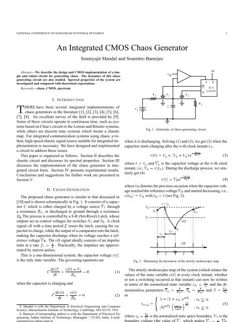
NATIONAL CONFERENCE ON NONLINEAR SYSTEMS & DYNAMICS 1<strong>An</strong> <strong>Integrated</strong> <strong>CMOS</strong> <strong>Chaos</strong> <strong>Generator</strong>Soumyajit Mandal and Soumitro BanerjeeAbstract—We describe the design and <strong>CMOS</strong> implementation of a simpleand robust circuit for generating chaos. The dynamics of this chaosgenerating circuit are also studied. Spectral properties of the system areinvestigated and compared with theoretical expectations.Keywords—chaos, <strong>CMOS</strong>, spectrumI. INTRODUCTIONÌHERE have been several integrated implementations ofchaos generators in the literature [1], [2], [3], [4], [5], [6],[7], [8]. <strong>An</strong> excellent survey of the field is provided by [9].Some of these circuits operate in continuous time, such as systemsbased on Chua’s circuit or the Lorenz and Rössler systems,while others are discrete time systems which iterate a chaoticmap. For integrated communication systems using chaos, a robust,high-speed chaotic signal source suitable for integrated implementationis necessary. We have designed and implementeda circuit to address these issues.This paper is organized as follows. Section II describes thechaotic circuit and discusses its spectral properties. Section IIIdiscusses the implementation of the chaos generator in integratedcircuit form. Section IV presents experimental results.Conclusions and suggestions for further work are presented inSection V.II. CHAOS GENERATIONThe proposed chaos generator is similar to that discussed in[10] and is shown schematically in Fig. 1. It consists of a capacitorC which is either charged by a voltage source ν througha resistance ʽ, or discharged to ground through a resistanceʾ.The process is controlled by a S-R (Set-Reset) Latch, whoseoutputs act as control voltages for switches ˽ and ˾. A clocksignal clk with a time period Ì resets the latch, causing the capacitorto charge, while the output of a comparator sets the latch,making the capacitor discharge when its voltage reaches a referencevoltage Î Ê . The clk signal ideally consists of an impulsetrain at a rate ½ . Practically, the impulses are approximatedby narrow pulses.ÌThis is a one-dimensional system; the capacitor voltage ڴصis the only state variable. The governing equations are dڴصdØ· ڴص Î ½Ê½when the capacitor is charging and dڴصdØ· ڴصʾ¼ (1)¼ (2)S. Mandal is with the Department of Electrical Engineering and ComputerScience, Massachusetts Institute of Technology, Cambridge, MA 02139, USAS. Banerjee (Corresponding author) is with the Department of Electrical Engineering,Indian Institute of Technology, Kharagpur - 721302, India, E-mail:V1+−R1clkV −R+S RQR−SQ LATCHS1S2CR2Fig. 1. Schematic of chaos-generating circuit.when it is discharging. Solving (1) and (2), we get (3) when thecapacitor starts charging after the Ò-th clock instant Ø Ò .ڴص ν ´Î½ Î Ò µ e Ø ØÒÊ ½ (3)where ØØ Ò and Î Ò is the capacitor voltage at the Ò-th clockinstant, i.e., Î Ò Ú´Ø Ò µ. During the discharge process, we similarlyget (4)ڴص Î Ê e Ø Ø Ê Ê¾ (4)where Ø Ê denotes the previous occasion when the capacitor voltagereached the reference voltage Î Ê and started decreasing, i.e.,Ú´Ø Ê µÎ Ê with Ø Ê Ø(see Fig. 2).VVRbVn-1tn1t = tTRtn2Vnv(t)Fig. 2. Illustrating the derivation of the strictly stroboscopic map.The strictly stroboscopic map of the system (which relates thevalues of the state variable ڴص at every clock instant, whetheror not a switching occurred at that instant) can now be writtenin terms of the normalized state variable Þ Ò ÎÒ and the dimensionlessparameters ̽ asÞ Ò·½ clkTVÌʽ , Ì ¾ ½ ´½ Þ Ò µ e ̽¬e ̾ ½ ÞÒ½ ¬ Ì ¾Ì ½n+1tÌÊ¾Î½Þ Ò Þ and ¬ ÎÊÎ½Þ Ò Þ (5)where Þ Î Î½ is the normalized state space boundary. Î is the
2 NATIONAL CONFERENCE ON NONLINEAR SYSTEMS & DYNAMICSi.e., Ø Ò¾ ¼in Fig. 2), and Þ divides the normalized state spaceinto two parts. It is given byÞ ½ ´½ ¬µ e ̽ (6)Fig. 3(a) shows the structure of the map for ̽ ¼¾, ̾ ½¼and ¬ ¼. The map is piecewise smooth: it has two parts,separated by the state space boundary at Þ (6). The left handpart is linear with a slope e ̽ , while the right hand part is nonlinear.The fixed point Þ Ò·½ Þ Ò is unstable, and can exhibitchaos for some ranges of the parameters ̽, ̾, and ¬ [11].Typical bifurcation diagrams are shown in Figs. 3(b), 3(c) and3(d). Several period doubling and border-collision bifurcationsare clearly seen. The invariant density ´Þµ of the map is shownin Fig. 4 for ̽ ¼¾, ̾ ½¼ and ¬ ¼.In Figs. 3(c) and 3(d), the chaotic region expands as Ì ½ decreasesand the slope e ̽ of the left hand part of (5) approachesunity. In the limit as ̽ ¼, there are no periodic windows inFigs. 3(c) and 3(d) and the chaos generator satisfies the conditionsfor robust chaos given in [12]. This is desirable for oursystem since it reduces sensitivity to parameter fluctuations.Ì00 0.2 0.4 0.6 0.8 1 1.2 1.4 1.6 1.8 2tained theoretically for Ð ½ MHz, ¿ pF, f / f clkFig. 5.chaotic waveform used for spreading (above) and ڴص (below).32.8502.62.4402.22301.81.6200 2 4 6 8 10 12 14 16 18 20f (MHz)1.4501.210.25 0.3 0.35 0.4 0.45 0.5z0.55 0.6 0.65 0.7 0.7540Fig. 4. Invariant density ´Þµ of the strictly stroboscopic map for Ì ½ ¼¾,Ì ¾ ½¼ and ¬ ¼.30A simple way to obtain a binary valued chaotic waveform200 2 4 6 8 10 12 14 16 18 20from the circuit is to use Q or Q, the outputs of the S-R (Set-f (MHz)Reset) latch (see Fig. 1). Binary chaotic sequences are alternativesto real valued waveforms for spreading digital data inspread spectrum communication systems using chaos. In thiscase, since Q is low whenever the capacitor charges and is highwhenever it discharges, the voltage ´Øµ at Q is a quantized (binaryvalued) version of the capacitor voltage ڴص and has goodIII. VLSI IMPLEMENTATIONautocorrelation properties when ڴص is chaotic. Correlations betweennearby chips decay exponentially fast; typical correlationdecay times are less than ¿Ì . If required, these correlations canbe further reduced by sub sampling.<strong>An</strong> advantage of this chaotic circuit is that its power spectraldensity can be readily calculated using (3) and (4) and ensembleaveraging [13]. Fig. 5 compares the theoretical power spectraldensities of ڴص and ´Øµ obtained using this method.Fig. 6 compares the power spectral densities of the chaoticlatch output signal ´Øµ obtained experimentally with that ob-ρ(z)PSD (dB)605040302010PSD of d(t)PSD of v(t)Comparing the power spectral densities of ´Øµ, the binary valuedThus ̽ ¼¾, ̾ ¼¼ and ¬ ¼. Both spectra weresampled at 40 MHz. By comparing them, we conclude that wewere able to predict the main features of the experimental spectrumwith good accuracy.PSD (dB)PSD (dB)Fig. 6. Comparing experimental (above) and theoretical (below) power spectraldensities of ´Øµ, the binary valued chaotic waveform used for spreading,with Ð ½ MHz in both cases.A schematic of the integrated chaos generator is shown inFig. 7. This circuit is a straightforward <strong>CMOS</strong> adaptation ofthe one shown in Fig. 1. Device sizes are given in Table I. <strong>An</strong> n-well process was used, and hence all NMOS devices have theirbulks grounded. PMOS devices have bulks shorted to sourcesto avoid body bias effects (bulk connections are not shown inFig. 7).The comparator is a single-ended two-stage design. Its outputis fed to a <strong>CMOS</strong> inverter, which acts as a buffer and improvesthe slew rate. Simulated comparator slew rates were about 25V/sec. The maximum operational frequency of the circuit is
INDIAN INSTITUTE OF TECHNOLOGY, KHARAGPUR 721302, DECEMBER 28-30, 2003 30.750.70.650.60.55z n+10.50.450.40.350.30.250.25 0.3 0.35 0.4 0.45 0.5 0.55 0.6 0.65 0.7 0.75z n(a)(b)(c)(d)Fig. 3. The strictly stroboscopic map and its bifurcations. (a) Strictly stroboscopic map for Ì ½ ¼¾, Ì ¾ ½¼ and ¬ ¼. Bifurcation diagrams of the mapwith respect to (b) Ì ½ for Ì ¾ ½and ¬ ¼; (c) Ì ¾ for Ì ½ ¼¾ and ¬ ¼; (d) ¬ for Ì ½ ¼¾ and Ì ¾ ½.TABLE ITRANSISTOR SIZING FOR FIG.7Device(s) Size (W/L, m)M1 1.6/1M2 1/1M3,M4 14.5/1M5,M6 40/1M7,M8 2.25/1M9 23.5/1M10 77.5/1M11 7.5/1M12 5/1M13,M14 19/0.25M15,M16 50/0.25IV.In this implementation, ʽ, ʾ, , ν, Î Ê and ¬ are the sameas in Fig. 6. The ratio ̽ ʾ was fixed at 0.31, but the̾ ʽclock frequency ( Ð ½ µ was kept variable to evaluate systemÌEXPERIMENTAL RESULTSThe chaos generator was laid out in a n-well, single-poly, fivemetalstandard digital <strong>CMOS</strong> process with a minimum featuresize of 0.25 m. A micro-photograph of the integrated chaosgenerator is shown in Fig. 8.The chip was tested using a 2.5 V power supply. Fig. 9 showsthe output waveform ڴص from the integrated chaos-generatingcircuit with Ð =14.8 MHz. The Lyapunov exponent obtainedfrom time series data is positive, indicating chaos. Ð was variedand chaotic behavior was observed from 10 MHz to 16 MHz.This corresponds to the parameters ̽ and ̾ varying over theranges (0.41, 0.26) and (1.32, 0.83), respectively. Thus the circuit’schaotic behavior is robust to parameter fluctuations of over40%. Fig. 10 shows the chaotic binary sequence ´Øµ obtainedfrom the chaos generator for Ð =15.2 MHz.V. CONCLUSIONSWe have described the analysis, design and implementation
4 NATIONAL CONFERENCE ON NONLINEAR SYSTEMS & DYNAMICSVddM7M8I BIAS M9 M11 S-R LATCHM1v(t)S QM5 M6V R+ − VM15M141M2R QclkM3M4 M10 M12COMPARATORR 2M13M16R 1d(t)CFig. 7. Schematic of chaos generator.Fig. 9. Chaotic waveform ڴص obtained from the integrated chaos generator for Ð =14.8 MHz (0.5 V/div, 1 s/div).Fig. 10. Chaotic binary sequence ´Øµ obtained from the integrated chaos generator Ð =15.2 MHz (1 V/div, 400 ns/div).Fig. 8. Chip micro-photograph of integrated chaos generator.a small on-chip area and is suitable for integrated realization ofchaotic communication systems. The circuit has been built andtested and its functionality verified.ACKNOWLEDGMENTSWe would like to thank Abhishek Somani for help with designand layout, the Advanced VLSI Design Laboratory, IndianInstitute of Technology, Kharagpur for CAD tools and NationalSemiconductor Corporation for providing fabrication facilities.REFERENCES[1] A. Rodríguez-Vázquez and M. Delgado-Restituto, “<strong>CMOS</strong> design ofchaotic oscillators using state variables: A monolithic Chua’s circuit,”IEEE Trans. Circuits Syst. II, vol. 40, no. 10, pp. 596–613, Oct. 1993.[2] M. Delgado-Restituto and A. Rodríguez-Vázquez, “Design considerationsfor integrated continuous-time chaotic oscillators,” IEEE Trans. CircuitsSyst. I, vol. 45, no. 4, pp. 481–495, Apr. 1998.[3] M. Delgado-Restituto, M. Li nán, and A. Rodríguez-Vázquez, “<strong>CMOS</strong>2.4m chaotic oscillator: Experimental verification of chaotic encryptionof audio,” Elec. Lett., vol. 32, pp. 795–796, Apr. 1996.[4] Octavio A. Gonzalez, “VLSI implementation of a chaotic encryption algorithmwith applications to secure communications,” Master’s thesis, Texas[5] M. Delgado-Restituto and A. Rodríguez-Vázquez, “Mixed-signal mapconfigurableintegrated chaos generator for chaotic communications,”IEEE Trans. Circuits Syst. I, vol. 48, no. 12, pp. 1462–1474, Dec. 2001.[6] A. Dornbusch and J. P. De Gyvez, “Chaotic generation on PN sequences:a VLSI implementation,” Proc. IEEE Int. Symp. Circuits and Systems(ISCAS ’99), vol. 5, pp. 454–457, 1999.[7] T. Morie, S. Sakabayashi, M. Nagata, and A. Iwata, “<strong>CMOS</strong> circuits generatingarbitrary chaos by using pulsewidth modulation techniques,” IEEETrans. Circuits Syst. I, vol. 47, no. 11, pp. 1652–1657, Nov. 2000.[8] A. S. Elwakil, K. N. Salama, and M. P. Kennedy, “<strong>An</strong> equation for generatingchaos and its monolithic implementation,” Int. Journal Bifurcationand <strong>Chaos</strong>, vol. 12, no. 12, pp. 2885–2985, Dec. 2002.[9] M. Delgado-Restituto and A. Rodríguez-Vázquez, “<strong>Integrated</strong> chaos generators,”Proc. IEEE, vol. 90, no. 5, pp. 747–767, 2002.[10] T. Kousaka, T. Kido, T. Ueta, H. Kawakami, and M. Abe, “<strong>An</strong>alysis ofborder-collision bifurcation in a simple circuit,” Proc. IEEE Int. Symp.Circuits and Systems (ISCAS ’00), vol. 2, pp. 481–484, May 2000.[11] S. Banerjee, M. S. Karthik, G. Yuan, and J. A. Yorke, “Bifurcations in onedimensionalpiecewise smooth maps - theory and applications in switchingcircuits,” IEEE Trans. Circuits Syst. I, vol. 47, no. 3, pp. 389–393, Mar.2000.[12] S. Banerjee, J. A. Yorke, and C. Grebogi, “Robust chaos,” Phys. Rev. Lett.,vol. 80, pp. 3049–3052, 1998.[13] O. Woywode, J. Weber, H. Güldner, A. Baranovski, and W. Schwarz, “Statisticalanalysis of chaotic DC-DC converters,” Proc. Int. Conf. Energy,Automation and Information Technology (EAIT ’01), Dec. 2001.