Design Challenges in HBT MMIC Amplifier Bias Circuits
Design Challenges in HBT MMIC Amplifier Bias Circuits
Design Challenges in HBT MMIC Amplifier Bias Circuits

Create successful ePaper yourself
Turn your PDF publications into a flip-book with our unique Google optimized e-Paper software.
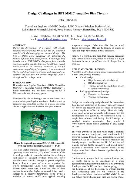
<strong>Design</strong> <strong>Challenges</strong> <strong>in</strong> <strong>HBT</strong> <strong>MMIC</strong> <strong>Amplifier</strong> <strong>Bias</strong> <strong>Circuits</strong>John D BirkbeckConsultant Eng<strong>in</strong>eer – <strong>MMIC</strong> <strong>Design</strong>, RFIC Group – Wireless Bus<strong>in</strong>ess Unit,Roke Manor Research Limited, Roke Manor, Romsey, Hampshire, SO51 0ZN, UKDirect Telephone +44(0)1794 833143. Fax: +44(0)1794 833433Email: john.birkbeck@roke.co.uk Website: http://www.roke.co.ukABSTRACTDur<strong>in</strong>g the development of a custom <strong>HBT</strong> <strong>MMIC</strong>,solutions will be evolved for the RF and DC circuits <strong>in</strong>parallel with the packag<strong>in</strong>g and thermal design. Thetype of <strong>MMIC</strong> be<strong>in</strong>g developed will determ<strong>in</strong>e therelative difficulty these areas present. Follow<strong>in</strong>g a brief<strong>in</strong>troduction to <strong>HBT</strong> <strong>MMIC</strong>s, this paper focuses on theissues associated with the design of the DC bias circuit,which need to be correctly addressed if the fullperformance capability of the process is to be unlocked.Merits and disadvantages of basic and advanced biasschemes are discussed for circuits target<strong>in</strong>g Class Athrough to Class AB operation.INTRODUCTIONHetero-junction Bipolar Transistor (<strong>HBT</strong>) MonolithicMicrowave Integrated Circuit (<strong>MMIC</strong>) technology isfirmly established and has been serv<strong>in</strong>g the RF &Microwave <strong>in</strong>dustry for many years.Simplistically, the technology can be considered as ameans to <strong>in</strong>tegrate bipolar transistors, diodes, resistors,capacitors and <strong>in</strong>ductors together on a s<strong>in</strong>gle <strong>in</strong>tegratedcircuit. A typical <strong>MMIC</strong> is shown <strong>in</strong> Figure 1 below.Figure 1: A plastic packaged <strong>MMIC</strong> (lid removed),with support components, on an FR4 PCB.The high useful operat<strong>in</strong>g frequency (GHz) and highoperat<strong>in</strong>g current density (200µA/µm 2 ) features of thetechnology make it em<strong>in</strong>ently suitable for realis<strong>in</strong>g avast range of different products from low powermultifunctional circuits through to power amplifiers.From a designer’s po<strong>in</strong>t of view, an important factwhich dist<strong>in</strong>guishes GaAs <strong>HBT</strong>s from traditionalSilicon bipolar transistors, is that the ‘Vbe’ of thesedevices is somewhat higher at around 1.3V, and issubject to a negative temperature slope giv<strong>in</strong>g avariation of around ±0.1V over typical operat<strong>in</strong>gtemperature ranges. Other than this, from an <strong>in</strong>itialdesign perspective, <strong>HBT</strong>s can be thought of simply asvery fast, high performance bipolar transistors.F<strong>in</strong>ally, it is worth not<strong>in</strong>g here, that standard processesonly support NPN devices, which we will see is a majorlimitation <strong>in</strong> the scope of bias circuit design that ispossible.APPLICATION CHALLENGESAny <strong>HBT</strong> <strong>MMIC</strong> development requires consideration ofat least the follow<strong>in</strong>g elements:• Circuit design• High frequency electrical circuit• DC electrical circuit• Thermal circuit (ie modell<strong>in</strong>g effectsof device self heat<strong>in</strong>g)• Packag<strong>in</strong>g and assembly design• Electrical performance• Thermal performance<strong>Design</strong> can be relatively straightforward for cases wherethere is good headroom on the supply rail, only modestRF powers are required, and the circuit is allowed tooperate largely as a Class A design. Here, the designareas listed above are relatively <strong>in</strong>dependent, and thedevelopment can generally be undertaken us<strong>in</strong>g asimple bias scheme, and bas<strong>in</strong>g the RF design onstandard foundry s-parameter data, which ifrepresentative should almost guarantee 1 st pass designsuccess.The other extreme is the case where there is m<strong>in</strong>imalheadroom on the supply rail, and considerable RFpower is required from devices, necessitat<strong>in</strong>g operationnearer to Class B to achieve comb<strong>in</strong>ed efficiency andl<strong>in</strong>earity targets. In this case, the RF, DC and thermalcircuits become highly <strong>in</strong>teractive, and circuit designbecomes a potentially more iterative process as thedesign areas listed above become significantly more<strong>in</strong>terdependent.One important means to limit this unwanted <strong>in</strong>teraction,to enable design to be undertaken <strong>in</strong> a moredeterm<strong>in</strong>istic and less iterative manner, is by appropriatedevelopment of the DC base bias circuit topology.For the purposes of this discussion, we will say that themost demand<strong>in</strong>g case we will consider is thedevelopment of a bias circuit for an <strong>HBT</strong> <strong>MMIC</strong> for use<strong>in</strong> a battery powered equipment such as a mobile phone,
equired to run from an unregulated DC supply <strong>in</strong> the 3-4V region. Also, we would like to consider designoptions for both low power Class A circuits through tohigh power Class AB circuits.Start<strong>in</strong>g from the <strong>HBT</strong> shown <strong>in</strong> Figure 2 below, wewill develop basic base bias circuits, to highlight areaswhich present a particular design challenge. Means tomitigate these challenges will be proposed, and themerits and disadvantages discussed.This paper will conclude by show<strong>in</strong>g how this designknowledge can be used to develop alternative highperformance bias circuits, by us<strong>in</strong>g one of the authorspatent pend<strong>in</strong>g designs as an example.collector current to vary, <strong>in</strong> turn caus<strong>in</strong>g poor RF andDC performance. Secondly, if the transistor was a large‘power’ device, the current required from the basesupply may be of the order of tens of milliamps, whichdoes not lend itself to connection to a low power SiliconIC control circuit as may be typically used. F<strong>in</strong>ally, thissort of topology will not operate well as a so-called deepClass AB power amplifier, this class be<strong>in</strong>g required fora good efficiency/l<strong>in</strong>earity trade off <strong>in</strong> a mobile phonetransmit power amplifier (more on this shortly).Two approaches could be considered here for reduc<strong>in</strong>gthe circuit’s sensitivity to process, temperature andsupply rail. The classic approach of the addition of anemitter degeneration resistor would yield a serviceabletopology for very low power operation, as would the useof a current mirror, which works very well <strong>in</strong> an ICenvironment. These approaches are shown <strong>in</strong> Figure 4and Figure 5 respectively.Base DCSupplyCollectorDC Supply(optional L)RFoutFigure 2: <strong>HBT</strong> Transistor to biasRF<strong>in</strong>BASIC BIAS CIRCUIT DESIGNThe addition of a few components to the transistor ofFigure 2, takes us to one of the simplest forms of biascircuit possible shown <strong>in</strong> Figure 3 below.Base DC Supply0V /3.0V(±0.1V)Base <strong>Bias</strong>Resistor3-4VCollector DC SupplyCollector<strong>Bias</strong>ChokeRFoutFigure 4: <strong>Bias</strong> Stabilisation by emitter de-generationBase DC Supply Collector DC SupplyRFoutRF<strong>in</strong>DCBlockVbe = 1.3V ±0.1Vover temperatureDCBlockß = 50-100 overprocess &temperatureA=kR=rn(optional L)R=rA=knDCBlockFigure 3: A simple <strong>HBT</strong> bias circuitIn this case, the collector bias rema<strong>in</strong>s permanentlyconnected through the bias choke, and the circuit isactivated by a switched regulated DC voltage fed to thebase via a resistor, which also functions as an RF blockto some degree, additional series <strong>in</strong>ductance be<strong>in</strong>gadded to improve this if required. Leakage current <strong>in</strong><strong>HBT</strong>s is very low, and so permanent collector biasworks for most battery powered applications. Whilstthe base current <strong>in</strong>jected will rema<strong>in</strong> fairly <strong>in</strong>dependentof temperature and the modest supply rail variationsshown, this circuit suffers from a number of problems.Beta variation with process and temperature causes theRF<strong>in</strong>Figure 5: <strong>Bias</strong> stabilisation by current mirrorHowever, we are <strong>in</strong>terested <strong>in</strong> a develop<strong>in</strong>g a solutioncapable of use with power amplifiers too. So for thiscase, the next stage is to add DC buffer<strong>in</strong>g <strong>in</strong> the basebias feed. This is typically achieved by use of anemitter follower from the control l<strong>in</strong>e as shown <strong>in</strong>Figure 6. This improved circuit reduces the potentiallyhigh current demand from the regulated control l<strong>in</strong>e toan acceptable level by transferr<strong>in</strong>g most of the dra<strong>in</strong> tothe unregulated supply.
This circuit however has a new disadvantage over theorig<strong>in</strong>al circuit of Figure 3, <strong>in</strong> that we have run out ofvoltage headroom on our control l<strong>in</strong>e and our circuit isnow critically sensitive to temperature and supply railvariation, s<strong>in</strong>ce we are rely<strong>in</strong>g on generat<strong>in</strong>g a currentsource from a potential difference which may vary <strong>in</strong>this example from 0.1V to 0.7V across the bias resistor.RF<strong>in</strong>Base DCSupply0V /3.0V(±0.1V)Vbe = 1.3V ±0.1V0.1 to 0.7V !!!DCBlockBase<strong>Bias</strong>ResistorVbe = 1.3V ±0.1VCollector DC Supply3-4VCollector<strong>Bias</strong>ChokeDCBlockRFoutß = 50-100 overprocess &temperatureFigure 6: <strong>HBT</strong> bias circuit with DC bufferA variation factor of the order of seven is unacceptable,and some temperature and power rail compensation isrequired. The addition of two diodes and a resistoryields the circuit of Figure 8. This circuit relies on goodthermal coupl<strong>in</strong>g such that the diode voltage tracks Vbechanges with temperature, clamp<strong>in</strong>g the base voltage atthe emitter follower, reduc<strong>in</strong>g the circuit’s sensitivity.Before we leave the circuit of Figure 6, anotherimportant advantage needs to be described. Theaddition of the emitter follower transistor means that wenow have a circuit which can be tailored to provide aClass AB mode of operation. Class AB amplifierdesign is a subject <strong>in</strong> itself, so only a basic description isnecessary here, to highlight features of a bias circuit thatare needed to address this requirement:An aside: Class AB operation basicsIn Class AB, the circuit is set up so that <strong>in</strong> the absenceof an RF signal, the ma<strong>in</strong> transistor is biased at somelow quiescent collector current, such that for low RFdrive levels it functions as a l<strong>in</strong>ear amplifier. As the RFdrive level <strong>in</strong>creases, rectification causes the circuit toself-bias, and operation is more towards Class B. Thiscan be expla<strong>in</strong>ed with reference to Figure 7 below.Base DCSupply3.0VEmitterFollowerVxCollector DC Supply<strong>Bias</strong>ResistorAmpFigure 7: Class AB operationOn the forward current half cycle, Vx tends to riseslightly as the RF current drives the base of the ma<strong>in</strong>transistor. This clamps the base emitter voltage of theemitter follower, such that it does not supply current tothe ma<strong>in</strong> transistor. On the negative go<strong>in</strong>g half cycle,Vx drops, and the ‘return’ RF current is supplied fromthe emitter follower. The rectification which occursmeans the time averaged voltage at the base of the ma<strong>in</strong>transistor is lower than when the RF signal was absent,and its collector current is higher. In this way the circuitoperates as a deep Class AB design, and can ma<strong>in</strong>ta<strong>in</strong> amuch improved total battery efficiency over a widerange of operat<strong>in</strong>g powers, than could be achieved forClass A. It can readily be appreciated that the choice ofbias resistor will strongly <strong>in</strong>fluence the self bias<strong>in</strong>gprofile achieved, and <strong>in</strong>deed there is an optimum valuefor this component for different modulation schemesand l<strong>in</strong>earity requirements. In practice of course,additional challenges present themselves for goodoverall Class AB circuit design. However for thepurposes of this bias circuit discussion, the need to<strong>in</strong>corporate features to allow and tailor self bias<strong>in</strong>g hasbeen expla<strong>in</strong>ed.To summarise then, the circuit of Figure 6, has reducedcontrol current requirements, and an option for ClassAB operation.Base DCSupply0V /3.0V(±0.1V)RF<strong>in</strong>Base<strong>Bias</strong>ResistorCollector DC Supply3-4VDCBlockRFoutFigure 8: A circuit just suitable for provid<strong>in</strong>g deepClass AB bias for a ‘saturated’ modulation type PA.The circuit of Figure 8, with the previously describedcompensation diodes, is our first fully practical biascircuit, m<strong>in</strong>or variants of which may be found forexample <strong>in</strong> deep Class AB GSM <strong>HBT</strong> power amplifiers<strong>MMIC</strong>s sell<strong>in</strong>g <strong>in</strong> high volume.However, this circuit is not without its disadvantages.Whilst provid<strong>in</strong>g some thermal compensation, the biaspo<strong>in</strong>t may still vary by as much as a factor of three overa typical temperature range of -25°C to +80°C. Thecontrol current is rather high aga<strong>in</strong> (up to 15mA <strong>in</strong> somecases), due to the need to waste a certa<strong>in</strong> amount <strong>in</strong> thediode clamp. Next, whilst suitable for driv<strong>in</strong>g a poweramplifier <strong>in</strong> a Class AB mode for the case where asaturated modulation scheme is used, it is not suitablefor use with l<strong>in</strong>ear modulation schemes (CDMA etc),where unacceptable adjacent channel leakage wouldresult for adequately low quiescent currents. F<strong>in</strong>ally,
limitations <strong>in</strong> device models and CAD software, meansthis sort of circuit is difficult to design for 1 st passsuccess, and iterations of many variants may be neededto f<strong>in</strong>d the one that gives the best trade off betweenperformance and yield. It is essential, for mobile phonepower amplifiers <strong>in</strong> particular to optimise every last bitof performance from the smallest die possible, s<strong>in</strong>ceonly the very best components will sell successfully.From Figure 8, to take the next step <strong>in</strong> bias circuitdevelopment to achieve a circuit that works well withl<strong>in</strong>ear modulation and lower control currents, takes us tothe area of advanced bias circuit design, where manypatent applications can be found. This level of IPgeneration highlights the importance of a good biascircuit - it really is a major key to unlock<strong>in</strong>g theperformance of the target <strong>HBT</strong> process, for theapplication <strong>in</strong> hand.Read<strong>in</strong>g through these works reveals a surpris<strong>in</strong>g rangeof clearly dist<strong>in</strong>ct methods used to tackle the problem.On one extreme, solutions exist that use relativelysimple circuits comb<strong>in</strong><strong>in</strong>g the three basic forms ofbias<strong>in</strong>g we have discussed (resistive based, currentmirror based & emitter follower based). The topologyis configured to access the benefits of each yield<strong>in</strong>g acircuit that works well for high power l<strong>in</strong>ear modulationClass AB amplifiers. On the other extreme, solutionscan be found which are based on more complex circuitsus<strong>in</strong>g multiple current mirrors or a control loopapproach. Whilst more complex <strong>in</strong> terms of the numberof components, these solutions are still adequatelycompact on-chip. F<strong>in</strong>ally, to augment these schemes,modifications to the standard <strong>HBT</strong> process areoccasionally made. Such modifications <strong>in</strong>clude specialultra-compact low frequency transistors for the biascircuit, or changes to the metalisation arrangements forbetter thermal performance.Before such an advanced bias scheme is discussed, it isappropriate to summarise the key po<strong>in</strong>ts of thediscussion so far:Why is proper design of the bias circuit topology soimportant?• To unlock the full performance potential of the<strong>HBT</strong> process• To improve the ‘designability’ of the circuit toreduce development costsWhat are the design issues?• Need to optimise the bias circuit <strong>in</strong>teraction withthe RF signal• Need a power down function• May need high power / low power modes & l<strong>in</strong>ear /saturated modes• Need m<strong>in</strong>imum current draw from regulated controll<strong>in</strong>es.• Need good process, supply and temperaturetolerance• Need a compact on-chip implementationWhy are these issues difficult?• Some solutions require large on-chip componentssuch as <strong>in</strong>ductors to ma<strong>in</strong>ta<strong>in</strong> l<strong>in</strong>earity, and soreduce the cost effectiveness of the design.• A switched 0/2.8V ‘enable’ control l<strong>in</strong>e is typicallyavailable. NPN devices only, means that it isdifficult to design a topology with a power downmode, with low control current draw <strong>in</strong> the on-state.• A bias circuit with different modes is difficult todesign without compromis<strong>in</strong>g some aspect ofperformance.• Emerg<strong>in</strong>g high performance processes offer<strong>in</strong>g a‘ß’ circa three times higher than conventional <strong>HBT</strong>will mean suppliers us<strong>in</strong>g conventional technologyand simple bias circuits only could eventually beforced from the market.• High Vbe=1.3V, compared to supply rail typically3.0V makes useful circuits <strong>in</strong>volv<strong>in</strong>g stackeddevices impossible.• High Vbe <strong>in</strong> comb<strong>in</strong>ation with low Vcc and typicaltemperature coefficients, can lead to poor stabilityover temperature.ADVANCED BIAS CIRCUIT DESIGNThe previous section developed simple bias topologiesby sequentially add<strong>in</strong>g components until the requiredfunctionality was achieved, and then add<strong>in</strong>g furthercomponents to correct additional problems that arosealong the way.The understand<strong>in</strong>g that this process has provided, assummarised <strong>in</strong> the bullet po<strong>in</strong>ts above, is a necessaryprecursor to enable more advanced topologies as used <strong>in</strong>the <strong>in</strong>dustry, to be designed.As an example, the development of one such bias circuitas undertaken by the author will now be discussed. Theaim was to generate a bias circuit that could beconfigured either for Class A operation or for deepClass AB operation and allow for ready modification to<strong>in</strong>clude additional features such as switched bias po<strong>in</strong>ts.Also, and very importantly, to reduce the circuit’ssensitivity to process, temperature and supply railvariation not only <strong>in</strong> f<strong>in</strong>al hardware, but also at thedesign stage, such that the circuit could be simulatedus<strong>in</strong>g exist<strong>in</strong>g CAD software and models with improvedcorrelation to measurement.As an R&D consultant to the <strong>MMIC</strong> <strong>in</strong>dustry,ownership of such a circuit by the RFICs Group at RokeManor Research Limited was clearly highly desirable.Figure 9 below conta<strong>in</strong>s the elements which wereasserted to be essential for the aims targeted. The ma<strong>in</strong>RF transistor (bottom right) is permanently connectedvia the collector circuit to the supply rail which mayvary from 3.0V at the end of the batteries life up to 6.0Vwhen on-charge. An emitter follower is essential tom<strong>in</strong>imise the current drawn from the regulated controll<strong>in</strong>e, which is now shown as the more typical 0/2.8V. Asmall mirror transistor, <strong>in</strong> close thermal coupl<strong>in</strong>g to the
ma<strong>in</strong> transistor, provides accurate monitor<strong>in</strong>g of thequiescent condition <strong>in</strong> the transistor. From this startpo<strong>in</strong>t, additional circuitry is required to somehowconvert the low level ‘sensed’ current <strong>in</strong> the mirrortransistor <strong>in</strong>to an ‘error’ current that can be used to pullthe emitter follower’s base node down, such that thecircuit reaches the desired equilibrium.Vctrl =2.8V ±0.1VVpdDropperResistorsEmitterFollowerVcc = 3.0V to 6.0VTR1CollectorCircuit &BaseFeedbackRFout+circuit which aside from the <strong>in</strong>itial reference currentgeneration relies wholly on component ratios. Also, itwill be appreciated that the circuit offers good immunityto supply rail variation, s<strong>in</strong>ce any such variation causesnear equal change <strong>in</strong> both sense and reference voltages.Vctrl =2.8V ±0.1VRxIref1IntermediateReferenceVoltageIntermediateSense VoltageIsense1RxMirrorTransistorVpdDropperResistorsEmitterFollowerMirrorTransistorActiveRFPowerCellCurrentSett<strong>in</strong>gResistorIerrorFigure 11: Addition of a reference current generatorRF<strong>in</strong>Figure 9: Essential Elements for the exampleadvanced bias circuit discussionAs may be anticipated, the topology is beg<strong>in</strong>n<strong>in</strong>g to looklike one of the “control circuit” types mentioned earlier,one miss<strong>in</strong>g element clearly be<strong>in</strong>g a reference signal ofsome sort. The desired control loop concept <strong>in</strong> this caseis summarised <strong>in</strong> Figure 10 below.The relative comparison and conversion to an errorsignal was the most difficult problem to overcome,although as often seems the case with circuit topologydevelopment, the solution actually appears quite simple.The function is achieved us<strong>in</strong>g a current mirror and onefurther transistor to provide a Vbe reference and DCamplification of the error. The loop is then closed, asshown <strong>in</strong> Figure 12 below.Vctrl =2.8V ±0.1VReferenceCurrentSenseCurrentMirrorTransistorVpdDropperResistorsEmitterFollowerThe f<strong>in</strong>al stage is to add a power down switch andadditional diode to block a leakage path. This completecircuit is shown <strong>in</strong> Figure 13 below. Despite theapparent large quantity of components, thisimplementation is very compact on chip, s<strong>in</strong>ce most ofthe additional transistors are near to m<strong>in</strong>imum size forprocess, and most of the resistors can be made verynarrow and short. Such resistors are more prone tomanufactur<strong>in</strong>g spread, but s<strong>in</strong>ce the circuit primarilydepends on ratios rather than absolute values, this canbe well tolerated.IerrorVctrl =2.8V ±0.1VVpdDropperResistorsFigure 10: Control Circuit ConceptA reference current generator can readily be designedus<strong>in</strong>g another emitter follower as shown <strong>in</strong> Figure 11below. This sets up a reference current <strong>in</strong> the collector,determ<strong>in</strong>ed by a s<strong>in</strong>gle resistor <strong>in</strong> the emitter arm toground. The temperature coefficient of this resistor canoften be made equal and opposite to that of Vbe, suchthat the current produced is <strong>in</strong>dependent of temperatureand varies only with the regulation of the Vpd l<strong>in</strong>e.RxCurrentSett<strong>in</strong>gResistorIntermediateReferenceVoltageIref1Isense2CurrentSubtractorRyx 1MirrorIntermediateSense VoltageRyIref2Isense1RxMirrorTransistorIref2-Isense2IerrorError<strong>Amplifier</strong>EmitterFollowerAddition of equal resistors <strong>in</strong> the collector arm of thistransistor, and the orig<strong>in</strong>al mirror transistor, convertsthese sense and reference currents <strong>in</strong>to voltages.Provid<strong>in</strong>g we can f<strong>in</strong>d a way to perform a relativecomparison between these levels, then we have a niceFigure 12: Addition of the differential currentcomparator and error amplifier.
Vctrl =2.8V ±0.1VCurrentSett<strong>in</strong>gResistorRxIntermediateReferenceVoltageIref1Isense2CurrentSubtractorRyx 1MirrorIntermediateSense VoltageSwitchRyIref2Isense1MirrorTransistorIref2-Isense2RxVpdDropperResistorsIerrorError<strong>Amplifier</strong>Vcc = 3.0V to 6.0V+TR1CollectorEmitter Circuit &Follower BaseFeedbackRFoutRF<strong>in</strong>ActiveRFPowerCellS<strong>in</strong>gle Mode<strong>Bias</strong> Circuit forClass AB PAOn-chip Componentsshown. M<strong>in</strong>imum off-chipdecoupl<strong>in</strong>g caps alsorequiredFigure 13: Essentially complete circuit, provid<strong>in</strong>gbias for Class AB Power Amplification.All bias circuits tend to have some natural thermalslope, which causes a drift <strong>in</strong> quiescent bias level <strong>in</strong> onedirection with temperature. Generally, a positive slopeis desired to help achieve the same RF output power athigher temperature. The natural slope of this circuit is<strong>in</strong> the correct direction, and can actually be tailored asrequired. It was also found that parameters such asadjacent channel power ratio and 3 rd order <strong>in</strong>tercept canbe optimised with m<strong>in</strong>imal impact on other circuitparameters, which is an extremely useful feature.F<strong>in</strong>ally to note that additional modifications are possibleto realise switched quiescent po<strong>in</strong>ts, such as would berequired for a dual mode amplifier required to operatewith either l<strong>in</strong>ear or saturated modulation schemes.Altogether then, this circuit addressed and overcame allof the key issues, and with m<strong>in</strong>imum additionalcapacitors off-chip can be made to work nicely as a biassolution for l<strong>in</strong>ear Class AB amplifiers.To remove the self bias<strong>in</strong>g feature, a s<strong>in</strong>gle capacitorcan be added across the base emitter junction of theemitter follower. This serves to make the emitterfollower a near open circuit to RF, and very l<strong>in</strong>earamplification <strong>in</strong> Class A results.Overall this topology proved to be a great success, thefeatures and benefits be<strong>in</strong>g summarised as follows:• Configurability for deep Class AB through to ClassA. All configurations maximise RF performance,especially l<strong>in</strong>earity.• Power down and other modes can be supported.• Ultra low current draw from control l<strong>in</strong>es, typically80% lower than other <strong>in</strong>dustry solutions• Excellent process, supply and temperature tolerance– by design.• Excellent ‘designablility’ – s<strong>in</strong>gle componentchanges largely affect one design parameter only.• Compact on-chip <strong>in</strong>ductorless implementation• Inherently designed for high manufactur<strong>in</strong>g yieldon any <strong>HBT</strong> process.• Excellent process transportabilitySUMMARYThe importance of good bias circuit design for <strong>HBT</strong><strong>MMIC</strong>s has been expla<strong>in</strong>ed, and the key issues that needto be considered have been made clear, throughexamples of simple circuits. This basic knowledgeprimer is necessary for anyone wish<strong>in</strong>g to design a moreadvanced topology.One such topology is the author’s patent pend<strong>in</strong>gconfigurable bias circuit, and by way of example itsdevelopment has been described. This circuit wasshown to address the key issues raised, and can beconfigured for either Class A or deep Class AB. In allconfigurations the circuit offers very low process,temperature and supply rail sensitivity, giv<strong>in</strong>g improvedyield <strong>in</strong> f<strong>in</strong>al hardware, and improved ‘designablility’ atthe development stage, enabl<strong>in</strong>g 1 st pass design successfor challeng<strong>in</strong>g design specifications to be more readilyachieved, than would be possible with more primitivedesigns.REFERENCESThis paper refers to circuit and techniques as described<strong>in</strong> the patent applications: GB0304053, GB0306405,PCT/GB03/01167, & PCT/GB03/01309.CAUTIONARY NOTEIt must be mentioned that anyone plann<strong>in</strong>g to release an<strong>HBT</strong> <strong>MMIC</strong> product, would be well advised to conducta thorough patent search <strong>in</strong> advance for aspects of thedesign, such as bias circuit topology.FURTHER INFORMATIONThe reader is <strong>in</strong>vited to visit our website athttp://www.roke.co.uk for further <strong>in</strong>formation on <strong>HBT</strong><strong>Bias</strong> <strong>Circuits</strong>, and general <strong>MMIC</strong> and RF ASICactivities at Roke Manor. In particular, the follow<strong>in</strong>gdatasheets can be downloaded:• http://www.roke.co.uk/download/datasheets/hbt_mmic_design.pdf• http://www.roke.co.uk/download/datasheets/hbt_bias_circuit.pdf• http://www.roke.co.uk/download/datasheets/mmic_design_consultancy.pdfAlternatively please phone Technical Information on+44(0)1794 833000.© 01/10/03 - Roke Manor Research Ltd.