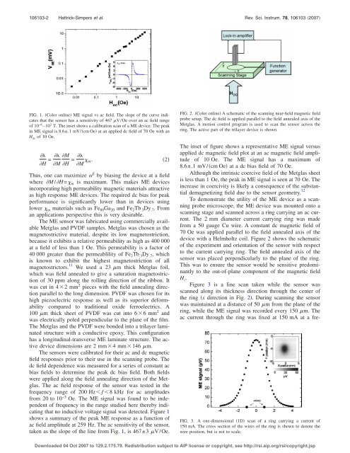
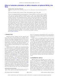
106103-2 Hattrick-Simpers et al. Rev. Sci. Instrum. 78, 106103 2007FIG. 1. Color online ME signal vs ac field. The slope <strong>of</strong> the curve indicatesthat the sensor has a sensitivity <strong>of</strong> 467 V/Oe over an ac field range<strong>of</strong> 10 −6 –10 3 T. The inset shows a calibration scan <strong>of</strong> a ME device. The peakin ME signal is 8.6±.1 mV/cm Oe at an applied dc field <strong>of</strong> 70 Oe with anH ac <strong>of</strong> 10 Oe.H = MM H = M m.Thus, one can maximize E by biasing the device at a fieldwhere M /H= m is maximum. This makes ME devicesincorporating high permeability magnetic materials attractiveas high response ME devices. The required dc bias for peakperformance is significantly lower than in devices usinglower m materials such as Fe 80 Ga 20 and Fe 2 Tb .3 Dy .7 . Froman applications perspective this is very desirable.The ME sensor was fabricated using commercially availableMetglas and PVDF samples. Metglas was chosen as themagnetostrictive material, despite its low magnetostriction,because it exhibits a relative permeability as high as 400 000at a field <strong>of</strong> less than 1 Oe. This permeability is a factor <strong>of</strong>40 000 greater than the permeablility <strong>of</strong> Fe 2 Tb .3 Dy .7 , whichis known to exhibit the highest magnetostriction <strong>of</strong> allmagnetostrictors. 11 We used a 23 m thick Metglas foil,which was field annealed to give a saturation magnetostriction<strong>of</strong> 30 ppm along the rolling direction <strong>of</strong> the ribbon. Itwas cut in 42 mm 2 pieces with the field annealing directionparallel to the long dimension. PVDF was chosen for itshigh piezoelectric response as well as its superior deformabilitycompared to traditional oxide ferroelectrics. A100 m thick sheet <strong>of</strong> PVDF was cut into 66 mm 2 andwas electrically poled perpendicular to the plane <strong>of</strong> the film.The Metglas and the PVDF were bonded into a trilayer laminatedstructure with a conductive epoxy. This configurationhas a longitudinal-transverse ME laminate structure. The activedevice dimensions are 2 mm4 mm146 m.The sensors were calibrated for their ac and dc magneticfield responses prior to their use in the <strong>scanning</strong> <strong>probe</strong>. Thedc field dependence was measured for a series <strong>of</strong> constant acbias fields to determine the peak dc bias field. Both fieldswere applied along the field annealing direction <strong>of</strong> the Metglas.The ac field response <strong>of</strong> the sensor was tested in thefrequency range <strong>of</strong> 200 Hz f 8 kHz for ac amplitudesfrom 20 to 10 −5 Oe. The ME signal was found to be independent<strong>of</strong> frequency in the range studied here thereby indicatingthat no inductive voltage signal was detected. Figure 1shows a summary <strong>of</strong> the peak ME response as a function <strong>of</strong>ac field amplitude at 259 Hz. The ac sensitivity <strong>of</strong> the sensor,taken as the slope <strong>of</strong> the line from Fig. 1, is467±3V/Oe.2FIG. 2. Color online A schematic <strong>of</strong> the <strong>scanning</strong> near-field magnetic field<strong>probe</strong> setup. The dc field is applied parallel to the field annealed axis <strong>of</strong> theMetglas. A motion control program is used to scan the sensor across thering. The active part <strong>of</strong> the trilayer device is shown.The inset <strong>of</strong> figure shows a representative ME signal versusapplied dc magnetic field plot at an ac magnetic field amplitude<strong>of</strong> 10 Oe. The ME signal has a maximum <strong>of</strong>8.6±.1 mV/cm Oe at a dc bias field <strong>of</strong> 70 Oe.Although the intrinsic coercive field <strong>of</strong> the Metglas sheetis less than 1 Oe, the peak in ME signal is seen at 70 Oe. Theincrease in coercivity is likely a consequence <strong>of</strong> the substantialdemagnetizing field due to the sensor geometry. 12To demonstrate the utility <strong>of</strong> the ME device as a <strong>scanning</strong><strong>probe</strong> microscope, the ME device was mounted onto a<strong>scanning</strong> stage and scanned across a ring carrying an ac current.The 2 mm diameter current carrying ring was madefrom a 50 gauge Cu wire. A constant dc magnetic field <strong>of</strong>70 Oe was applied parallel to the field annealed axis <strong>of</strong> thedevice with a Helmholtz coil. Figure 2 shows the schematic<strong>of</strong> the experiment and orientation <strong>of</strong> the sensor with respectto the current carrying ring. The field annealed axis <strong>of</strong> thesensor was placed perpendicularly to the plane <strong>of</strong> the ring.This was to ensure the sensor would be sensitive predominantlyto the out-<strong>of</strong>-plane component <strong>of</strong> the magnetic fieldH z .Figure 3 is a line scan taken while the sensor wasscanned along its thickness direction through the center <strong>of</strong>the ring x direction in Fig. 2. During <strong>scanning</strong> the sensorwas maintained at a distance <strong>of</strong> 50 m from the plane <strong>of</strong> thering, while the ME signal was recorded every 150 m. Theac current through the ring was fixed at 150 mA at a fre-FIG. 3. A one-dimensional 1D scan <strong>of</strong> a ring carrying a current <strong>of</strong>150 mA. The cross section <strong>of</strong> the wires <strong>of</strong> the ring is shown to denote thewire position, but is not to scale.Downloaded 04 Oct 2007 to 129.2.175.79. Redistribution subject to AIP license or copyright, see http://rsi.aip.org/rsi/copyright.jsp
106103-3 Notes Rev. Sci. Instrum. 78, 106103 2007FIG. 4. A series <strong>of</strong> line scans taken for different I ac through the ring. Thedata have been multiplied by 1, 5, and 30 for 15 mA, 1.5 mA, and 150 A,respectively. The cross section <strong>of</strong> the wires <strong>of</strong> the ring is shown to denotethe wire position, but is not to scale.quency <strong>of</strong> 5 kHz. The position <strong>of</strong> the ring wire cross sectionsrelative to the signal is denoted in the figure by the blackcircles.Looking closely at the line scan from Fig. 3, andtaking into consideration the dimensions <strong>of</strong> our device146 m2 mm4 mm and a <strong>scanning</strong> height <strong>of</strong> 50 m,the measured magnetic field displays a broadened pr<strong>of</strong>ile.The discrepancy results from the fact that 1 in any nearfield<strong>scanning</strong> device the spatial resolution is comparable tothe device dimension, and 2 the magnetic permeability <strong>of</strong>the Metglas is distorting the magnetic field distribution <strong>of</strong> thering over the dimensions <strong>of</strong> the device.A finite element analysis, using the s<strong>of</strong>tware FEMM,was performed not shown here to confirm that the presence<strong>of</strong> the Metglas alters the field distribution <strong>of</strong> a current carryingwire, and that the extent to which the field redistributiontakes place is <strong>of</strong> the order <strong>of</strong> the device size. To examinethe possible effect <strong>of</strong> the extremely high permeability <strong>of</strong>Metglas, calculations were performed for materials with=400 000 as well as =40. We found that the degree towhich the field redistribution takes place and the length scaleover which it occurs were comparable in both cases.The local field distortion present in near-field <strong>scanning</strong>magnetic <strong>probe</strong> techniques using magnetic sensors is known.For instance, in MFM, the interaction between the magnetictip and sample surface is known to affect the local field distribution.To accurately and precisely interpret the images,significant postmeasurement deconvolution involving detailedknowledge <strong>of</strong> tip geometry and magnetic properties isrequired. 13,14 The active sensing area that needs to be modeledfor deconvolution in MFM studies is <strong>of</strong> the order <strong>of</strong> thetip dimensions. Similarly, in the present magnetic trilayerdevice, field redistribution is expected for dimensions comparableto the device size.The inset <strong>of</strong> Fig. 3 shows a two-dimensional 2D scantaken over the same ring with the same condition as the linescan. The distortion <strong>of</strong> the overall shape <strong>of</strong> the ring “image”to an oval one is due to the disparity in the dimensions <strong>of</strong> thesensor in the plane <strong>of</strong> the ring, 146 m through the thicknessx direction and 2 mm across the width y direction, as wellas the redistribution <strong>of</strong> the field lines. This implies that decreasingthe size <strong>of</strong> the device can contribute to improvingthe spatial resolution.In order to establish the lowest field detectable using thecurrent sensors, a series <strong>of</strong> line scans were taken, at a constantfrequency <strong>of</strong> 5 kHz, with decreasing ac currents. Theresults from these scans are shown in Fig. 4, where the resultsfrom the three lowest currents are displayed. From thesedata, it is clear that for 150 A, the peak in the signal fromthe ring is still clearly evident. From the Bio-Savart law,1 mm away from the edge <strong>of</strong> the ring, the field possessesonly a vertical component. The field experienced by the sensorat this point is calculated to be 1.510 −10 T. This calculatedvalue is <strong>of</strong> the same order <strong>of</strong> magnitude as the valuecalculated using the slope <strong>of</strong> the ac sensitivity from Fig. 1,and we take this to be the minimum detectable field with thecurrent sensor. This corresponds to a maximum sensitivity <strong>of</strong>310 −10 T. Using the measurement bandwidth <strong>of</strong> 0.33 Hz,the sensitivity <strong>of</strong> the present sensor is 510 −10 T/Hz 1/2 .We have demonstrated that simple bonded Metglas/PVDF trilayer devices can be used to make a near-field <strong>scanning</strong>magnetic field <strong>probe</strong> with a sensitivity <strong>of</strong> 10 −10 T and aspatial resolution roughly determined by the device size. It is<strong>of</strong> interest from an application’s point <strong>of</strong> view to increase thespatial resolution by orders <strong>of</strong> magnitude. We have found,however, that our present method <strong>of</strong> laminate bonding precludesus from pursuing smaller device dimensions as thereis inhomogeneity in the bonding <strong>of</strong> the trilayer. The lengthscale <strong>of</strong> this inhomogeniety is <strong>of</strong> the order <strong>of</strong> hundreds <strong>of</strong>microns and precludes reducing the device size down to lessthan 1 mm. Alternative methods <strong>of</strong> fabricating devices and,in particular, bonding techniques are currently being pursuedso that we can work toward reducing the device size, andhence the spatial resolution <strong>of</strong> the <strong>scanning</strong> magnetic <strong>probe</strong>.The authors gratefully acknowledge valuable discussionswith Samuel E. L<strong>of</strong>land. This work was supported by ONR-MURI Grant Nos. N000140110761, N000140610530, andNSF-MRSEC DMR 0520471 as well as NSF-DMR GrantNo. 0354740. This work was also supported in part by theIMI Program <strong>of</strong> the National Science Foundation underAward No. DMR-0603644.1 H. Kuramochi, T. Uzumaki, M. Yasutake, A. Tanaka, H. Akinage, and H.Yokoyama, Nanotechnology 16, 242005.2 S. J. Bending, Adv. Phys. 48, 449 1999.3 A. Sandhu, A. Okamoto, and I. Shibasaki, Microelectron. Eng. 73–74, 5242004.4 J. Clarke and A. I. Braginski, The SQUID Handbook Wiley, New York,2006, Vol. 2, p. 408.5 X. Liu, D. Mazumdar, W. Shen, B. D. Schrag, and G. Xiao, Appl. Phys.Lett. 89, 023504 2006.6 S. Stein, M. Wuttig, D. Viehland, and E. Quandt, J. Appl. Phys. 97, 12005.7 S. Dong, J. Zhai, J. Bai, J. Li, and D. Viehland, Appl. Phys. Lett. 87,062502 2005.8 S. Dong, J. Cheng, J. Li, and D. Viehland, Appl. Phys. Lett. 83, 48122003.9 J. Zhai, S. Dong, Z. Xing, J. Li, and D. Viehland, Appl. Phys. Lett. 89,083507 2006.10 Z. Xing, S. Dong, J. Li, and D. Viehland, Appl. Phys. Lett. 88, 0625102006.11 J. P. Teter, M. Wun-Fogle, A. E. Clark, and K. Mahoney, J. Appl. Phys.67, 5004 1990.12 R. M. Bozorth, Ferromagnetism Wiley, New York, 1993, p.845.13 M. R. Sheinfein, J. Unguris, D. T. Pierce, and R. J. Celotta, J. Appl. Phys.67, 5932 1990.14 T. Chang, M. Lagerquist, J.-G. Zhu, and J. H. Judy, IEEE Trans. Magn.28, 3138 1992.Downloaded 04 Oct 2007 to 129.2.175.79. Redistribution subject to AIP license or copyright, see http://rsi.aip.org/rsi/copyright.jsp