Demonstration of magnetoelectric scanning probe microscopy
Demonstration of magnetoelectric scanning probe microscopy
Demonstration of magnetoelectric scanning probe microscopy

Create successful ePaper yourself
Turn your PDF publications into a flip-book with our unique Google optimized e-Paper software.
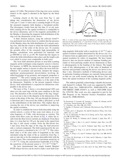
106103-3 Notes Rev. Sci. Instrum. 78, 106103 2007FIG. 4. A series <strong>of</strong> line scans taken for different I ac through the ring. Thedata have been multiplied by 1, 5, and 30 for 15 mA, 1.5 mA, and 150 A,respectively. The cross section <strong>of</strong> the wires <strong>of</strong> the ring is shown to denotethe wire position, but is not to scale.quency <strong>of</strong> 5 kHz. The position <strong>of</strong> the ring wire cross sectionsrelative to the signal is denoted in the figure by the blackcircles.Looking closely at the line scan from Fig. 3, andtaking into consideration the dimensions <strong>of</strong> our device146 m2 mm4 mm and a <strong>scanning</strong> height <strong>of</strong> 50 m,the measured magnetic field displays a broadened pr<strong>of</strong>ile.The discrepancy results from the fact that 1 in any nearfield<strong>scanning</strong> device the spatial resolution is comparable tothe device dimension, and 2 the magnetic permeability <strong>of</strong>the Metglas is distorting the magnetic field distribution <strong>of</strong> thering over the dimensions <strong>of</strong> the device.A finite element analysis, using the s<strong>of</strong>tware FEMM,was performed not shown here to confirm that the presence<strong>of</strong> the Metglas alters the field distribution <strong>of</strong> a current carryingwire, and that the extent to which the field redistributiontakes place is <strong>of</strong> the order <strong>of</strong> the device size. To examinethe possible effect <strong>of</strong> the extremely high permeability <strong>of</strong>Metglas, calculations were performed for materials with=400 000 as well as =40. We found that the degree towhich the field redistribution takes place and the length scaleover which it occurs were comparable in both cases.The local field distortion present in near-field <strong>scanning</strong>magnetic <strong>probe</strong> techniques using magnetic sensors is known.For instance, in MFM, the interaction between the magnetictip and sample surface is known to affect the local field distribution.To accurately and precisely interpret the images,significant postmeasurement deconvolution involving detailedknowledge <strong>of</strong> tip geometry and magnetic properties isrequired. 13,14 The active sensing area that needs to be modeledfor deconvolution in MFM studies is <strong>of</strong> the order <strong>of</strong> thetip dimensions. Similarly, in the present magnetic trilayerdevice, field redistribution is expected for dimensions comparableto the device size.The inset <strong>of</strong> Fig. 3 shows a two-dimensional 2D scantaken over the same ring with the same condition as the linescan. The distortion <strong>of</strong> the overall shape <strong>of</strong> the ring “image”to an oval one is due to the disparity in the dimensions <strong>of</strong> thesensor in the plane <strong>of</strong> the ring, 146 m through the thicknessx direction and 2 mm across the width y direction, as wellas the redistribution <strong>of</strong> the field lines. This implies that decreasingthe size <strong>of</strong> the device can contribute to improvingthe spatial resolution.In order to establish the lowest field detectable using thecurrent sensors, a series <strong>of</strong> line scans were taken, at a constantfrequency <strong>of</strong> 5 kHz, with decreasing ac currents. Theresults from these scans are shown in Fig. 4, where the resultsfrom the three lowest currents are displayed. From thesedata, it is clear that for 150 A, the peak in the signal fromthe ring is still clearly evident. From the Bio-Savart law,1 mm away from the edge <strong>of</strong> the ring, the field possessesonly a vertical component. The field experienced by the sensorat this point is calculated to be 1.510 −10 T. This calculatedvalue is <strong>of</strong> the same order <strong>of</strong> magnitude as the valuecalculated using the slope <strong>of</strong> the ac sensitivity from Fig. 1,and we take this to be the minimum detectable field with thecurrent sensor. This corresponds to a maximum sensitivity <strong>of</strong>310 −10 T. Using the measurement bandwidth <strong>of</strong> 0.33 Hz,the sensitivity <strong>of</strong> the present sensor is 510 −10 T/Hz 1/2 .We have demonstrated that simple bonded Metglas/PVDF trilayer devices can be used to make a near-field <strong>scanning</strong>magnetic field <strong>probe</strong> with a sensitivity <strong>of</strong> 10 −10 T and aspatial resolution roughly determined by the device size. It is<strong>of</strong> interest from an application’s point <strong>of</strong> view to increase thespatial resolution by orders <strong>of</strong> magnitude. We have found,however, that our present method <strong>of</strong> laminate bonding precludesus from pursuing smaller device dimensions as thereis inhomogeneity in the bonding <strong>of</strong> the trilayer. The lengthscale <strong>of</strong> this inhomogeniety is <strong>of</strong> the order <strong>of</strong> hundreds <strong>of</strong>microns and precludes reducing the device size down to lessthan 1 mm. Alternative methods <strong>of</strong> fabricating devices and,in particular, bonding techniques are currently being pursuedso that we can work toward reducing the device size, andhence the spatial resolution <strong>of</strong> the <strong>scanning</strong> magnetic <strong>probe</strong>.The authors gratefully acknowledge valuable discussionswith Samuel E. L<strong>of</strong>land. This work was supported by ONR-MURI Grant Nos. N000140110761, N000140610530, andNSF-MRSEC DMR 0520471 as well as NSF-DMR GrantNo. 0354740. This work was also supported in part by theIMI Program <strong>of</strong> the National Science Foundation underAward No. DMR-0603644.1 H. Kuramochi, T. Uzumaki, M. Yasutake, A. Tanaka, H. Akinage, and H.Yokoyama, Nanotechnology 16, 242005.2 S. J. Bending, Adv. Phys. 48, 449 1999.3 A. Sandhu, A. Okamoto, and I. Shibasaki, Microelectron. Eng. 73–74, 5242004.4 J. Clarke and A. I. Braginski, The SQUID Handbook Wiley, New York,2006, Vol. 2, p. 408.5 X. Liu, D. Mazumdar, W. Shen, B. D. Schrag, and G. Xiao, Appl. Phys.Lett. 89, 023504 2006.6 S. Stein, M. Wuttig, D. Viehland, and E. Quandt, J. Appl. Phys. 97, 12005.7 S. Dong, J. Zhai, J. Bai, J. Li, and D. Viehland, Appl. Phys. Lett. 87,062502 2005.8 S. Dong, J. Cheng, J. Li, and D. Viehland, Appl. Phys. Lett. 83, 48122003.9 J. Zhai, S. Dong, Z. Xing, J. Li, and D. Viehland, Appl. Phys. Lett. 89,083507 2006.10 Z. Xing, S. Dong, J. Li, and D. Viehland, Appl. Phys. Lett. 88, 0625102006.11 J. P. Teter, M. Wun-Fogle, A. E. Clark, and K. Mahoney, J. Appl. Phys.67, 5004 1990.12 R. M. Bozorth, Ferromagnetism Wiley, New York, 1993, p.845.13 M. R. Sheinfein, J. Unguris, D. T. Pierce, and R. J. Celotta, J. Appl. Phys.67, 5932 1990.14 T. Chang, M. Lagerquist, J.-G. Zhu, and J. H. Judy, IEEE Trans. Magn.28, 3138 1992.Downloaded 04 Oct 2007 to 129.2.175.79. Redistribution subject to AIP license or copyright, see http://rsi.aip.org/rsi/copyright.jsp