Dual JK flip-flop with reset; negative-edge trigger
Dual JK flip-flop with reset; negative-edge trigger
Dual JK flip-flop with reset; negative-edge trigger

Create successful ePaper yourself
Turn your PDF publications into a flip-book with our unique Google optimized e-Paper software.
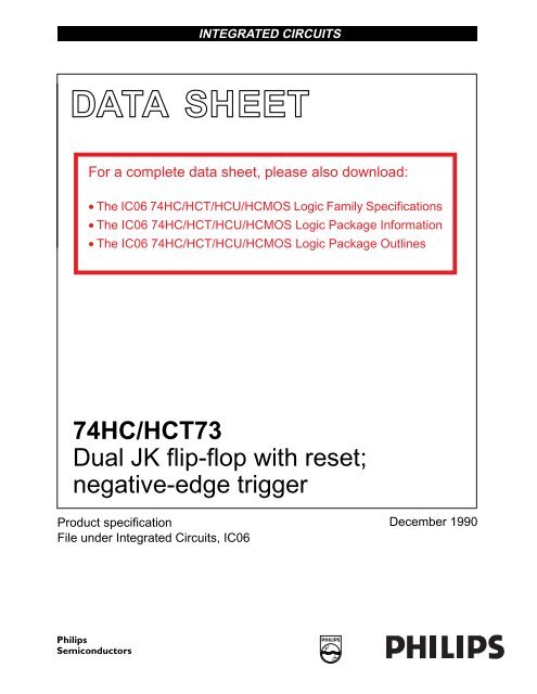
INTEGRATED CIRCUITSDATA SHEETFor a complete data sheet, please also download:• The IC06 74HC/HCT/HCU/HCMOS Logic Family Specifications• The IC06 74HC/HCT/HCU/HCMOS Logic Package Information• The IC06 74HC/HCT/HCU/HCMOS Logic Package Outlines74HC/HCT73<strong>Dual</strong> <strong>JK</strong> <strong>flip</strong>-<strong>flop</strong> <strong>with</strong> <strong>reset</strong>;<strong>negative</strong>-<strong>edge</strong> <strong>trigger</strong>Product specificationFile under Integrated Circuits, IC06December 1990
Philips SemiconductorsProduct specification<strong>Dual</strong> <strong>JK</strong> <strong>flip</strong>-<strong>flop</strong> <strong>with</strong> <strong>reset</strong>; <strong>negative</strong>-<strong>edge</strong> <strong>trigger</strong>74HC/HCT73FEATURES• Output capability: standard• I CC category: <strong>flip</strong>-<strong>flop</strong>sGENERAL DESCRIPTIONThe 74HC/HCT73 are high-speed Si-gate CMOS devicesand are pin compatible <strong>with</strong> low power Schottky TTL(LSTTL). They are specified in compliance <strong>with</strong> JEDECstandard no. 7A.The 74HC/HCT73 are dual <strong>negative</strong>-<strong>edge</strong> <strong>trigger</strong>ed<strong>JK</strong>-type <strong>flip</strong>-<strong>flop</strong>s featuring individual J, K, clock (nCP) and<strong>reset</strong> (nR) inputs; also complementary Q and Q outputs.The J and K inputs must be stable one set-up time prior tothe HIGH-to-LOW clock transition for predictableoperation.The <strong>reset</strong> (nR) is an asynchronous active LOW input.When LOW, it overrides the clock and data inputs, forcingthe Q output LOW and the Q output HIGH.Schmitt-<strong>trigger</strong> action in the clock input makes the circuithighly tolerant to slower clock rise and fall times.QUICK REFERENCE DATAGND = 0 V; T amb =25°C; t r =t f = 6 nsTYPICALSYMBOL PARAMETER CONDITIONSHC HCTUNITt PHL / t PLH propagation delay C L = 15 pF; V CC =5 VnCP to nQ 16 15 nsnCP to nQ 16 18 nsnR to nQ, nQ 15 15 nsf max maximum clock frequency 77 79 MHzC I input capacitance 3.5 3.5 pFC PD power dissipation capacitance per <strong>flip</strong>-<strong>flop</strong> notes 1 and 2 30 30 pFNotes1. C PD is used to determine the dynamic power dissipation (P D in µW):P D =C PD × V 2 CC × f i +∑(C L × V 2 CC × f o ) where:f i = input frequency in MHzf o = output frequency in MHz∑ (C L × V 2 CC × f o ) = sum of outputsC L = output load capacitance in pFV CC = supply voltage in V2. For HC the condition is V I = GND to V CCFor HCT the condition is V I = GND to V CC − 1.5 VORDERING INFORMATIONSee “74HC/HCT/HCU/HCMOS Logic Package Information”.December 1990 2
Philips SemiconductorsProduct specification<strong>Dual</strong> <strong>JK</strong> <strong>flip</strong>-<strong>flop</strong> <strong>with</strong> <strong>reset</strong>; <strong>negative</strong>-<strong>edge</strong> <strong>trigger</strong>74HC/HCT73PIN DESCRIPTIONPIN NO. SYMBOL NAME AND FUNCTION1, 5 1CP, 2CP clock input (HIGH-to-LOW, <strong>edge</strong>-<strong>trigger</strong>ed)2, 6 1R, 2R asynchronous <strong>reset</strong> inputs (active LOW)4 V CC positive supply voltage11 GND ground (0 V)12, 9 1Q, 2Q true <strong>flip</strong>-<strong>flop</strong> outputs13, 8 1Q, 2Q complement <strong>flip</strong>-<strong>flop</strong> outputs14, 7, 3, 10 1J, 2J, 1K, 2K synchronous inputs; <strong>flip</strong>-<strong>flop</strong>s 1 and 2Fig.1 Pin configuration. Fig.2 Logic symbol. Fig.3 IEC logic symbol.December 1990 3
Philips SemiconductorsProduct specification<strong>Dual</strong> <strong>JK</strong> <strong>flip</strong>-<strong>flop</strong> <strong>with</strong> <strong>reset</strong>; <strong>negative</strong>-<strong>edge</strong> <strong>trigger</strong>74HC/HCT73FUNCTION TABLEOPERATINGINPUTSOUTPUTSMODEnR nCP J K Q Qasynchronous <strong>reset</strong> L X X X L Htoggleload “0” (<strong>reset</strong>)load “1” (set)hold “no change”HHHH↓↓↓↓hlhlhhllqLHqqHLqNotes1. H = HIGH voltage levelh = HIGH voltage level one set-up time prior to the HIGH-to-LOW CPtransitionL = LOW voltage levelI = LOW voltage level one set-up time prior to the HIGH-to-LOW CPtransitionq = lower case letters indicate the state of the referenced output oneset-up time prior to the HIGH-to-LOW CP transitionX = don’t care↓ = HIGH-to-LOW CP transitionFig.4 Functional diagram.Fig.5 Logic diagram (one <strong>flip</strong>-<strong>flop</strong>).December 1990 4
Philips SemiconductorsProduct specification<strong>Dual</strong> <strong>JK</strong> <strong>flip</strong>-<strong>flop</strong> <strong>with</strong> <strong>reset</strong>; <strong>negative</strong>-<strong>edge</strong> <strong>trigger</strong>74HC/HCT73DC CHARACTERISTICS FOR 74HCFor the DC characteristics see “74HC/HCT/HCU/HCMOS Logic Family Specifications”.Output capability: standardI CC category: <strong>flip</strong>-<strong>flop</strong>sAC CHARACTERISTICS FOR 74HCGND = 0 V; t r =t f = 6 ns; C L = 50 pFSYMBOLt PHL / t PLHt PHL / t PLHt PHL / t PLHPARAMETERpropagation delaynCP to nQpropagation delaynCP to nQpropagation delaynR to nQ, nQT amb (°C)74HC+25 −40 to +85 −40 to +125min. typ. max. min. max. min. max.521915521915501814t THL / t TLH output transition time 1976t Wt Wt remt sut hf maxclock pulse widthHIGH or LOW<strong>reset</strong> pulse widthHIGH or LOWremoval timenR to nCPset-up timenJ, nK to nCPhold timenJ, nK to nCPmaximum clock pulsefrequency8016148016148016148016143336.030352286228622862286−8−3−223708316032271603227145292575151310020171002017100201710020173334.8242820040342004034180363195191612024201202420120242012024203334.020242404841240484122044381102219UNITTEST CONDITIONSV CC(V)ns 2.04.56.0ns 2.04.56.0ns 2.04.56.0ns 2.04.56.0ns 2.04.56.0ns 2.04.56.0ns 2.04.56.0ns 2.04.56.0ns 2.04.56.0MHz 2.04.56.0WAVEFORMSFig.6Fig.6Fig.7Fig.6Fig.6Fig.7Fig.7Fig.6Fig.6Fig.6December 1990 5
Philips SemiconductorsProduct specification<strong>Dual</strong> <strong>JK</strong> <strong>flip</strong>-<strong>flop</strong> <strong>with</strong> <strong>reset</strong>; <strong>negative</strong>-<strong>edge</strong> <strong>trigger</strong>74HC/HCT73DC CHARACTERISTICS FOR 74HCTFor the DC characteristics see “74HC/HCT/HCU/HCMOS Logic Family Specifications”.Output capability: standardI CC category: <strong>flip</strong>-<strong>flop</strong>sNote to HCT typesThe value of additional quiescent supply current (∆I CC ) for a unit load of 1 is given in the family specifications.To determine ∆I CC per input, multiply this value by the unit load coefficient shown in the table below.INPUTnKnRnCP, nJUNIT LOAD COEFFICIENT0.600.651.00AC CHARACTERISTICS FOR 74HCTGND = 0 V; t r =t f = 6 ns; C L = 50 pFSYMBOLPARAMETERT amb (°C)74 HCT+25 −40 to +85 −40 to +125UNITTEST CONDITIONSmin. typ. max. min. max. min. max.t PHL / t PLH propagation delay18 38 48 57 ns 4.5 Fig.6nCP to nQt PHL / t PLH propagation delay21 36 45 54 ns 4.5 Fig.6nCP to nQt PHL / t PLH propagation delay20 34 43 51 ns 4.5 Fig.7nR to nQ, nQt THL / t TLH output transition time 7 15 19 22 ns 4.5 Fig.6VCC(V)WAVEFORMSt Wt Wt remt sut hf maxclock pulse widthHIGH or LOW<strong>reset</strong> pulse widthHIGH or LOWremoval timenR to nCPset-up timenJ, nK to nCPhold timenJ, nK to nCPmaximum clock pulsefrequency16 8 20 24 ns 4.5 Fig.618 9 23 27 ns 4.5 Fig.714 8 18 21 ns 4.5 Fig.712 6 15 18 ns 4.5 Fig.63 −2 3 3 ns 4.5 Fig.630 72 24 20 MHz 4.5 Fig.6December 1990 6
Philips SemiconductorsProduct specification<strong>Dual</strong> <strong>JK</strong> <strong>flip</strong>-<strong>flop</strong> <strong>with</strong> <strong>reset</strong>; <strong>negative</strong>-<strong>edge</strong> <strong>trigger</strong>74HC/HCT73AC WAVEFORMSThe shaded areas indicate when the input ispermitted to change for predictable outputperformance.(1) HC : V M = 50%; V I = GND to V CC .HCT: V M = 1.3 V; V I = GND to 3 V.Fig.6Waveforms showing the clock (nCP) to output (nQ, nQ) propagation delays, the clock pulse width, the Jand K to nCP set-up and hold times, the output transition times and the maximum clock pulse frequency.(1) HC : V M = 50%; V I = GND to V CC .HCT: V M = 1.3 V; V I = GND to 3 V.Fig.7Waveforms showing the <strong>reset</strong> (nR) input to output (nQ, nQ) propagation delays and the <strong>reset</strong> pulse widthand the nR to nCP removal time.PACKAGE OUTLINESSee “74HC/HCT/HCU/HCMOS Logic Package Outlines”.December 1990 7