LNâ3 IDLE MIND SOLUTIONS 1. Let us first look in most general ...
LNâ3 IDLE MIND SOLUTIONS 1. Let us first look in most general ...
LNâ3 IDLE MIND SOLUTIONS 1. Let us first look in most general ...

Create successful ePaper yourself
Turn your PDF publications into a flip-book with our unique Google optimized e-Paper software.
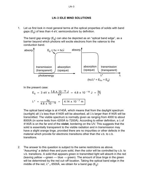
LN–3LN–3 <strong>IDLE</strong> <strong>MIND</strong> <strong>SOLUTIONS</strong><strong>1.</strong> <strong>Let</strong> <strong>us</strong> <strong>first</strong> <strong>look</strong> <strong>in</strong> <strong>most</strong> <strong>general</strong> terms at the optical properties of solids with bandgaps (E g ) of less than 4 eV, semiconductors by def<strong>in</strong>ition.The band gap energy (E g ) can also be depicted as an “optical band edge”, as abarrier beyond which photons will excite electrons from the valence to theconduction band.absorp.E g = hν = hcνabsorp.transmission(transparent)absorption(opaque)absorption(opaque)transmission(transparent)photoenergyλ* λ(hc/λ* = E hν = E g )In the present case:E g + 3eVx <strong>1.</strong>6 x 10*19 J + 4.8 x 10*19J + hceV l *l * + hc + 4.14 x 10 *7 m4.8 x 10 *19The optical band edge is at 4140Å, which means that from the daylight spectrum(sunlight) all λ’s less than 4140Å will be absorbed, all λ’s larger than 4140Å will betransmitted. The visible spectrum is normally given as rang<strong>in</strong>g from 4000 to about8000Å (<strong>in</strong> some texts from 4200Å to 7200Å). Accord<strong>in</strong>g to either def<strong>in</strong>ition, a λ of4140Å is on the far end of the violet, border<strong>in</strong>g on the UV. This suggests that thesolid is essentially transparent to the visible radiation and <strong>in</strong> transmission mayhave a slight orange t<strong>in</strong>ge, provided there are no impurities or other defects <strong>in</strong> thematerial which provide for electronic transitions other than the v.b. to c.b.transitions.2. The answer to this question is subject to the same restrictions as above.“Assum<strong>in</strong>g” a defect–free and pure solid, then the color will be controlled by c.b. tov.b. transitions. A solid that appears green <strong>in</strong> transmitted light will absorb <strong>in</strong> the red(leav<strong>in</strong>g yellow ––green –– blue → green). The amount of blue t<strong>in</strong>ge <strong>in</strong> the greenwill be determ<strong>in</strong>ed by the red cut–off location. Tak<strong>in</strong>g the optical band edge <strong>in</strong> themiddle of the red, λ* ± 6500Å, we obta<strong>in</strong> for a band gap (E g ):
LN–32. Cont<strong>in</strong>ued.E g + E hn+ hc +l *6.63 x 10 *34 x3x10 86.5 x 10 *7+ 3.06 x 10 *19 Jx 1eV + <strong>1.</strong>9 eV<strong>1.</strong>6 x 10 *19 J3. Both compounds are of the III–V family, which hybridize and form “adamant<strong>in</strong>e”(diamond–like) structures which places them <strong>in</strong>to the category of semiconductor.AlNGaSbΔEN = <strong>1.</strong>43. The covalent radii of the constituents are small and,comb<strong>in</strong>ed with the large ΔEN, the bonds (polar covalencies) are verystrong – the semiconductor is expected to exhibit a large band gap(likely transparent).ΔEN = 0.24. The covalent radii of both constituents are significantly larger(than those of AlN), the ionic contribution to bond<strong>in</strong>g is small – thesemiconductor is expected to exhibit a much smaller band gap thanAlN.(AlN, E g = 3.8 eV,GaSb, E g = 0.8 eV)4. (a) Na 3s valence band is half–filled. EElectrons may acquire additional<strong>in</strong>cremental energy and moveabout (conduct).filledΔE(b) Mg 3s valence band is completely filled;however, the 3p band, which isempty, partly overlaps the filledvalence band and provides forelectrical conductivity.filledemptyΔE3s}}3p
LN–35. Consider<strong>in</strong>g electronic transitions only, the answer <strong>in</strong> pr<strong>in</strong>ciple is the same for allthree materials: there is no limit. But rephrased (λ = hc/E) – which is the lowestenergy radiation still capable of be<strong>in</strong>g transmitted through a material? – thequestion makes sense; we are concerned about a cut–off wavelength beyondwhich the radiation is be<strong>in</strong>g absorbed. Absorption means the energy is be<strong>in</strong>gtransferred to an electron. Such a transfer can only take place if E (photon) ≥ ΔE.The critical energy (E = hν = hc/λ) is presently given by the value of the energygap (E g ).(a) Si: E g = <strong>1.</strong>1eV = <strong>1.</strong>1 x <strong>1.</strong>6 x 10 –19 J = <strong>1.</strong>76 x 10 –19 J = hc/λl crit+hc<strong>1.</strong>76 x 10 *19 + <strong>1.</strong>13 x 10 *6 m + <strong>1.</strong>13 mm(b) Ge: E g = 0.7eV = <strong>1.</strong>12 x 10 –19 Jl crit+ <strong>1.</strong>77 x 10 *6 m + <strong>1.</strong>8 mm(c) GaAs: E g = <strong>1.</strong>43eV = 2.29 x 10 –19 Jl crit+ 0.87 x 10 *6 m + 0.87 mm6. An extr<strong>in</strong>sic semiconductor is a semiconductor which conta<strong>in</strong>s foreign elementscapable of contribut<strong>in</strong>g mobile charge carriers, electrons, to the conduction band(n–type) or holes to the valence band (p–type). An <strong>in</strong>tr<strong>in</strong>sic semiconductorconta<strong>in</strong>s no foreign elements.7. The question is answered by determ<strong>in</strong><strong>in</strong>g (a) the volume of 50g Si and (b) thenumber of P atoms <strong>in</strong> 3 mg = 3x10 –3 g P.r Si + 2.33 gcm 3 50 g;+ 2<strong>1.</strong>46 cm 32.33 gcm 330.97 g P + 6.02 x 10 23 atoms atomic weight of P = 30.79 g3mg + 3x10 *3 g + 6.02 x 1023 x3x10 *3 + 5.83 x 10 19 atoms30.97Number P atomscm 3 silicon + 5.83 x 10¹⁹ + 2.7 x 10 18 cm 32<strong>1.</strong>46
LN–38.E••••E diagram for K}3d band empty4s band half filleddist.E•••E diagram for Be}dist.2s filled}2p overlapp<strong>in</strong>gIn K, each atom contributes one electron and one orbital to the conduction band(4s band). Accord<strong>in</strong>g to the Pauli excl<strong>us</strong>ion pr<strong>in</strong>ciple, each “molecular orbital”formed <strong>in</strong> the band (energy state) can accommodate two electrons. As aconsequence, the conduction band is only half–filled with electrons – whichprovides for electrical conduction.In Be, each atom contributes two electrons and one orbital to the conduction band(2s band). With two electrons per orbital (from each atom) the 2s conduction bandis filled. The observed electrical conductivity is due to the overlapp<strong>in</strong>g 2p band,which is empty and th<strong>us</strong> provides empty energy states required for electronicconduction.9. (a) E g = 3.2eV = 3.2 x <strong>1.</strong>6 x 10 –19 J = 5.12 x 10 –19 JThe full band gap (energy) corresponds to 5.12 x 10 –19 J. If we <strong>look</strong> for thecorrespond<strong>in</strong>g wavelength of radiation, we have:E + hn + hc and l + hc + 6.6 x 10 *34 x3x10 8l E 5.12 x 10 *19l + 3.879 x 10 *7 m +3880ÅThe visible spectrum ranges from 4000–7500Å. S<strong>in</strong>ce only radiation withE ≥ E g will be absorbed (λ < 3880Å), the material is transparent to visiblelight.
LN–39. (b) Most oxide semiconductors are either doped to create extr<strong>in</strong>sic defects orare annealed under conditions <strong>in</strong> which they become nonstoichiometric.When ZnO becomes nonstoichiometric, it is commonly beca<strong>us</strong>e of an excessmetal content, for example, Zn 1+x O. This Zn 1+x O is a negative carrier(n–type) oxide conductor and is sometimes called an “excess”semiconductor.10. (a) [T <strong>in</strong> thermally activated processes is the absolute temperature –T o K = (273.16 + t o C); Boltzmann’s constant = k = <strong>1.</strong>38 x 10 –23 J/ o K]T = 293.16K:n i+ 9.7 x 10 15 x 293.16 32 xe * 0.72x<strong>1.</strong>6x10 *192x<strong>1.</strong>38x10 *23 x 293.16+ 9.7 x 10 15 x 5019 x 6.6 x 10 *7n i+ 3.21 x 10 13 cm 3(b) 200 o C = 473.16Kn i+ 9.7 x 10 15 x 473.16 2xe0.72x<strong>1.</strong>6x10**193 2x<strong>1.</strong>38x10 *23 x 473.16n i(200K) + 9.7 x 10 15 x <strong>1.</strong>03 x 10 4 x <strong>1.</strong>47 x 10 *4n i+ <strong>1.</strong>47 x 10 16 cm 3The number of conduct<strong>in</strong>g electrons (<strong>in</strong> the conduction band) at 200 o C is byabout five orders of magnitude less than that of a good conductor. Thematerial will not be a good conductor. (There are additional factors whichcontribute to the “relatively poor conductivity” of Ge at this temperature.)1<strong>1.</strong> E th+ 3kT E g + 0.72 x <strong>1.</strong>6 x 10 *19 J2T + 0.72 x <strong>1.</strong>6 x 10*19 x2 + 5565K +3 x <strong>1.</strong>38 x 10 *235.3 x 10 3o CThe temperature would have to be 5.3 x 10 3 o C (about 4400 o C above the melt<strong>in</strong>gpo<strong>in</strong>t).12. (a) From our limited knowledge of the conduction behavior, we m<strong>us</strong>t assumethat <strong>in</strong> semiconductors the conductivity will <strong>in</strong>crease with T s<strong>in</strong>ce the numberof electrons <strong>in</strong> the conduction band <strong>in</strong>creases.
LN–312. (b) As a <strong>first</strong> approximation, we can say that the number of free electrons is<strong>in</strong>dependent of T; that, however, the atoms <strong>in</strong> the lattice will, with <strong>in</strong>creas<strong>in</strong>gtemperature, be subject to <strong>in</strong>creased oscillations about their (relatively) fixedposition. These oscillations provide greater opportunity for “scatter<strong>in</strong>g” ofconduct<strong>in</strong>g electrons and th<strong>us</strong> will “reduce” the mobility of the electrons. Wecan expect the electrical conductivity of metals to decrease with <strong>in</strong>creas<strong>in</strong>gtemperature.13. (a) The optical properties of ZnSe can be expla<strong>in</strong>ed when compar<strong>in</strong>g the“energy band” of the visible spectrum with the energy band diagram of ZnSe.E(hν)E–c.b.E g = 2.3eVabsorption takes place(photo–excitation) forall radiation withE (hν) ≥ 2.3 eV.+v.b.λ(Å) →40005397↓7000blue–greenyellow–red3.1↑2.32.26 <strong>1.</strong>77← E(eV)
LN–313. (a) Cont<strong>in</strong>ued.absorp.<strong>1.</strong>0blue–greenabsorbedyellow–redtransmitted0.05397λ(Å) wavelengthFrom the energy distribution of the visible spectrum we recognize that theblue–green portion has photon energies <strong>in</strong> excess of the band gap(E g = 2.3eV) and th<strong>us</strong> will be absorbed. The yellow–red potion, on the otherhand, has photon energies less than the band gap – it will be transmitted.ZnSe, therefore, is expected to exhibit a yellowish–red color.(b)In pr<strong>in</strong>ciple there are two ways to <strong>in</strong>crease the electrical conductivity ofZnSe:(1) A temperature rise. Any rise <strong>in</strong> temperature will <strong>in</strong>crease the numberof “thermally activated” charge carriers <strong>in</strong> the conduction band(electrons) and <strong>in</strong> the valence band (holes) and, th<strong>us</strong>, the electronicconductivity.[The electrical conductivity of solids, demonstrated by the flow ofelectronic charge carriers under an applied electric field (E), can beformulated through Ohm’s law, J = σE, which states that the currentdensity (J = number of charges transported through a unit area <strong>in</strong> aunit time) is proportional (σ = conductivity) to the applied electric field.Accord<strong>in</strong>gly:J = N e v dwhere N = number of charge carriers/unit volume, e = electroniccharge and v d = average drift velocity of charge carriers <strong>in</strong> an appliedelectric field. We th<strong>us</strong> obta<strong>in</strong>:σ = (N e v d )/E
LN–313. (b) Cont<strong>in</strong>ued.(1) cont<strong>in</strong>ued –and if we def<strong>in</strong>e (v d /E) = µ, the charge carrier mobility, we have:σ = N e µIn <strong>in</strong>tr<strong>in</strong>sic semiconductors we have both electrons and holescontribut<strong>in</strong>g to conduction:σ = N e eµ e + N n eµ h = Ne(µ e + µ h )s<strong>in</strong>ce N e = N h . Tak<strong>in</strong>g the number of thermally generated chargecarriers, the relationshipN + AT 32 exp *E g 2kTwe obta<strong>in</strong> the temperature dependence of the conductivity as:s + AT 32 exp *E g2kTxe(m e ) m h)To assess the temperature dependence of electrical conductivity wem<strong>us</strong>t take <strong>in</strong>to consideration that, beca<strong>us</strong>e of <strong>in</strong>creased vibration ofthe atoms about their lattice positions, the charge carrier mobility willdecrease (<strong>in</strong>creased scatter<strong>in</strong>g of charge carriers) with <strong>in</strong>creas<strong>in</strong>gtemperature. This effect expla<strong>in</strong>s why the electronic conductivity <strong>in</strong>metals, where N is constant, will decrease with <strong>in</strong>creas<strong>in</strong>gtemperature. In semiconductors, where N <strong>in</strong>creases with temperature,the accompany<strong>in</strong>g mobility effect is not apparent at low temperatures(conductivity <strong>in</strong>creases), but becomes pronounced at hightemperatures (conductivity decreases).](2) Introduction of shallow impurity (or defect) states close to theconduction or valence band. This is accomplished by the<strong>in</strong>corporation of appropriate dopant elements <strong>in</strong>to the crystal matrix. Ifthese impurities are shallow ( ~ 0.01eV from the conduction or valenceband), they will be totally ionized at room temperature and each willcontribute an electron (donor dopant: K, Na) or holes (acceptordopant: G, Br), th<strong>us</strong> <strong>in</strong>creas<strong>in</strong>g the electrical conductivity without thenecessity of a temperature rise. (Be aware that certa<strong>in</strong> defects <strong>in</strong> thecrystal lattice may also <strong>in</strong>crease the electronic conductivity.)
LN–314. (a) This crystal is extr<strong>in</strong>sic of p–type conductivity – i.e. holes <strong>in</strong> the valence band(majority charge carriers) are primarily responsible for electronic conduction.p–type conductivity results from the fact that the substitutional dop<strong>in</strong>gelement, boron, has only three valence electrons. Upon <strong>in</strong>corporation, boronhas a tendency to attract an additional electron from the matrix (valenceband) to satisfy the bond<strong>in</strong>g requirements (formation of four covalent bonds).In do<strong>in</strong>g so, each boron atom assumes a negative charge (which is notmobile) and simultaneo<strong>us</strong>ly creates a mobile hole.(b)Approach: determ<strong>in</strong>e the number of atoms <strong>in</strong> 28 mg boron and the volume of100 g silicon.ρ Si= 2.33 g/cm 3At.Wt. B= 10.81 g/moleVolume of 100 g Si = (100/2.33) = 42.9 cm 3# atoms per 28mg B+6.02 x 10 23 x28x10 *3 +10.81<strong>1.</strong>56 x 10 21When <strong>in</strong>corporated uniformly <strong>in</strong>to a volume of 42.9 cm 3 of silicon, thenumber of boron atoms per cm 3 (the number of extr<strong>in</strong>sic charge carriers –i.e. the number of holes generated) is:<strong>1.</strong>56 x 10 21 + 3.6 x 10 1942.9[It should be specified that this number applies to silicon at roomtemperature. Assume the temperature were approach<strong>in</strong>g 0 K; then thenumber of extr<strong>in</strong>sic charge carriers would approach “zero” s<strong>in</strong>ce the impuritylevels are, by a f<strong>in</strong>ite amount (~0.01 eV), above the top of the valence bandand the acquired charges will drop back to the lowest possible energy state.]EB E– – – –+ + + +T→ o KvalencebandBvalenceband
LN–315. “White light” conta<strong>in</strong>s radiation <strong>in</strong> wavelength rang<strong>in</strong>g from about 4000Å (violet) to7000Å (deep red). A material appear<strong>in</strong>g red <strong>in</strong> transmission has the follow<strong>in</strong>gabsorption characteristics:absorp.blue–yellowabsorbed4000 6500redtransmittedλ (Å)(a)(b)If the material is pure (no impurity states present), then it m<strong>us</strong>t be classifiedas a semiconductor s<strong>in</strong>ce it exhibits a f<strong>in</strong>ite “band gap” – i.e. to activatecharge carriers, photons with energies <strong>in</strong> excess of “red” radiation arerequired.Tak<strong>in</strong>g λ = 6500Å as the optical absorption edge for this material, we have:E hn+ hcl+ 3.05 x 10 *29 Jx 1eV<strong>1.</strong>6 x 10 *19 J+ <strong>1.</strong>9 eVAccord<strong>in</strong>gly, the band gap for the material is E g = <strong>1.</strong>9 eV.16. (a) The antimony–doped Ge is n–type beca<strong>us</strong>e Sb (with electronic configuration[Kr]4d 10 5s 2 5p 3 ) has five valence electrons, and, therefore, donates one tothe Ge ([Ar]3d 10 4s 2 4p 2 ).(b)Assume uniform dop<strong>in</strong>g of Ge with Sb. Each Sb atom contributes oneelectron to germanium’s conduction band.27 mg +2.7(10 *2 )g12<strong>1.</strong>75 gmole + 2.2(10*4 )moleSbSo the antimony addition contributes2.2(10 –4 ) x 6.02(10 23 ) = <strong>1.</strong>32(10 20 ) electrons
LN–316. (b) Cont<strong>in</strong>ued.The volume of germanium is:110 g+ 20.7 cm 35.32 gcm 3n e + <strong>1.</strong>32(1020 ) + 6.4(10 18 *3)cm20.7 cm 317. Need to f<strong>in</strong>d E g :ν = 5.631 x 10 5 m –1λ = 1/ν = <strong>1.</strong>776 x 10 –6 mE g = (hc)/λ = (hc)ν = 0.698 eV[Looks like Ge.]T = 250 o C = 523Kn i+ AT 32 e *E g 2kTcm *30.698+ (5 x 10 15 ) (523) 32 exp* 2 x (8.63 x 10 *5 ) (523)= [5 x 10 15 ] [<strong>1.</strong>196 x 10 4 ] exp [–7.688]= 2.74 x 10 16 cm –318. (a) From the lecture notes you know that a group III element, substitutionally<strong>in</strong>corporated <strong>in</strong>to silicon, acts as an “acceptor” dopant, and by acquir<strong>in</strong>gelectrons from the lattice (valence band) will generate “positive holes” – thecrystal will have an excess of (positive) holes – and it will be p–type.
LN–318. (b) First we determ<strong>in</strong>e the volume of 100g Si, then the number of Al atoms per33 mg Al and divide this number by the volume of silicon. This gives <strong>us</strong> thenumber of Al atoms per cm 3 Si – which is the same as the number ofextr<strong>in</strong>sic charge carriers, s<strong>in</strong>ce each Al generates one carrier.Vol. Si +100 g2.33 gcm 3+ 42.9 cm 3 100 g33 mg Al conta<strong>in</strong>:6.02 x 10 23 atoms x33x10 *3 g + 7.36 x 10 20 atoms26.98 g# Al atoms per cm 3 = # charge carriers per cm 3+ 7.36 x 10²⁰ + <strong>1.</strong>72 x 10 19 Alcm 3 Si42.9= <strong>1.</strong>72 x 10 19 extr<strong>in</strong>sic holes per cm 3 Si19. S<strong>in</strong>ce E = hν, we f<strong>in</strong>d the material to be transparent to photons with energies lessthan:(6.63 x 10 *34 Js) x (<strong>1.</strong>3 x 10 14 s *1 )x 1eV + 0.54 eV<strong>1.</strong>6 x 10 *19 Jwhich constitutes the absorption edge, ie the energy band gap.Econduction bandE g = 0.54 eVvalence band
LN–320. (An <strong>in</strong>advertent error occurred <strong>in</strong> the relationship for thermally activated chargecarriers. It should be:n e + AT 32 e *E g 2kTcm 3Also, the dimension of A should be [cm –3 x ( o K) –3/2 ].)This trivia question therefore has the answer:n e + 5x10 15 x (500 ) 273.15)2 xe3*<strong>1.</strong>1x<strong>1.</strong>6x10 *192x<strong>1.</strong>38x10 *23 x 773.15n e = 5 x 10 15 x 773.15 3/2 x e –8.25 cm –3n e = 2.8 x 10 16 cm –32<strong>1.</strong> (a)E5 x 10 18 extr<strong>in</strong>sic carriers (c.b.)– – – – – – –↑ ↑ ↑↑↑↑↑+ + + + + + + ←donor impurity levelE g = 0.7 eV(v.b.)(b)The band gap of E g = 0.7 eV x <strong>1.</strong>6 x 10 –19 J = <strong>1.</strong>1 x 10 –19 J corresponds to acut–off frequency (E g = hν):n +<strong>1.</strong>1 x 10*19+6.63 x 10 *34<strong>1.</strong>66 x 10 14 s*1The <strong>in</strong>dicated frequency (1 x 10 15 s –1 ) is higher – the photon energy is largerthan E g . The radiation will be absorbed by germanium and the crystal isopaque to this radiation.
LN–322.23. 6.63x10 *34 Js x 3x10 8 msE + hc ++ 6.63 x 10300m*38 photonJphotonlThe energy of the radio transmitter = Power x time= 50 x 10 3 J/s x 60s = 3 x 10 6 JNumber of photons =3x10 6 J= 4.52 x 10 33 photons6.63x10 *28 Jphoton24. (a) l + c + 3x10⁸ ms + 6x10 *7 m + 600nmn 5x10 14 s(b)The color will be orange or “reddish”.
LN–324. (c) The band gap energy E g = E photon = hν= 6.63x10 –34 Js x 5x10 14 /s= 3.315x10 –19 J x 1eV/<strong>1.</strong>6x10 –18 J= 2.07 eV25. (Determ<strong>in</strong>e the volume of 30g Ge – from that determ<strong>in</strong>e the mg of As/cm 3 andconvert that quantity <strong>in</strong>to # of As atoms (carriers)/cm 3 .)30gGe x 1cm3 + 5.64cm 3 ; 5.4x10 *2 gAs+ 9.57x10*3 gAs5.32g5.64cm 3 cm 39.57x10 *3 gAs x 6.02x1023 atoms = 7.69 x 10 19 carriers/cm 374.92g26.27. (a) 1 1 visiblel + + mrad.= 0.62µm100n <strong>1.</strong>613x10 6 0 0.4 0.6 0.7 λ [µm]Abs [%]bluered(b)The color will be reddish–orange.
![18.03 Class 21, April 3 Fun with Fourier series [1] If f(t) is any decent ...](https://img.yumpu.com/51148985/1/190x245/1803-class-21-april-3-fun-with-fourier-series-1-if-ft-is-any-decent-.jpg?quality=85)