CHAPTER 4: IMPERFECTIONS IN SOLIDS
CHAPTER 4: IMPERFECTIONS IN SOLIDS
CHAPTER 4: IMPERFECTIONS IN SOLIDS

Create successful ePaper yourself
Turn your PDF publications into a flip-book with our unique Google optimized e-Paper software.
5.1 Introduction• Every single solid has defects andimperfections.• Sometimes the imperfections are purposelycreated and used for a specific purpose.• Types of defects:– Point Defects (One or two atomic positions)– Linear Defects (One Dimensional)– Interfacial Defects (Boundaries)
5.1 Imperfections in Solids• Solidification- result of casting of molten material– 2 steps• Nuclei form• Nuclei grow to form crystals – grain structure• Start with a molten material – all liquidnucleiliquidcrystals growing grain structureAdapted from Fig. 5.19 (b), Callister & Rethwisch 3e.• Crystals grow until they meet each otherChapter 5 - 4
Polycrystalline MaterialsGrain Boundaries• regions between crystals• transition from lattice ofone region to that of theother• slightly disordered• low density in grainboundaries– high mobility– high diffusivity– high chemical reactivityAdapted from Fig. 5.12,Callister & Rethwisch 3e.Chapter 5 - 5
Grains can beSolidification- equiaxed (roughly same size in all directions)- columnar (elongated grains)~ 8 cmheatflowColumnar inarea with lessundercoolingAdapted from Fig. 5.17,Callister & Rethwisch 3e.Shell ofequiaxed grainsdue to rapidcooling (greater∆T) near wallGrain Refiner - added to make smaller, more uniform, equiaxed grains.Chapter 5 - 6
Imperfections in SolidsThere is no such thing as a perfect crystal.• What are these imperfections?• Why are they important?Many of the important properties ofmaterials are due to the presence ofimperfections.Chapter 5 - 7
Types of Imperfections• Vacancy atoms• Interstitial atoms• Substitutional atoms• Dislocations• Grain BoundariesPoint defectsLine defectsArea defectsChapter 5 - 8
I. PointdefectsChapter 5 - 9
5.2 Point Defects in Metals• Vacancies:-vacant atomic sites in a structure.distortionof planesVacancy• Self-Interstitials:-"extra" atoms positioned between atomic sites.distortionof planesselfinterstitialChapter 5 - 10
Equilibrium Concentration:Point Defects• Equilibrium concentration varies with temperature!No. of defectsNo. of potentialdefect sitesEach lattice siteis a potentialvacancy siteN v N = ⎛exp − Q ⎞⎜v÷⎝ kT ⎠Activation energyTemperatureBoltzmann's constant(1.38 x 10 -23 J/atom-K)(8.62 x 10 -5 eV/atom-K)Chapter 5 - 11
Measuring Activation Energy• We can get Q v froman experiment.• Measure this...N ⎛ v N = exp − Q ⎞⎜ v÷⎝ kT ⎠• Replot it...NvNexponentialdependence!NvlnNslope-Qv /kdefect concentrationT1/TChapter 5 - 12
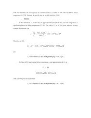
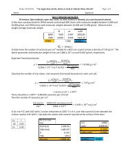
Estimating Vacancy Concentration• Find the equil. # of vacancies in 1 m 3 of Cu at 1000°C.• Given:ρ = 8.4 g/cm 3 A Cu = 63.5 g/molQ v = 0.9 eV/atom N A = 6.02 x 10 23 atoms/molFor 1 m 3 , N = ρ x• Answer:N AA Cu0.9 eV/atomN v ÷N = ⎛exp − Q ⎞⎜ v⎝ kT ⎠÷= 2.7 x 10 -41273 K8.62 x 10 -5 eV/atom-Kx 1 m 3 = 8.0 x 10 28 sitesNv = (2.7 x 10 -4 )(8.0 x 10 28 ) sites = 2.2 x 10 25 vacanciesChapter 5 - 13
5.2 Point Defects in Metals• Self Interstitial:– When an atom ispushed into aninterstitial site which isnormally unoccupied.– Very small amount inmetals because when itoccurs, it highly distortsthe metal.– Much lowerconcentrations thanvacancies.http://www.substech.com/dokuwiki/doku.php?id=imperfections_of_crystal_structure
5.3 Point Defects in Ceramics (i)• Vacancies-- vacancies exist in ceramics for both cations and anions• Interstitials-- interstitials exist for cations-- interstitials are not normally observed for anions because anionsare large relative to the interstitial sitesAnionVacancyCationInterstitialCationVacancyAdapted from Fig. 5.2, Callister &Rethwisch 3e. (Fig. 5.2 is fromW.G. Moffatt, G.W. Pearsall, andJ. Wulff, The Structure andProperties of Materials, Vol. 1,Structure, John Wiley and Sons,Inc., p. 78.)Chapter 5 - 16
Point Defects in Ceramics (ii)• Frenkel Defect-- a cation vacancy-cation interstitial pair.• Shottky Defect-- a paired set of cation and anion vacancies.ShottkyDefect:FrenkelDefectAdapted from Fig. 5.3, Callister &Rethwisch 3e. (Fig. 5.3 is fromW.G. Moffatt, G.W. Pearsall, andJ. Wulff, The Structure andProperties of Materials, Vol. 1,Structure, John Wiley and Sons,Inc., p. 78.)• Equilibrium concentration of defects∝ e −Q D /kTChapter 5 - 17
5.3 Point Defects in Ceramics• More types of defects than metals becausethere are more types of ions.• In order to keep electroneutrality, ions mustbe lost in equal amounts of charge. Forexample: One cation and one anion.• Two main types: Frenkel Defect, ShottkyDefect• Most ceramics stay in a stoichiometric state,that is, they generally keep the same ratios aspredicted by their empiracle formula.– Exceptions occur in atoms like iron: Fe 2+ and Fe 3+
Frenkel Defect• Neighboring cationvacancy and cationinterstitial.• N fr = N exp(-Q fr /2kT)
Shottky Defect• Neighboring cationvacancy and anionvacancy.• N s =N*exp(-Q s /2kT)http://mrsec.wisc.edu/Edetc/SlideShow/slides/defects/Schottky_Frenkel.html
5.4 Impurities in MetalsTwo outcomes if impurity (B) added to host (A):• Solid solution of B in A (i.e., random dist. of point defects)ORSubstitutional solid soln.(e.g., Cu in Ni)Interstitial solid soln.(e.g., C in Fe)• Solid solution of B in A plus particles of a newphase (usually for a larger amount of B)Second phase particle-- different composition-- often different structure.Chapter 5 - 21
Impurities in MetalsConditions for substitutional solid solution (S.S.)– 1. ∆r (atomic radius) < 15%– 2. Proximity in periodic table• i.e., similar electronegativities– 3. Same crystal structure for pure metals– 4. Valency• All else being equal, a metal will have a greater tendencyto dissolve a metal of higher valency than one of lowervalencyChapter 5 - 22
Imperfections in Metals (iii)1. Would you predictmore Al or Agto dissolve in Zn?2. More Zn or Alin Cu?Element Atomic Crystal Electro- ValenceRadius Structure nega-(nm)tivityCu 0.1278 FCC 1.9 +2C 0.071H 0.046O 0.060Ag 0.1445 FCC 1.9 +1Al 0.1431 FCC 1.5 +3Co 0.1253 HCP 1.8 +2Cr 0.1249 BCC 1.6 +3Fe 0.1241 BCC 1.8 +2Ni 0.1246 FCC 1.8 +2Pd 0.1376 FCC 2.2 +2Zn 0.1332 HCP 1.6 +2Table on p. 159, Callister & Rethwisch 3e.Chapter 5 - 23
Imperfections in Ceramics• Electroneutrality (charge balance) must be maintainedwhen impurities are present• Ex: NaCl Na + Cl -• Substitutional cation impuritywithout impurity Ca 2+ impurity with impurity• Substitutional anion impurityvacancyCa 2+ Na +Na + Ca 2+ cationO 2-anion vacancyCl -Cl -without impurityO 2- impuritywith impurityChapter 5 - 24
5.4 Impurities in Solids
5.4 Impurities in Solids• Solid Solutions:– Substitutional -replacement of ions– Interstitial - filling ofvoids– Dependent on:• Atomic size factor• Crystal Structure• Electronegativity• ValencesImpurities in Ceramics• Both types as well• Can occur for the cations orfor the anions• Usually both occur at sametime (one cation and oneanion).Up to here on Thursday}http://www.chem.ufl.edu/%7Eitl/2045/lectures/lec_i.html
5.5 Point Defects in Polymers• Defects due in part to chain packing errors and impurities suchas chain ends and side chainsAdapted from Fig. 5.7,Callister & Rethwisch 3e.Adapted from Fig. 5.7,Callister & Rethwisch 3e.{Start here on Tuesday}Chapter 5 - 27
5.5 Point Defects in Polymers• Different from ceramics and metals• Chains can bond together forming loops.• Chains can tie two molecules together.• Impurities may include interstitials, sidebranches, or incorrect bending.• Vacancies can occur and alter the chainsequence.• Every chain end is considered a defect.
5.6 Specification of Composition (orconcentration)• Specification of compositionm1– weight percent C1= x 100m + mm 1 = mass of component 112– atom percentC'1=nm1n+m1nm2x 100n m1 = number of moles of component 1Chapter 5 -29
5.6 Specification of Composition• Two types of compositionspecification:– Weight percent of atoms “1” and “2”:C 1 = [m 1 /(m 1 +m 2 )]*100– Atom percentC’ 1 = [n 1 /(n 1 +n 2 )]*100m = mass; n = moles(Compositions are easily converted fromone type to the other by manipulating mto n, or vice versa, using the atomicweight, A)
II.MiscellaneousImperfectionsChapter 5 - 31
Dislocations:5.7 Line Defects• are line defects,• slip between crystal planes result when dislocations move,• produce permanent (plastic) deformation.Schematic of Zinc (HCP):• before deformation• after tensile elongationslip stepsChapter 5 - 32
Imperfections in SolidsLinear Defects (Dislocations)– Are one-dimensional defects around which atoms aremisaligned• Edge dislocation:– extra half-plane of atoms inserted in a crystal structure– b perpendicular (⊥) to dislocation line• Screw dislocation:– spiral planar ramp resulting from shear deformation– b parallel (||) to dislocation lineBurger’s vector, b: measures the magnitude and direction ofthe lattice distortionChapter 5 - 33
Imperfections in Solidsextra half-plane of atoms insertedin a crystal structureEdge DislocationFig. 5.8, Callister & Rethwisch 3e.Chapter 5 - 34
Imperfections in SolidsScrew Dislocation: b || dislocation lineScrew DislocationDislocationlineBurgers vector b(a)Adapted from Fig. 5.9, Callister & Rethwisch 3e.b(b)Chapter 5 - 35
Edge, Screw, and Mixed DislocationsMixedEdgeAdapted from Fig. 5.10, Callister & Rethwisch 3e.ScrewChapter 5 - 36
Imperfections in SolidsDislocations are visible in electron micrographs; TEMTitanium alloy, dark lines are dislocations 51,450xFig. 5.11, Callister & Rethwisch 3e.Chapter 5 - 37
5.7 Dislocations – LinearDefects• A dislocation is a linear (one dimensional) defectaround which other atoms are misaligned• Edge Dislocation – where an extra plane or half planeof atoms stops• Screw Dislocation – where a shear stress causes aregion of a crystal to shift• Mixed Dislocation – a combination of edge and screwdislocations• Burges Vector – the magnitude and direction oflattice distortion associated with a dislocation
5.7 ContinuedEdge Dislocationhttp://www.mtmi.vu.lt/legacy/pfk/funkc_dariniai/sol_st_phys/images/dislocation.gifScrew Dislocationhttp://www.siliconfareast.com/screwdislocation.jpg
5.8 Interfacial defects2D BoundariesSeparate xtal structures & xtalographic orientationsExamples:-external surfaces-Lower nearest neighbors-Atoms in higher energy states-Tend to minimize the total surface area- grain boundaries-Low angle example: tilt boundary-High angle- twin boundaries- stacking faults- phase boundaries (in multiphased materials)Chapter 5 -
Chapter 5 - 41
• twin boundary (plane)– Essentially a reflection of atom positions across the twinplane.Adapted from Fig. 5.14,Callister & Rethwisch 3e.• Stacking faults– For FCC metals an error in ABCABC packing sequence– Ex: ABCABABCChapter 5 - 42
Catalysts and Surface Defects• A catalyst increases therate of a chemicalreaction without being“consumed”• Active sites on catalystsare normally surfacedefectsFig. 5.15, Callister & Rethwisch 3e.Single crystals of(Ce 0.5 Zr 0.5 )O 2used in an automotivecatalytic converterFig. 5.16, Callister & Rethwisch 3e.Chapter 5 - 43
5.8 Interfacial Defects• Interfacial defects are two dimensional boundaries with differentcrystal structures and/or orientations• External Surfaces – where the crystal terminates• Grain Boundaries – crystals often form groups of atoms knownas grains, which when combined with other grains in a largecrystal, often have misalignments that form boundaries• Phase Boundaries – where a crystal forms more than one phase(i.e. solid and liquid)• Twin Boundaries – A special grain boundary where one grainforms a mirror lattice symmetry with another• Other miscellaneous interfacial defects include stacking faultsand ferromagnetic domain walls.
5.8 Interfacial DefectsGrain Boundaryhttp://www.corrosionlab.com/Failure-Analysis-Studies/Failure-Analysis-Images/20030.SCC.304Hpipeline/20030.microstructure-ditched-grain-boundaries.jpg
5.9 Bulk or Volume defects(Introduced during processing and fabrication steps)PoresCracks“Foreign” inclusionsOther phasesChapter 5 - 46
5.9 Bulk or Volume Defects• Much larger defects than the previousones, usually introduced duringprocessing and fabrication• Examples include:– Pores– Cracks– Foreign Inclusions– Other Phaseshttp://www.fossil.energy.gov/images/education/rockpore.jpg
5.10 Atomic Vibrations(Introduce during the creation of the universe)Every atom vibrates even at zero Kelvin(OK)Frequencies in the order of 10 THzChapter 5 - 48
III.MicroscopicExaminationChapter 5 - 49
5.10 Microscopic Examination• Crystallites (grains) and grain boundaries.Vary considerably in size. Can be quite large.– ex: Large single crystal of quartz or diamond or Si– ex: Aluminum light post or garbage can - see theindividual grains• Crystallites (grains) can be quite small (mmor less) – necessary to observe with amicroscope.Chapter 5 - 50
5.10 Atomic Vibrations• At any given time, each atom in a crystal isvibrating about its lattice position within thecrystal• The amplitudes and frequencies of thevibrations vary between atoms and can beconsidered imperfections or defects• The vibrations change with temperature andinfluence many properties of the crystal suchas melting point
5.11 Microscopic Examination – General• The grains of many crystals have diametersin the order of microns (10 -6 meters)• Microstructure – Structural features subject toobservation under a microscope• Microscopy – Use of a microscope in studyingcrystal structure• Photomicrograph – A picture taken by amicroscope
5.11 Microscopic Examination – Generalhttp://rsic.puchd.ac.in/images/image002.jpgElectron MicroscopeOptical Microscopehttp://science.kukuchew.com/wpcontent/uploads/2008/06/modernmicroscope.jpgScanning Probe Microscopehttp://img.directindustry.com/images_di/photo-g/scanning-probe-microscope-spm-47975.jpg
5.12 Optical Microscopy• Useful up to 2000X magnification.• Polishing removes surface features (e.g., scratches)• Etching changes reflectance, depending on crystalorientation.Adapted from Fig. 5.18(b) and (c), Callister& Rethwisch 3e. (Fig. 5.18(c) is courtesyof J.E. Burke, General Electric Co.)crystallographic planesMicrograph ofbrass (a Cu-Zn alloy)0.75mmChapter 5 - 54
5.12 Optical MicroscopyGrain boundaries...• are imperfections,• are more susceptibleto etching,• may be revealed asdark lines,• change in crystalorientation acrossboundary.ASTM grainsize numberN = 2 n-1number of grains/in 2at 100xmagnification(a)Fe-Cr alloy(b)polished surfacesurface groovegrain boundaryAdapted from Fig. 5.19(a)and (b), Callister &Rethwisch 3e.(Fig. 5.19(b) is courtesyof L.C. Smith and C. Brady,the National Bureau ofStandards, Washington, DC[now the National Institute ofStandards and Technology,Gaithersburg, MD].)Chapter 5 - 55
Optical Microscopy• Polarized light– metallographic scopes often use polarizedlight to increase contrast– Also used for transparent samples such aspolymersChapter 5 - 56
MicroscopyOptical resolution ca. 10 -7 m = 0.1 µm = 100 nmFor higher resolution need higher frequency– X-Rays? Difficult to focus.– Electrons• wavelengths ca. 3 pm (0.003 nm)– (Magnification - 1,000,000X)• Atomic resolution possible• Electron beam focused by magnetic lenses.Chapter 5 - 57
Scanning Tunneling Microscopy (STM)• Atoms can be arranged and imaged!Carbon monoxidemolecules arrangedon a platinum (111)surface.Photos produced from the work of C.P.Lutz, Zeppenfeld, and D.M. Eigler.Reprinted with permission fromInternational Business MachinesCorporation, copyright 1995.Iron atoms arrangedon a copper (111)surface. These Kanjicharacters representthe word “atom”.Chapter 5 - 58
Section 5.12Microscopic Techniqueshttp://www.lakewoodconferences.com/direct/dbimage/50242774/Microscope.jpg
Microscopic Techniques:• “light” microscopeOptical Microscopy• Uses a series of lenses to magnify images• Three basic lenses (4x, 10x, and a thirdranging from 20x - 100x)• Magnification limit of 2000x
Microscopic Techniques:Electron Microscopy• Uses focused beam of electrons tomagnify target• Magnification up to 2,000,000x• 4 main types– TEM, SEM, REM, STEMhttp://www.engr.uky.edu/~bjhinds/facil/images/2010.jpg
Microscopic TechniquesTransmission Electron Microscopy (TEM)• Original form of electron microscope• Utilizes an electron gun with a tungstenfilament• Image projected unto a phosphorviewing screen
Microscopic TechniquesScanning Electron Microscopy (SEM)• Scans rectangular area by using afocused beam of electrons• Electrons give off differing energiesbased on structure of target• Microscope reads these energies andproduces a visual representation
Microscopic TechniquesReflection Electron Microscopy (REM)• Like TEM, uses abeam of electrons todevelop a picture ofthe target• Reads the reflectedbeam of electrons toform visualrepresentationhttp://www.zaiko.kyushu-u.ac.jp/z9/Letter/PL1.JPG
Microscopic TechniquesScanning Transmission Electron Microscope(STEM)• A type of Transmission ElectronMicroscope• Electrons focus on a small area ofspecimen• Electrons pass through the sample, anda visual is formed
5.13 Grain size determinationASTM grainsize numberN = 2 n-1number of grains/in 2at 100xmagnificationAmerican Society for Testing and MaterialsChapter 5 - 66
Section 5.13Grain Size Determinationhttp://www.scielo.br/img/revistas/mr/v11n1/11f1a.gif
Grain Size Determination• Photomicrographic techniques used fordetermination• Two techniques used– Intercept comparison– Standard comparisonhttp://www.eos.ubc.ca/courses/eosc221/images/sed/sili/pic/sedsize.gif
Grain Size DeterminationIntercept Method• Draw straight lines through photographof grain structure• Count number of grains that passthrough each line• Line length divided by number ofintersected grains
Grain Size MethodStandard Method• Developed by American Society forTesting and Materials (ASTM)• Photograph specimen at 100x• Compare grain size to a set of chartswith grain size scale 1-10• Grain size (n) is determined by numberof grains per square inch (N) at 100x• N=2 n-1
Summary• Point, Line, and Area defects exist in solids.• The number and type of defects can be variedand controlled (e.g., T controls vacancy conc.)• Defects affect material properties (e.g., grainboundaries control crystal slip).• Defects may be desirable or undesirable(e.g., dislocations may be good or bad, dependingon whether plastic deformation is desirable or not.)Chapter 5 - 71