

AN1706: Microcontroller Oscillator Circuit Design Considerations
AN1706: Microcontroller Oscillator Circuit Design Considerations
AN1706: Microcontroller Oscillator Circuit Design Considerations

You also want an ePaper? Increase the reach of your titles
YUMPU automatically turns print PDFs into web optimized ePapers that Google loves.
Freescale Semiconductor, Inc...<br />
Order this document<br />
by <strong>AN1706</strong>/D<br />
<strong>Microcontroller</strong> <strong>Oscillator</strong> <strong>Circuit</strong> <strong>Design</strong><br />
<strong>Considerations</strong><br />
By Cathy Cox and Clay Merritt<br />
1 Introduction<br />
The heartbeat of every microcontroller design is the oscillator circuit. Most designs that demand precise<br />
timing over a wide temperature range use a crystal oscillator. PCB designers have the task of integrating<br />
crystal and microcontroller functions without the help of mating specifications. The objective of this<br />
document is to develop a systematic approach to good oscillator design and to point out some common<br />
pitfalls.<br />
2 Crystal <strong>Oscillator</strong> Theory<br />
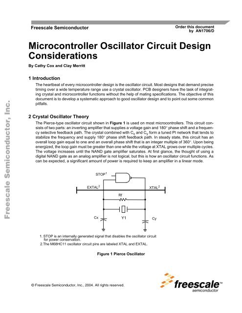
The Pierce-type oscillator circuit shown in Figure 1 is used on most microcontrollers. This circuit consists<br />
of two parts: an inverting amplifier that supplies a voltage gain and 180°<br />
phase shift and a frequency<br />
selective feedback path. The crystal combined with Cx<br />
and Cy<br />
form a tuned PI network that tends to<br />
stabilize the frequency and supply 180°<br />
phase shift feedback path. In steady state, this circuit has an<br />
overall loop gain equal to one and an overall phase shift that is an integer multiple of 360°<br />
. Upon being<br />
energized, the loop gain must be greater than one while the voltage at XTAL grows over multiple cycles.<br />
The voltage increases until the NAND gate amplifier saturates. At first glance, the thought of using a<br />
digital NAND gate as an analog amplifier is not logical, but this is how an oscillator circuit functions. As<br />
can be expected, a significant amount of power is required to keep an amplifier in a linear mode.<br />
EXTAL 2<br />
STOP 1<br />
Cx<br />
Rf<br />
Y1<br />
Figure 1 Pierce <strong>Oscillator</strong><br />
XTAL 2<br />
1. STOP is an internally generated signal that disables the oscillator circuit<br />
for power conservation.<br />
2.The M68HC11 oscillator circuit pins are labeled XTAL and EXTAL.<br />
Cy
Freescale Semiconductor, Inc...<br />
2<br />
Freescale Semiconductor, Inc.<br />
A crystal is a small wafer of high grade quartz cut at a certain angle and to a certain size. Thinner cuts<br />
give higher frequency crystals, approximately 0.15 mm at 15 MHz. Crystals are designed and manufactured<br />
to operate a the rated frequency with a certain load capacitance (CL).<br />
Typical load capacitance<br />
values are 12 pF, 15 pF, 18 pF, 20 pF, 22 pF and 32 pF. Metal leads are plated to the crystal for electrical<br />
connections. As a voltage potential is placed across the crystal element, the force of trapped electrons<br />
in the crystalline structure tends to deform the element. This is referred to as the piezoelectric<br />
effect. As the element flexes, electrical impedance changes. The crystal acts as an electro-mechanical<br />
device and can be modeled as a network of passive electrical components with a very sharp cutoff frequency.<br />
The physical properties of quartz make it very stable over both time and temperature.<br />
The usual model of a crystal is a network of two capacitors, an inductor and a resistor as shown in Figure<br />
2.<br />
The shunt capacitance (C0)<br />
is introduced by the metal plates used for electrical connections to<br />
the quartz wafer. Crystals are capable of oscillating at multiple frequencies. These frequencies are commonly<br />
referred to as overtones. For each overtone, a series RLC combination is added to the model. At<br />
the rated frequency of operation, the impedance of a crystal is inductive. As shown in Figure 3,<br />
the<br />
reactance of the crystal is capacitive up to a series resonant frequency (Fs)<br />
and beyond the anti-resonant<br />
frequency (Fa),<br />
the reactance is also capacitive. This means that the frequency of oscillation is<br />
bounded by Fs<br />
and Fa.<br />
The exact steady state frequency is determined by amplifier gain and load capacitance.<br />
Load capacitors (Cx<br />
and Cy)<br />
are used to form a tuned LC tank circuit in resonance. The combined capacitive<br />
impedance of Cx, Cy and other stray capacitance equals the inductive reactance of the crystal.<br />
Frequency of operation can be estimated by:<br />
f<br />
≈ 1 / [2∗<br />
π∗√(L1∗CL)]<br />
In many cases, the voltage at EXTAL and XTAL actually swings outside the ground and supply rails.<br />
Changing capacitance values will slightly change the operating frequency and can significantly change<br />
the voltage at EXTAL and XTAL. It is important to size these elements correctly and to use quality capacitors<br />
with long life, very low ESR, and good stability over temperature.<br />
(L1,C1 and R1 represent fundamental operating frequency. L2, C2, R2, L3, C3 and<br />
R3 represent overtone frequency operation.)<br />
C0<br />
Figure 2 Passive Element Modeling of Crystal<br />
L1<br />
L2<br />
L3<br />
C1<br />
C2<br />
C3<br />
For More Information On This Product,<br />
Go to: www.freescale.com<br />
R1<br />
R2<br />
R3<br />
<strong>AN1706</strong>/D
Freescale Semiconductor, Inc...<br />
Fs<br />
= Series Resonant Frequency. Fa<br />
= Antiresonant Frequency. (Note: Frequency axis is not drawn to scale.)<br />
<strong>AN1706</strong>/D<br />
Crystal Reactance<br />
Freescale Semiconductor, Inc.<br />
f s<br />
Figure 3 Plot of Crystal Reactance with Respect to Frequency<br />
Mathematically demonstrating how an oscillator circuit starts is very challenging due to non-linear characteristics<br />
of the system such as amplifier gain and crystal impedance. A number of papers have been<br />
written on this subject, but an extensive analysis of an MCU design is not normally done. In general<br />
terms, an external element must effectively commence oscillation by placing a time variant voltage<br />
across the crystal. This can happen in a number of ways including injection of power supply noise and<br />
the processor negating the STOP signal, but normally this occurs when supply voltage is applied. Once<br />
a small voltage is applied to the crystal, the NAND gate acts as an analog amplifier and a closed loop<br />
feedback system is formed. The crystal and load capacitors determine the oscillation frequency.<br />
The feedback resistance, Rf,<br />
tends to keep the input to the NAND gate biased around supply voltage<br />
divided by two. Rf<br />
must be sized to allow adequate feedback while not unduly loading the circuit. The<br />
microcontroller manufacturer normally suggests a range of acceptable values, usually between 100 kΩ<br />
and 22 MΩ.<br />
For low frequency circuits, the crystal impedance is relatively high and the value for Rf<br />
must<br />
also be high (10 MΩ<br />
for 32 kHz). For higher frequencies, Rf<br />
must be lower (100 kΩ<br />
for 10–20 MHz).<br />
The voltages at EXTAL and XTAL are usually distorted sine waves approximately 180°<br />
out of phase.<br />
These sine waves swing symmetrically around the supply voltage/2. Distortion can be attributed to<br />
NAND gate amplifier saturation and to intrinsic diodes clipping the signal at EXTAL. Figure 4 shows<br />
typical waveforms seen at XTAL and EXTAL. Note the amplitude and phase differences. Propagation<br />
delays in the amplifier add a few degrees of phase shift.<br />
For More Information On This Product,<br />
Go to: www.freescale.com<br />
f a<br />
f<br />
3
Freescale Semiconductor, Inc...<br />
4<br />
(Freq = 4 MHz, Microprocessor = M68HC11E9)<br />
Freescale Semiconductor, Inc.<br />
Figure 4 Scope Captures of Voltages at EXTAL (Top) and XTAL (Bottom)<br />
The STOP pin of the NAND gate in Figure 1 is asserted by the CPU to disable the oscillator for ultra<br />
low-power mode operation. In normal operation, the NAND gate acts as a small signal-inverting amplifier<br />
operating in a linear mode. For sake of digital analysis, the gate is modeled as shown in Figure 5.<br />
However, to fully understand the operation of the oscillator circuit, the small signal equivalent circuit<br />
model must be analyzed as shown in Figure 6.<br />
EXTAL<br />
Cin<br />
Ideal Inverting<br />
Amp<br />
Rout<br />
a) Digital representation b) Small signal representation<br />
Figure 5 Model of CMOS Logic Gate<br />
Cin<br />
For More Information On This Product,<br />
Go to: www.freescale.com<br />
Cout<br />
XTAL<br />
<strong>AN1706</strong>/D
Freescale Semiconductor, Inc...<br />
In order for the oscillator circuit to resonate in a stable manner, the absolute gain of the amplifier must<br />
be ≥1.<br />
This ideally should ensure that the output signal does not decay to zero. In its steady state condition<br />
the loop gain is equal to one.<br />
Vin<br />
(G = Open Loop Gain of Amplifier.)<br />
<strong>AN1706</strong>/D<br />
+<br />
–<br />
Figure 6 Small Signal Model of Inverting Amplifier and Crystal <strong>Circuit</strong><br />
Correct choice of Cx<br />
and Cy<br />
is paramount to oscillator start-up and steady state conditions. Imbalances<br />
in capacitive and inductive impedance can cause phase and amplitude problems in the feedback loop.<br />
Normally, Cx<br />
and Cy<br />
are equal, however, in some cases, if Cx<br />
is chosen to be slightly smaller than Cy,<br />
the voltage swing at EXTAL can be increased without compromising balance or introducing phase problems.<br />
Table 1 shows the effects of varying Cx<br />
and Cy.<br />
Values shown are for a 4.9 MHz crystal, a typical<br />
M68HC11 drive circuit, and Vdd = 5V.<br />
Table 1 Voltage Changes for Varying Stabilizing Capacitors Cx<br />
and Cy<br />
Cx= Cy= V@EXTAL Crystal Power Dissipation<br />
56 pF 56 pF 3.3 Vpp 100 μW<br />
33 pF 56 pF 8.0 Vpp 199 μW<br />
47 pF 56 pF 6.1 Vpp 207 μW<br />
68 pF 68 pF 2.8 Vpp 102 μW<br />
3 Amplifier Gain and Crystal Drive<br />
Freescale Semiconductor, Inc.<br />
+<br />
–<br />
Rout<br />
– G*Vin<br />
XTAL<br />
Cout Cy<br />
EXTAL<br />
The microcontroller’s amplifier gain is a critical element in the start-up of an oscillator. It must be large<br />
enough to drive the stabilizing network but if it is too robust there could be deleterious effects; namely,<br />
excess power consumption, high RF emissions, and, worst of all, an amplifier that will not start. It is not<br />
an easy task to make an amplifier ideal for oscillator operation from 1–10 MHz while keeping the noise<br />
and power consumption to a minimum.<br />
A fairly simple experiment can be run to determine actual gain. Pull the EXTAL pin from the circuit board<br />
and capacitively couple a 25–50 mV peak-to-peak sine wave at the rated frequency to EXTAL. With<br />
power supplied to the board and components inserted, measure the voltage level on the XTAL pin. Calculating<br />
the ratio Vout/Vin gives the loaded amplifier gain. This should give a close approximation of the<br />
actual small signal value required at start-up. If the loaded gain is under 1.5, it may be a good idea to<br />
investigate ways to reduce the amplifier’s load by resizing the stabilizing capacitors or possibly choosing<br />
a different crystal.<br />
For More Information On This Product,<br />
Go to: www.freescale.com<br />
L1<br />
Cx Cin<br />
5
Freescale Semiconductor, Inc...<br />
6<br />
Overdriving a crystal for an extended period of time can physically damage a crystal. Typical drive levels<br />
for crystals can vary from 1 μW<br />
(for small 32 kHz tuning fork crystals) to 5 mW (for a circular AT-cut type<br />
high frequency crystals). By calculating the RMS current flowing through the circuit and being given the<br />
maximum series resistance, the power can be calculated using the formula:<br />
2<br />
P = I R.<br />
3.1 Understanding Capacitive Coupling and Inductance of PCB Traces<br />
As PCB and semiconductor geometries get progressively smaller, the understanding and control of capacitive<br />
coupling becomes paramount. Capacitance for two parallel plates can be calculated using the<br />
following formula:<br />
Where:<br />
C (farads) = k<br />
ε0<br />
(A / d).<br />
ε<br />
12<br />
2<br />
2<br />
0 = Permitivity of Free space = 8.85 * 10 Coulombs /Newton * Meter<br />
A = Plate area<br />
d = Distance between plates<br />
k = Dielectric constant of material<br />
3.1.1 Example:<br />
Consider a trace 1.0 cm long by 0.1 cm wide sitting directly above a solid ground plane. The board is a<br />
two-layer FR4 type with a distance between copper layers being 0.031 cm. The dielectric constant of<br />
fiberglass is approximately 3.5.<br />
-12<br />
C = 3.5 * 8.85*10 * (.01m*.001m)/.00031m = 1 10-12<br />
F or 1 pF.<br />
With surface-mount devices, the pad area for components can actually increase and for multilayer<br />
boards the distance (d) can be very small. These factors can increase the board’s stray capacitance<br />
values into 5–10 pF range quite easily. For hybrid printed circuit boards, a very thin dielectric is<br />
screened between conducting layers. This can sometimes make the distance between layers 1–2 mils<br />
( 2.5–5 mm). The dielectric constant can be between 10–15, giving stray capacitance values between<br />
15–50 pF for even nominal pad and trace sizes.<br />
In regard to inductance, when current flows through any conductor there is some associated self inductance.<br />
The measured inductance is dependent on the current loop area. Having a large ground plane<br />
can usually guarantee the smallest loop area. Users of single layer boards and two layer boards without<br />
ground planes must take special precautions to keep the oscillator trace length as short as possible and<br />
with minimal loop area. Care should be taken to ensure the power source to the microcontroller is well<br />
decoupled.<br />
4 Potential Problem Areas<br />
Freescale Semiconductor, Inc.<br />
Increasing the capacitance from either leg of the crystal to ground through stray effects of board layout<br />
is not detrimental so long as it is taken into account when selecting the stabilizing capacitors Cx<br />
and Cy.<br />
Making the traces for Cx<br />
and Cy<br />
exceedingly long can add unwanted inductance. Figure 7 is a model<br />
of the effects of the PCB on the oscillator circuit. Inductance is a function of total area enclosed by a<br />
current loop. Make certain that the power supply and return paths are as short as possible and, more<br />
importantly, that the loop area of this path is as small as possible. Cx,<br />
Cy,<br />
Rf<br />
and the crystal should be<br />
placed as close as possible to the microcontroller’s oscillator pins.<br />
For More Information On This Product,<br />
Go to: www.freescale.com<br />
<strong>AN1706</strong>/D
Freescale Semiconductor, Inc...<br />
<strong>AN1706</strong>/D<br />
Rx1<br />
Rx2<br />
+5V<br />
Freescale Semiconductor, Inc.<br />
EXTAL<br />
Cx<br />
Lx<br />
Figure 7 Modeling of PCB Effects on <strong>Oscillator</strong> <strong>Circuit</strong><br />
The following problems have been witnessed by Freescale application engineers:<br />
Rf<br />
XTAL<br />
• Long trace leads:<br />
— Long trace leads and uncontrolled capacitive coupling can cause problems. Referring to Figure<br />
7,<br />
if L1<br />
or L2<br />
are any significant level, the net impedance of the Cx<br />
+Lx or Cy +Ly can be very<br />
small, effectively eliminating any feedback voltage. If there is any significant capacitance, the<br />
effective loading of the amplifier may be much more than calculated and the gain may not be<br />
sufficient. This is probably the number one problem encountered. Multilayer and hybrid PCBs<br />
can have substantial coupling to ground. See 5 Testing and Troubleshooting for more on<br />
this problem.<br />
• PCB contaminants:<br />
— PCB contaminants reducing impedance between nodes such as humidity, flux, and finger<br />
prints are problems. When printed circuit boards are manufactured, a flux is applied to the<br />
board to promote good solder bonds. Normally, a wash cycle is used to remove the flux. If the<br />
board is not cleaned entirely, the residual flux may supply an unwanted impedance path on the<br />
board. Take special care to check between the crystal leads and beneath SMT devices. These<br />
are notorious locations for flux build-up. Humidity or actual condensation on the board can also<br />
supply unwanted impedance paths. Referring to Figure 6 if Rx2 is introduced due to contaminants,<br />
the input offset voltage will be pulled towards ground. This will effectively lower the amplifiers<br />
gain by limiting the input voltage swing.<br />
• Power supply noise:<br />
— Power supply noise can sometimes be greatly amplified by the oscillator’s amplifier. If the power<br />
supply noise is some harmonic of the crystal frequency, or vice versa, the oscillator may not<br />
begin to oscillate. In other cases, it has been seen that a noise element on the power supply<br />
actually helped the circuit begin oscillating by supplying a much needed high frequency component.<br />
Tying the stabilizing capacitors to +5 V sometimes provides a better AC reference<br />
point than ground. A good test for this condition is to disable the board’s power supply and use<br />
a high-quality bench supply to power the board. If the oscillator starts with the bench supply<br />
but not with the board supply, look at cleaning up the +5 V rail. In most cases, if power supply<br />
noise is a problem, the voltage at XTAL will be a constant around V supply/2.<br />
• No operation at high temperature:<br />
— The crystal may not start at high temperatures. Usually this is caused by undue loading of the<br />
amplifier. Check on-board contaminants and the proper sizing of the stabilizing capacitors.<br />
Cy<br />
For More Information On This Product,<br />
Go to: www.freescale.com<br />
Ly<br />
+5V<br />
Ry1<br />
Ry2<br />
7
Freescale Semiconductor, Inc...<br />
8<br />
• Frequency instability:<br />
— Frequency instability is usually caused either by driving the crystal too hard or insufficiently due<br />
to incorrectly sized stabilizing capacitors. If prolonged, overdriving the crystal can cause permanent<br />
damage. See 3 Amplifier Gain and Crystal Drive for details on the drive level of the<br />
crystal. It should be noted that the size of the stabilizing capacitors controls the voltage across<br />
the crystal.<br />
• High frequency issues (>10 MHz):<br />
— A CMOS amplifier tends to have a gain attenuation as frequency increases. In most microcontrollers,<br />
the open loop gain of the amplifier is sufficiently above one at the maximum operating<br />
frequency to ensure good performance. However, feeding auxiliary microprocessors or other<br />
digital circuits can add sufficient load to swamp the amplifier and prevent oscillation. Also note<br />
that as the frequency becomes very large, the impedance of a capacitor decreases which can<br />
make stray capacitance a much greater problem.<br />
• Low frequency issues (
Freescale Semiconductor, Inc...<br />
A probe for most scopes may be modeled as shown in Figure 8. The 8–15 pF capacitor can load the<br />
circuit down considerably at high frequencies.<br />
Zin (Scope Probe)<br />
<strong>AN1706</strong>/D<br />
Freescale Semiconductor, Inc.<br />
1–10Mohm<br />
C = 8–12 pF<br />
Figure 8 <strong>Circuit</strong> Modeling of Oscilloscope and Probe Loading<br />
Table 2 Scope Probe Values<br />
f Zin (8 pF) Zin (15 pF)<br />
500 kHz 39.8 kΩ 21.2 kΩ<br />
1 MHz 19.9 kΩ 10.6 kΩ<br />
4 MHz 4.97 kΩ 2.65 kΩ<br />
16 MHz 1.24 kΩ 663 Ω<br />
50 MHz 398 Ω 212 Ω<br />
An active FET probe can be used to monitor the circuit without adversely affecting circuit parameters.<br />
These probes are quite expensive but have a very high input impedance. Typical FET probes have an<br />
input capacitance below 2 pF and input resistance above 5 MΩ.<br />
Sometimes the actual impedance of the probe is not as critical as the fact that the input signal is being<br />
pulled from the optimal 2.5 V center voltage. Balanced loading of probes with resistors and/or capacitors<br />
can sometimes allow a high-impedance circuit to be monitored with a standard oscilloscope.<br />
Different conditions can greatly impact start-up and steady state performance. Here are a few tests that<br />
can be performed to measure the robustness of your design.<br />
1. Vary the input voltage from 3 to 5.5 V. The circuit should start oscillating and the frequency<br />
should rise slightly as the voltage is increased. If it actually decreases as the voltage is increased,<br />
there is a good chance that the crystal is being dangerously overdriven. If no oscillation<br />
occurs, the feedback resistor may need to be made smaller.<br />
2. Control the rise time of the power supply. An empirical formula for the frequency content of a<br />
rising edge is given:<br />
fmax approx = (1/(π*risetime))<br />
R = 50 ohms<br />
Having a very fast-rising power supply might stimulate the crystal at the resonant frequency!!<br />
3. Placing a 1k potentiometer in series with the crystal can give some information about amplifier<br />
tolerance. With added resistance, the circuit will be less likely to start. Slowly increase the resistance<br />
from 0 Ω. After each increment, remove power from the board and re-energize it . Note<br />
the value of the potentiometer when the circuit will not start. The resistance (crystal + potentiometer)<br />
is substantially larger than the worst-case resistance specified by the crystal manufacturer.<br />
In order to allow for circuit variations, it is desirable to have the circuit oscillate with two<br />
times the maximum crystal resistance. (The resistance value for the potentiometer should increase<br />
as crystal frequency is decreased. i.e., 10 MHz =>1kΩ, 32 kHz => 10 kΩ.)<br />
4. Test under cold, hot, and high humidity conditions. Resistance increases with temperature. Increasing<br />
source resistance reduces the effective loop gain. Any time the oscillator will not start<br />
or major frequency shifts occur, a problem exists.<br />
For More Information On This Product,<br />
Go to: www.freescale.com<br />
9
Freescale Semiconductor, Inc...<br />
10<br />
5. Run worst-case loading conditions on the power portion of the board. Drive inductive loads<br />
such as relays, solenoids and motors under full load conditions. In certain circumstances, the<br />
magnetic field or the electric field can couple into the relatively high impedance oscillator causing<br />
transients. This can sometimes be detected by the microprocessor’s software running into<br />
confusion due to a very short clock pulse not being properly recognized by the CPU.<br />
6. Check board capacitance using this test. Measure the exact frequency of the crystal with a<br />
tightly controlled load capacitance on a separate apparatus. Then, measure the frequency on<br />
the actual PCB. If the two do not correlate well, unknown stray capacitance may exist on the<br />
board and the stabilizing capacitors may need to be reduced.<br />
One last note, if the circuit does not commence oscillating when the circuit is energized, check the voltages<br />
at EXTAL and XTAL. If one is high and one is low, stray impedances are probably present causing<br />
unwanted coupling between crystal leads, either to ground or to the power rail. If the voltage at EXTAL<br />
is a +2.5 VDC, the feedback resistor is insufficient or a severe noise element is present on the power<br />
or ground rails.<br />
6 Conclusions<br />
Freescale Semiconductor, Inc.<br />
This document has given a basic explanation of how and why a crystal oscillator circuit operates. Suggestions<br />
have been given on how to size circuit components, and how to test the circuit’s robustness.<br />
Some of the design and implementation problems experienced by Freescale application engineers have<br />
been discussed in the hope of preventing similar problems from occurring in the future.<br />
Many assumptions about modeling have been made in the analysis of oscillator circuits. Most of the<br />
assumptions have been empirically proven but this document does not attempt to stringently perform<br />
mathematical derivations. Many of the circuit elements change non-linearly over frequency, loading,<br />
and temperature (i.e., crystal impedance and amplifier gain) making precise modeling a non-trivial task.<br />
7 References<br />
1. Burch, Ken, XTAL. 1992<br />
2. KDS America, KDS Crystal Catalog. 1995<br />
3. Van Doren, Dr. Tom, Grounding and Shielding Electronic Systems.<br />
4. VX Kyocera, Timing Devices.<br />
5. Sears, Francis, University Physics. 1982.<br />
6. Landee, Robert, Electronics <strong>Design</strong>ers’ Handbook. McGraw-Hill, 1977<br />
7. Frerking, Marvin, Crystal <strong>Oscillator</strong> <strong>Design</strong> and Temperature Compensation. Van Nostrand<br />
Reinhold, 1978.<br />
8. Freescale Component Product Division, Product Catalog. 1994.<br />
9. Fox Electronics, Frequency Control Products. Volume 15 Number 1994.<br />
APPENDIX A Crystal Versus Resonator Issues<br />
Resonators are a lower-cost, less exact alternative to crystals. Instead of a quartz crystal element, resonators<br />
make use of other piezoelectric crystalline structures such as barium titanate. This allows the<br />
element to be smaller, less expensive, and to have improved start-up times. The surrounding circuitry<br />
is identical to that of a crystal with a parallel resistor to help in the start-up phase and with stabilizing<br />
capacitors on both legs to ground (see Figure 1).<br />
For a given frequency, the required stabilizing capacitors are usually much larger for a resonator. This<br />
means that a slightly larger amplifier drive capability is needed which will tend to consume more power.<br />
Resonators in general are not offered below 125 kHz but are available up to 20 MHz.<br />
For More Information On This Product,<br />
Go to: www.freescale.com<br />
<strong>AN1706</strong>/D
Freescale Semiconductor, Inc...<br />
APPENDIX B AT-Strip Crystals.<br />
The “AT” in AT-cut and AT-strip crystals specifies the angle of cut relative to the Z-axis to be 35 degrees.<br />
AT-cut crystals are thin, circular disks of quartz while AT-strip crystals are thin, rectangular pieces of<br />
quartz (the width is very small compared to the length). AT-cut crystals will fit in smaller packages and<br />
require less quartz which should make them less expensive.<br />
AT-strip crystals function identically to the AT-cut type and the same Pierce oscillator circuit configuration<br />
is used. However, the smaller piece of quartz is not as resistant to mechanical shock or to excess<br />
electrical drive. Care should be taken to calculate the drive level and ensure stabilizing capacitors<br />
are sized appropriately. In general, for any given frequency, the series resistance and the maximum<br />
drive of an AT-strip crystal will be lower than that of an AT-cut crystal. (i.e., 4 MHz AT-cut: max ESR =<br />
120 Ω, max drive = 5 mW; 4 MHz AT-strip: max ESR = 40 Ω, max drive = 1 mW)<br />
The M68HC11 reference manual contains a statement warning against the use of AT-strip type crystals.<br />
This statement was made when AT-strip crystals were just being developed and the drive level was<br />
thought to be much lower than those specified today. There are many successful designs in production<br />
using AT-strip crystals with M68HC11’s. <strong>Design</strong>ers should not be inhibited from using either a ceramic<br />
resonator, AT-strip, or AT-cut crystals in their microcontroller application.<br />
APPENDIX C 32-kHz Operation Specifics<br />
The basic theory behind the operation of a low-frequency crystal is identical to that listed in earlier sections.<br />
The big difference is that relative impedances are much higher for low-frequency operation. In<br />
many cases, a resistor needs to be inserted in series with the crystal to keep it from being overdriven.<br />
See Figure 9. The correct placement of this resistor is very important. Do not place Rs on the amplifier’s<br />
input side. Also, Rf should feed directly back from XTAL to EXTAL. Rs will range from 100 Ω to 330 kΩ<br />
depending upon Vdd, the crystal frequency, and the amplifier’s drive.<br />
<strong>AN1706</strong>/D<br />
Freescale Semiconductor, Inc.<br />
Table 3 Table of Characteristics<br />
Characteristic Resonator Crystal<br />
Cost Inexpensive High<br />
Freq Control ± 0.5% ±0.002 %<br />
Temp. Range –40 to 125 °C –40 to 125 °C<br />
Ease of Start Easy Hard to analyze<br />
Package Both available in thru-hole and SMT<br />
STOP<br />
EXTAL XTAL<br />
Cx<br />
Rf<br />
Y1<br />
Figure 9 Typical <strong>Oscillator</strong> <strong>Circuit</strong> for Low Frequency Crystals<br />
For More Information On This Product,<br />
Go to: www.freescale.com<br />
Cy<br />
11
Freescale Semiconductor, Inc...<br />
Freescale Semiconductor, Inc.<br />
Phase-locked loops are control circuits that depend upon negative feedback for stability. This means<br />
that the output frequency will always contain small deviations from the desired frequency. In most<br />
Freescale microcontrollers using PLLs, separate power and ground pins are supplied for the PLL. These<br />
pins need a separate high-quality decoupling capacitor to eliminate any noise for this very sensitive circuit.<br />
Even more important is a pin labeled “XFC.” This is for connection of a high-quality 0.1 μF capacitor<br />
to act as a filter in the PLL’s feedback. If nothing is connected, or a capacitor with a high ESR is used,<br />
the PLL probably will not lock.<br />
For microprocessors utilizing phase-locked loops (PLLs), a parameter called “jitter” needs to be specified.<br />
Jitter, or clock stability, is defined as the variance in maximum frequency over a specified time period.<br />
For a 16.7-MHz system, jitter can vary by up to 100 kHz for any given five microsecond window.<br />
However, over a longer window of time, say one millisecond, the average frequency can be controlled<br />
to +/– 0.05%. Variation of crystal frequency would also need to be included in the timer system absolute<br />
error.


