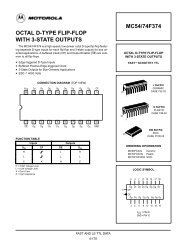
74F74 Dual D-Type Positive Edge-Triggered Flip-Flop
74F74 Dual D-Type Positive Edge-Triggered Flip-Flop
74F74 Dual D-Type Positive Edge-Triggered Flip-Flop

You also want an ePaper? Increase the reach of your titles
YUMPU automatically turns print PDFs into web optimized ePapers that Google loves.
<strong>74F74</strong><strong>Dual</strong> D-<strong>Type</strong> <strong>Positive</strong> <strong>Edge</strong>-<strong>Triggered</strong> <strong>Flip</strong>-<strong>Flop</strong>General DescriptionThe F74 is a dual D-type flip-flop with Direct Clear and Setinputs and complementary (Q, Q) outputs. Information atthe input is transferred to the outputs on the positive edgeof the clock pulse. Clock triggering occurs at a voltage levelof the clock pulse and is not directly related to the transitiontime of the positive-going pulse. After the Clock Pulse inputthreshold voltage has been passed, the Data input islocked out and information present will not be transferred toOrdering Code:April 1988Revised July 1999the outputs until the next rising edge of the Clock Pulseinput.Asynchronous Inputs:LOW input to S D sets Q to HIGH levelLOW input to C D sets Q to LOW levelClear and Set are independent of clockSimultaneous LOW on C D and S Dmakes both Q and Q HIGHOrder Number Package Number Package Description<strong>74F74</strong>SC M14A 14-Lead Small Outline Integrated Circuit (SOIC), JEDEC MS-120, 0.150 Narrow<strong>74F74</strong>SJ M14D 14-Lead Small Outline Package (SOP), EIAJ TYPE II, 5.3mm Wide<strong>74F74</strong>PC N14A 14-Lead Plastic <strong>Dual</strong>-In-Line Package (PDIP), JEDEC MS-001, 0.300 WideDevices also available in Tape and Reel. Specify by appending the suffix letter “X” to the ordering code.<strong>74F74</strong> <strong>Dual</strong> D-<strong>Type</strong> <strong>Positive</strong> <strong>Edge</strong>-<strong>Triggered</strong> <strong>Flip</strong>-<strong>Flop</strong>Logic SymbolsConnection DiagramIEEE/IEC© 1999 Fairchild Semiconductor Corporation DS009469 www.fairchildsemi.com
Absolute Maximum Ratings(Note 1)Storage Temperature−65°C to +150°CAmbient Temperature under Bias −55°C to +125°CJunction Temperature under Bias −55°C to +150°CV CC Pin Potential to Ground Pin−0.5V to +7.0VInput Voltage (Note 2)−0.5V to +7.0VInput Current (Note 2)−30 mA to +5.0 mAVoltage Applied to Outputin HIGH State (with V CC = 0V)Standard Output−0.5V to V CC3-STATE Output−0.5V to +5.5VCurrent Applied to Outputin LOW State (Max)twice the rated I OL (mA)ESD Last Passing Voltage (Min)4000VRecommended OperatingConditionsFree Air Ambient TemperatureSupply Voltage0°C to +70°C+4.5V to +5.5VNote 1: Absolute maximum ratings are values beyond which the devicemay be damaged or have its useful life impaired. Functional operationunder these conditions is not implied.Note 2: Either voltage limit or current limit is sufficient to protect inputs.<strong>74F74</strong>DC Electrical CharacteristicsSymbol Parameter Min Typ Max Units V CC ConditionsV IH Input HIGH Voltage 2.0 V Recognized as a HIGH SignalV IL Input LOW Voltage 0.8 V Recognized as a LOW SignalV CD Input Clamp Diode Voltage −1.2 V Min I IN = −18 mAV OH Output HIGH 10% V CC 2.5I OH = −1 mAV MinVoltage 5% V CC 2.7 I OH = −1 mAV OL Output LOW 10% V CC 0.5 V Min I OL = 20 mAVoltageI IH Input HIGHCurrent5.0 µA Max V IN = 2.7VI BVI Input HIGH CurrentBreakdown Test7.0 µA Max V IN = 7.0VI CEX Output HIGHLeakage Current50 µA Max V OUT = V CCV ID Input LeakageI ID = 1.9 µA4.75 V 0.0TestAll Other Pins GroundedI OD Output LeakageV IOD = 150 mV3.75 µA 0.0Circuit CurrentAll Other Pins GroundedI IL Input LOW Current −0.6V IN = 0.5V (D, CP)−1.8mA MaxV IN = 0.5V (C D , S D )I OS Output Short-Circuit Current −60 −150 mA Max V OUT = 0VI CC Power Supply Current 10.5 16.0 mA Max3 www.fairchildsemi.com
<strong>74F74</strong>AC Electrical CharacteristicsT A = +25°CT A = 0°C to +70°CV CC = +5.0VV CC = +5.0VSymbolParameterUnitsC L = 50 pFC L = 50 pFMin Typ Max Min Maxf MAX Maximum Clock Frequency 100 125 100 MHzt PLH Propagation Delay 3.8 5.3 6.8 3.8 7.8t PHL CP n to Q n or Q n4.4 6.2 8.0 4.4 9.2nst PLH Propagation Delay 3.2 4.6 6.1 3.2 7.1t PHL C Dn or S Dn to Q n or Q n 3.5 7.0 9.0 3.5 10.5nsAC Operating RequirementsT A = +25°C T A = 0°C to +70°CSymbolParameterV CC = +5.0VV CC = +5.0V UnitsMin Max Min Maxt S (H) Setup Time, HIGH or LOW 2.0 2.0t S (L) D n to CP n 3.0 3.0t H (H) Hold Time, HIGH or LOW 1.0 1.0nst H (L) D n to CP n 1.0 1.0t W (H) CP n Pulse Width 4.0 4.0t W (L) HIGH or LOW 5.0 5.0nst W (L) C Dn or S Dn Pulse Width 4.0 4.0 nsLOWt REC Recovery Time 2.0 2.0 nsC Dn or S Dn to CPwww.fairchildsemi.com 4
Physical Dimensions inches (millimeters) unless otherwise noted<strong>74F74</strong>14-Lead Small Outline Integrated Circuit (SOIC), JEDEC MS-120, 0.150 NarrowPackage Number M14A14-Lead Small Outline Package (SOP), EIAJ TYPE II, 5.3mm WidePackage Number M14D5 www.fairchildsemi.com
<strong>74F74</strong> <strong>Dual</strong> D-<strong>Type</strong> <strong>Positive</strong> <strong>Edge</strong>-<strong>Triggered</strong> <strong>Flip</strong>-<strong>Flop</strong>Physical Dimensions inches (millimeters) unless otherwise noted (Continued)14-Lead Plastic <strong>Dual</strong>-In-Line Package (PDIP), JEDEC MS-001, 0.300 WidePackage Number N14AFairchild does not assume any responsibility for use of any circuitry described, no circuit patent licenses are implied andFairchild reserves the right at any time without notice to change said circuitry and specifications.LIFE SUPPORT POLICYFAIRCHILD’S PRODUCTS ARE NOT AUTHORIZED FOR USE AS CRITICAL COMPONENTS IN LIFE SUPPORTDEVICES OR SYSTEMS WITHOUT THE EXPRESS WRITTEN APPROVAL OF THE PRESIDENT OF FAIRCHILDSEMICONDUCTOR CORPORATION. As used herein:1. Life support devices or systems are devices or systemswhich, (a) are intended for surgical implant into thebody, or (b) support or sustain life, and (c) whose failureto perform when properly used in accordance withinstructions for use provided in the labeling, can be reasonablyexpected to result in a significant injury to theuser.www.fairchildsemi.com 62. A critical component in any component of a life supportdevice or system whose failure to perform can be reasonablyexpected to cause the failure of the life supportdevice or system, or to affect its safety or effectiveness.www.fairchildsemi.com