AN3115, Implementing a Digital AC/DC Switched-Mode ... - Freescale
AN3115, Implementing a Digital AC/DC Switched-Mode ... - Freescale
AN3115, Implementing a Digital AC/DC Switched-Mode ... - Freescale
Create successful ePaper yourself
Turn your PDF publications into a flip-book with our unique Google optimized e-Paper software.
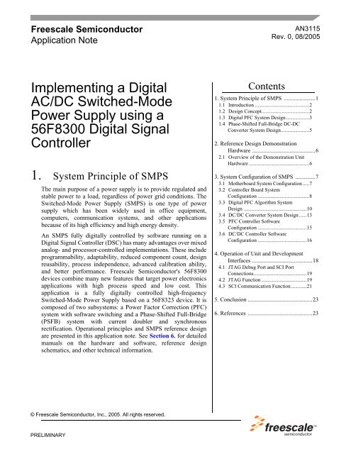
<strong>Freescale</strong> Semiconductor<br />
Application Note<br />
<strong>Implementing</strong> a <strong>Digital</strong><br />
<strong>AC</strong>/<strong>DC</strong> <strong>Switched</strong>-<strong>Mode</strong><br />
Power Supply using a<br />
56F8300 <strong>Digital</strong> Signal<br />
Controller<br />
1. System Principle of SMPS<br />
The main purpose of a power supply is to provide regulated and<br />
stable power to a load, regardless of power grid conditions. The<br />
<strong>Switched</strong>-<strong>Mode</strong> Power Supply (SMPS) is one type of power<br />
supply which has been widely used in office equipment,<br />
computers, communication systems, and other applications<br />
because of its high efficiency and high energy density.<br />
An SMPS fully digitally controlled by software running on a<br />
<strong>Digital</strong> Signal Controller (DSC) has many advantages over mixed<br />
analog- and processor-controlled implementations. These include<br />
programmability, adaptability, reduced component count, design<br />
reusability, process independence, advanced calibration ability,<br />
and better performance. <strong>Freescale</strong> Semiconductor's 56F8300<br />
devices combine many new features that target power electronics<br />
applications with high process speed and low cost. This<br />
application is a fully digitally controlled high-frequency<br />
<strong>Switched</strong>-<strong>Mode</strong> Power Supply based on a 56F8323 device. It is<br />
composed of two subsystems: a Power Factor Correction (PFC)<br />
system with software switching and a Phase-Shifted Full-Bridge<br />
(PSFB) system with current doubler and synchronous<br />
rectification. Operational principles and SMPS reference design<br />
are presented in this application note. See Section 6. for detailed<br />
manuals on the hardware and software, reference design<br />
schematics, and other technical information.<br />
© <strong>Freescale</strong> Semiconductor, Inc., 2005. All rights reserved.<br />
PRELIMINARY<br />
Contents<br />
<strong>AN3115</strong><br />
Rev. 0, 08/2005<br />
1. System Principle of SMPS ......................1<br />
1.1 Introduction ..........................................2<br />
1.2 Design Concept.....................................2<br />
1.3 <strong>Digital</strong> PFC System Design..................3<br />
1.4 Phase-Shifted Full-Bridge <strong>DC</strong>-<strong>DC</strong><br />
Converter System Design......................5<br />
2. Reference Design Demonstration<br />
Hardware ............................................6<br />
2.1 Overview of the Demonstration Unit<br />
Hardware...............................................6<br />
3. System Configuration of SMPS ..............7<br />
3.1 Motherboard System Configuration .....7<br />
3.2 Controller Board System<br />
Configuration ........................................8<br />
3.3 <strong>Digital</strong> PFC Algorithm System<br />
Design .................................................10<br />
3.4 <strong>DC</strong>/<strong>DC</strong> Converter System Design......13<br />
3.5 PFC Controller Software<br />
Configuration ......................................15<br />
3.6 <strong>DC</strong>/<strong>DC</strong> Controller Software<br />
Configuration ......................................16<br />
4. Operation of Unit and Development<br />
Interfaces ..........................................18<br />
4.1 JTAG Debug Port and SCI Port<br />
Connections.........................................19<br />
4.2 JTAG Function ...................................19<br />
4.3 SCI Communication Function ............21<br />
5. Conclusion .............................................23<br />
6. References .............................................23
System Principle of SMPS<br />
1.1 Introduction<br />
By using full digital control, an SMPS system becomes flexible and can also realize complex control arithmetic<br />
that improves efficiency and lowers cost. A controller-based SMPS system integrates high-performance digital<br />
signal processing with power electronics, providing a new method for design of power electronics, and the<br />
typical high-level control and communication capability an SMPS system requires. This reference design uses<br />
the <strong>Freescale</strong> 56F8323 device to perform input power factor correction and phase-shifted, full-bridge <strong>DC</strong>/<strong>DC</strong><br />
power conversion, providing excellent efficiency, low cost, and design flexibility.<br />
1.2 Design Concept<br />
The system comprises two parts: the primary side is the <strong>AC</strong>/<strong>DC</strong> converter with PFC; the secondary side is a<br />
full-bridge <strong>DC</strong>/<strong>DC</strong> converter. The <strong>AC</strong>/<strong>DC</strong> system uses an interleaved PFC boost control structure, which<br />
includes a full-bridge rectifier, two interleaved parallel BOOST PFC circuits, and two assistant switches to<br />
realize the Zero Voltage Switch (ZVS) of the main switches. By implementing a ZVS algorithm, the<br />
components' stress is reduced, and efficiency is improved, which allows the design to eliminate the reverse<br />
recovery output diodes. The <strong>DC</strong>/<strong>DC</strong> converter uses a ZVS phase-shifted full-bridge control structure<br />
implemented in software with a current doubler rectifier. This reduces the size of the filter inductor and<br />
improves efficiency. The high-level functional and performance requirements of the design include:<br />
Input voltage: 85V <strong>AC</strong>—265V <strong>AC</strong><br />
Input frequency: 45Hz—65Hz<br />
PFC switch frequency: 100KHz<br />
<strong>DC</strong>Bus voltage: 380V<br />
Input Power Factor (PF): >0.99<br />
<strong>DC</strong>/<strong>DC</strong> switch frequency: 150KHz<br />
Output voltage: 48V <strong>DC</strong><br />
Maximum output power: 500W<br />
A circuit diagram for a 56800/E-based <strong>Switched</strong>-<strong>Mode</strong> Power Supply (SMPS) is shown in Figure 1-1. The<br />
entire system is controlled by two 56F8323 devices. The primary-side device accomplishes all control of the<br />
PFC system, which includes the two main switches and two ZVS switches. The secondary-side device<br />
ccomplishes all control of the <strong>DC</strong>/<strong>DC</strong> phase-shifted full-bridge converter, which includes four main switches<br />
and two synchronous rectifiers. The functions performed in software for the PFC and <strong>DC</strong>/<strong>DC</strong> converter<br />
include: two digital PI regulators in the power system, control of all switches, soft start, digital generation of<br />
sine reference for the primary PFC, communication, power supply protection, and supervisor functions.<br />
<strong>Implementing</strong> a <strong>Digital</strong> <strong>AC</strong>/<strong>DC</strong> SMPS using a 56F8300 Device, Rev. 0<br />
2 <strong>Freescale</strong> Semiconductor<br />
Preliminary
<strong>AC</strong><br />
<strong>AC</strong><br />
L<br />
D<br />
R<br />
R<br />
lf1 Vf<br />
R<br />
Vsychr<br />
FUSE<br />
FUSE<br />
Q1A Q2A<br />
JP JP JP JP<br />
L1B L2B<br />
D1B<br />
C1 C2<br />
Q1B Q2B<br />
A<strong>DC</strong> PWM0 PWM3 TC0 TC1<br />
MC56F8323<br />
SPI/SCI<br />
D1C<br />
<strong>AC</strong>/<strong>DC</strong> Conversion with<br />
Power Factor Correction<br />
1.3 <strong>Digital</strong> PFC System Design<br />
D2C<br />
D1A<br />
D2A<br />
D2B<br />
R<br />
C +<br />
R<br />
Figure 1-1. <strong>AC</strong>/<strong>DC</strong> SMPS Block Diagram<br />
<strong>Implementing</strong> a <strong>Digital</strong> <strong>AC</strong>/<strong>DC</strong> SMPS using a 56F8300 Device, Rev. 0<br />
<strong>Digital</strong> PFC System Design<br />
The main circuit comprises two interleaved single-switch PFC circuits in which the two switches operate in an<br />
interleaved mode. The circuit, shown in Figure 1-2, is composed of Q1/Q2, D1/D2, L1/L2, and filter<br />
capacitance C. This portion implements the EMI filter, input relay, and full wave rectifier functions. To realize<br />
the ZVS of the two main switches, two assistant switches, VT3/VT4, and their assistant networks are included<br />
in the circuit design.<br />
<strong>Freescale</strong> Semiconductor 3<br />
Preliminary<br />
Q<br />
Q<br />
T<br />
Q<br />
Q<br />
ISO<br />
ISO<br />
Isolation<br />
T<br />
F<br />
T1<br />
Q<br />
Q<br />
PWM2—5<br />
L1C<br />
D<br />
D<br />
L2C<br />
C +<br />
lf2 lf1 vf<br />
PWM0 PWM1 A<strong>DC</strong><br />
R<br />
L<br />
MC56F8323<br />
SPI/SCI<br />
C +<br />
<strong>DC</strong>/<strong>DC</strong> Conversion using Soft<br />
Switching Technology<br />
R<br />
R<br />
Vo<br />
F
System Principle of SMPS<br />
Figure 1-2. PFC Block Diagram<br />
In the 56F8323-based PFC module system, the controller samples the voltage signal, V rect, from the full-wave<br />
rectifier, input current, I in , and output voltage, V bus ; the three analog signals are converted to digital samples by<br />
the 56F8323. Control arithmetic uses these signals in two loops to perform the PFC and rectification functions.<br />
An outer voltage loop, G 1, insures the output voltage is held constant. The output of the voltage loop<br />
determines the reference shape of the current loop, which guarantees the input current will be a sine wave. The<br />
sample of the input voltage determines the input current's crossing point, and is also used as a input feed<br />
forward voltage to accelerate the system response speed to input changes. The speed of the inner current loop,<br />
G 2 , is therefore more rapid. The current loop, G 2 , compares the current sample with current reference,<br />
calculates the duty parameters through the current loop PI regulator and controls the circuit through the<br />
PWM1/2 control signals to achieve the aim of PFC and stabilize the output voltage.<br />
Zero Voltage Transition (ZVT) technology is used to realize the ZVS of the main switch and the Zero Current<br />
Switch (ZCS) of boost diode so as to reduce the di/dt of the diode, which consequently reduces the switching<br />
loss and reduces the EMI radiation of the system. The theory of operation is realizing the ZVS of main<br />
switches by paralleling a capacitance in every switch’s drain-source to limit the switch’s dv/dt. Before the main<br />
switch transitions, the charge on capacitance is released to zero through assistant circuits to realize the ZVS of<br />
main switches. The assistant circuit effect is stopped as soon as the main switch ZVS occurs. That is, the<br />
assistant circuit operates for a short time before the main switch turns on.<br />
<strong>Implementing</strong> a <strong>Digital</strong> <strong>AC</strong>/<strong>DC</strong> SMPS using a 56F8300 Device, Rev. 0<br />
4 <strong>Freescale</strong> Semiconductor<br />
Preliminary
1.4 Phase-Shifted Full-Bridge <strong>DC</strong>-<strong>DC</strong> Converter System Design<br />
<strong>Implementing</strong> a <strong>Digital</strong> <strong>AC</strong>/<strong>DC</strong> SMPS using a 56F8300 Device, Rev. 0<br />
Phase-Shifted Full-Bridge <strong>DC</strong>-<strong>DC</strong> Converter System Design<br />
The phase-shifted full-bridge <strong>DC</strong>/<strong>DC</strong> converter combines the advantages of quasi-resonant technology and<br />
traditional PWM technology. It has a fixed frequency, and utilizes the LC-resonant energy to realize ZVS of<br />
main switches. It has the advantages of being easy to control with little switching loss and high reliability. In<br />
addition, the application uses a current doubler with synchronous rectifier topology, which brings several<br />
advantages, such as little duty loss, no reverse recovery and less difference to realize ZVS between two legs in<br />
comparison to a traditional full-wave rectifier.<br />
Figure 1-3 shows the main circuit, which is composed of four switches, (Q 1 —Q 4 ), transformer (T r ),<br />
capacitance (C r ). To prevent the transformer from saturating, it includes the secondary synchronous rectifier<br />
(Q 5 and Q 6 ), filter inductor (L f1 and L f2 ), and output filter capacitance (C f ). The input voltage is 380V <strong>DC</strong>, with<br />
the PWM switching frequency of 150KHz. Ignoring the dead time, the two switches operate at 180º<br />
complementary to each other. Constant output is achieved through adjusting the value of the phase shift<br />
between the switch pairs. When a = 0º, the Q 1 /Q 4 or Q 2 /Q 3 switch pairs are on simultaneously and the output<br />
value is at its maximum. When a = 180º, Q 1 /Q 2 or Q 3 /Q 4 are on simultaneously and the output voltage is zero.<br />
Three signals, the output voltage (V o ), primary inductor current (i L ) and output current (i o ), are routed to the<br />
secondary device’s A<strong>DC</strong> inputs. The sample signal of the inductor current is also routed to a hardware protect<br />
circuit, which is connected to the FAULT0 input of the processor. The software in the controller implements a<br />
voltage loop and a current loop as the basis of the control algorithm. In the control software, an error signal is<br />
generated by the comparison between the reference and the sampled value of the output voltage. The voltage<br />
loop comprises a PI regulator; its input is the error signal. The output of the voltage loop acts as the reference<br />
for the current loop; the error signal between primary inductor current and its reference acts as the input of<br />
current loop's PI regulator. Current loop outputs from the PI regulator are the control signal for the<br />
phase-shifted a. The 56F8323’s PWM1—PWM4 output the drive signal whose dead time and duty have been<br />
fixed, and according to a, adjust the value of phase shifted in order to stabilize the output voltage. From the<br />
relationship between the synchronous signal and primary drive signal, the synchronous drive signal can be<br />
derived easily. The software of the digital <strong>DC</strong>/<strong>DC</strong> converter also drives the LED circuits to show the output<br />
voltage value, protects the output current and communicates with the PC.<br />
<strong>Freescale</strong> Semiconductor 5<br />
Preliminary
Reference Design Demonstration Hardware<br />
Figure 1-3. <strong>Digital</strong>ly Controlled PSFB Converter Block Diagram<br />
2. Reference Design Demonstration Hardware<br />
2.1 Overview of the Demonstration Unit Hardware<br />
The demonstration unit is constructed with Printed Circuits Boards (PCB), active and passive components, and<br />
heatsink, all placed in a Plexiglas demonstration case. There is one input power plug on the right side of the<br />
unit, one output load connector on its left side, and one start button on the front.<br />
In the demonstration box, there are three layers in longitudinal direction: the bottom layer is heatsink, the<br />
middle is the power motherboard, and the top layer is two controller boards using 56F8323 devices. See<br />
Figure 2-1 for a photo of the demonstration box and Figure 2-2 for a drawing detailing the three layers.<br />
<strong>Implementing</strong> a <strong>Digital</strong> <strong>AC</strong>/<strong>DC</strong> SMPS using a 56F8300 Device, Rev. 0<br />
6 <strong>Freescale</strong> Semiconductor<br />
Preliminary
MotherBoard<br />
Motherboard<br />
Heatsink<br />
Figure 2-1. SMPS Demonstration Unit (Top View)<br />
Figure 2-2. SMPS Demonstration Unit Diagram<br />
3. System Configuration of SMPS<br />
3.1 Motherboard System Configuration<br />
<strong>Implementing</strong> a <strong>Digital</strong> <strong>AC</strong>/<strong>DC</strong> SMPS using a 56F8300 Device, Rev. 0<br />
Motherboard System Configuration<br />
56F8323 DSP Controller Controllers<br />
Board<br />
The SMPS hardware system consists of the power entry circuit, the Assistant Power Circuit (APC), the PFC<br />
primary-side circuit, the <strong>DC</strong>/<strong>DC</strong> secondary-side circuit, and the SCI communication circuit between the two.<br />
The PFC section includes the PFC driver circuit, PFC main circuit, and PFC analog signal sample circuit. The<br />
<strong>DC</strong>/<strong>DC</strong> function consists of the <strong>DC</strong>/<strong>DC</strong> driver circuit, <strong>DC</strong>/<strong>DC</strong> main power circuit, and the <strong>DC</strong>/<strong>DC</strong> analog<br />
signal sample circuit. To support future expansion, there is a second optocoupler driver circuit, which is<br />
<strong>Freescale</strong> Semiconductor 7<br />
Preliminary
System Configuration of SMPS<br />
compatible with a varied duty driver signal as well as the corresponding driver power supply circuit. These two<br />
components are not installed in the demonstration hardware. Detailed schematics are shown and described in<br />
the Designer Reference Manual; see Section 6.<br />
The functional regions of the power supply mother board are shown in Figure 3-1. The APC circuit provides<br />
several output voltage levels for the SMPS control system power, including +5V/+12V/-12V power for the<br />
primary side, and +5V/+12V/-12V/+20V power for the secondary side. The PFC circuit supplies three signals<br />
to the device’s A<strong>DC</strong> peripheral, the input current (I i ), the input voltage (V i ), and the output bus voltage (V bus ),<br />
that are used by the PFC software control algorithm. A relay controls the power entry, which realizes the main<br />
power circuit switch controlled by the 56F8323. The PFC main power circuit consists of two interleaved<br />
branch boost circuits; the PFC ZVS circuit is the accessory circuit to realize the ZVS of the main switch and<br />
the ZCS of boost diode reduces the di/dt of the diode. The driver circuits for the PFC system and the PFC ZVS<br />
system are implemented using the IR2125 special driver Integrated Circuit (IC).<br />
Figure 3-1. Functional Regions of the Main Motherboard<br />
3.2 Controller Board System Configuration<br />
The entire system consists of two parts: the Power Factor Correction (PFC) circuit and the <strong>DC</strong>/<strong>DC</strong> conversion<br />
circuit. The controller boards are used to control these two parts of the system. Each controller card is identical,<br />
but the processors run different software.<br />
The controller board includes six subsystems:<br />
1. CPU circuit<br />
2. A<strong>DC</strong> circuit<br />
3. Power supply circuit<br />
<strong>DC</strong>/<strong>DC</strong><br />
Synchronous<br />
Driver Circuit<br />
<strong>DC</strong>/<strong>DC</strong><br />
Main Power Circuit<br />
PFC<br />
Main Power Circuit PFC ZVS Circuit<br />
PFC<br />
Driver<br />
Circuit<br />
<strong>DC</strong>/<strong>DC</strong> PSFB<br />
Transformer Isolation<br />
Driver Circuit<br />
PFC ZVS<br />
Driver Circuit<br />
Relay Control<br />
<strong>DC</strong>/<strong>DC</strong> PSFB<br />
Optocoupler<br />
Isolation<br />
Driver Circuit<br />
(Not Installed)<br />
PFC<br />
Sample<br />
Circuit<br />
<strong>Implementing</strong> a <strong>Digital</strong> <strong>AC</strong>/<strong>DC</strong> SMPS using a 56F8300 Device, Rev. 0<br />
<strong>DC</strong>/<strong>DC</strong><br />
Sample<br />
Circuit<br />
2# APC<br />
Circuit<br />
(Not<br />
Installed)<br />
APC<br />
Circuit<br />
8 <strong>Freescale</strong> Semiconductor<br />
Preliminary
<strong>Implementing</strong> a <strong>Digital</strong> <strong>AC</strong>/<strong>DC</strong> SMPS using a 56F8300 Device, Rev. 0<br />
Controller Board System Configuration<br />
4. D<strong>AC</strong> circuit<br />
5. LED display circuit<br />
6. Output signal interface<br />
The system circuit, illustrated in Figure 3-2, shows the connection between the six subsystems and the pin-out<br />
arrangement.<br />
+3.3V_DSP<br />
R30<br />
47K<br />
+3.3V_DSP<br />
GND_D<br />
Analog Signal For A<strong>DC</strong> Filters<br />
A<strong>DC</strong>IN.SCH<br />
INPUT_VOL<br />
INPUT _C UR<br />
INPUT_VOL<br />
<strong>DC</strong>BUS<br />
INPUT _CUR<br />
IND_CUR<br />
OUTPUT_VOL<br />
OUTPUT_CUR<br />
<strong>DC</strong>BUS<br />
IND_CUR<br />
OUTPUT_VOL<br />
OUTPUT_CUR<br />
+3.3VA<br />
GND_A<br />
+3.3VA<br />
GND_A<br />
J2<br />
TDID<br />
TDOD<br />
TCKD<br />
1<br />
3<br />
5<br />
2<br />
4<br />
6<br />
/J_RE SE T D<br />
7 8<br />
9 10<br />
11 12<br />
13<br />
JTAG<br />
14<br />
T XD0<br />
RXD0<br />
GND_D<br />
+5V_DSP<br />
J3<br />
1 2<br />
3 4<br />
5 6<br />
7<br />
SCI T AG<br />
8<br />
POWER CIRCUIT<br />
POWE R.Sch<br />
TMSD<br />
GND_D<br />
ANA0<br />
ANA1<br />
ANA2<br />
ANA4<br />
ANA5<br />
ANA6<br />
+5V_DSP<br />
/J_T RST D<br />
T XD0<br />
RXD0<br />
+5V_DSP<br />
GND_D<br />
GND_D<br />
GND_A<br />
+5V_DSP +3.3V_DSP<br />
GND_D<br />
+3.3V_PL L<br />
PONSIGNAL<br />
TDOD<br />
TMSD<br />
TCKD<br />
TDID<br />
/J_T RST D<br />
/J_RE SE T D<br />
RXD0<br />
T XD0<br />
IRQA<br />
+3.3VA<br />
+3.3V_DSP<br />
+3.3V_PL L<br />
56F8323 Processor Main Circuit<br />
PROCE SSOR.Sch<br />
ANA0<br />
ANA1<br />
ANA2<br />
ANA4<br />
ANA5<br />
ANA6<br />
RXD0<br />
TXD0<br />
IRQA<br />
GND_D<br />
+3.3VA<br />
GND_A<br />
+3.3V_DSP<br />
+3.3V_PL L<br />
PWMA0<br />
PWMA1<br />
PWMA2<br />
PWMA3<br />
PWMA4<br />
PWMA5<br />
ZVSPWMA1<br />
ZVSPWMA2<br />
PONSIGNAL<br />
TDOD<br />
RELAY<br />
LE DDATA<br />
TMSD<br />
LE<strong>DC</strong>LK<br />
TCKD<br />
TDID<br />
/LEDEN<br />
/J_T RST D INPUT CUR_PR O<br />
/J_RESETD IN<strong>DC</strong>UR_PRO<br />
INPUTVOL _FRQ<br />
GPIOC2<br />
GPIOC3<br />
TXD1<br />
RXD1<br />
/RESETD<br />
D<strong>AC</strong>DATA<br />
D<strong>AC</strong>CLK<br />
/D<strong>AC</strong>EN<br />
INPUT CUR_PRO<br />
IN<strong>DC</strong>UR_PRO<br />
INPUT VOL _FR Q<br />
Output Signal Interface<br />
SIGNALOUT .Sch<br />
PWM A0<br />
PWM A1<br />
PWM A2<br />
PWM A3<br />
PWM A4<br />
PWM A5<br />
ZVSPWMA1<br />
ZVSPWMA2<br />
PFCPWM1<br />
PFCPWM2<br />
PWM1<br />
PWM2<br />
PWM3<br />
PWM4<br />
ZVSPWM1<br />
ZVSPWM2<br />
Figure 3-2. Connection between Subsystems in the Controller Board<br />
The functional regions of the controller card are shown in Figure 3-3. The CPU circuit includes the 56F8323<br />
main controller chip and simple periphery circuit and the A<strong>DC</strong> circuit, which conditions the analog signals,<br />
including six analog signals: three for PFC control and three for <strong>DC</strong>/<strong>DC</strong> control. The power supply circuit<br />
converts +5V <strong>DC</strong> into +3.3V regulated <strong>DC</strong> power, which powers the 56F8323. The D<strong>AC</strong> circuit has nothing to<br />
do with the control and is present only to assist with system debugging. The D<strong>AC</strong> circuit also displays the<br />
system’s parameters, such as input voltage, input current, output voltage and output current. The signal-out<br />
circuit converts the 3.3V-level output voltage into 5V-level, such as the PWM output signals. The interface<br />
pins are used for communication functions, such as SCI/JTAG, using the communication accessory board. The<br />
connection pins are the link between controller board and main power motherboard. Detailed schematics of<br />
each part, with descriptions, may be found in the Designer Reference Manual; see Section 6.<br />
<strong>Freescale</strong> Semiconductor 9<br />
Preliminary<br />
GPIOC2<br />
GPIOC3<br />
T XD1<br />
RXD1<br />
/RESETD<br />
D<strong>AC</strong>DAT A<br />
D<strong>AC</strong>CLK<br />
/D<strong>AC</strong>E N<br />
R1<br />
5.6K<br />
ZVSPWMA1<br />
ZVSPWMA2<br />
+3.3V_DSP<br />
R2<br />
5.6K<br />
J4<br />
1<br />
I2C PORT<br />
2<br />
+3.3VA<br />
GND_A<br />
+3.3V_DSP<br />
GND_D<br />
LED LED.SCH<br />
RELAY<br />
LEDDATA<br />
LE<strong>DC</strong>LK<br />
/LEDEN<br />
DA<br />
DA.Sch<br />
/RESETD<br />
D<strong>AC</strong>DATA<br />
D<strong>AC</strong>CLK<br />
/D<strong>AC</strong>E N<br />
+3.3VA<br />
GND_A<br />
+3.3V_DSP<br />
GND_D<br />
<strong>AC</strong>_RELAY<br />
J6<br />
PFCPWM1<br />
PFCPWM2<br />
PWM1<br />
PWM2<br />
PWM3<br />
PWM4<br />
ZVSPWM1<br />
ZVSPWM2<br />
<strong>AC</strong>_RELAY<br />
+3.3V_DSP<br />
1 2<br />
+3.3V_DSP<br />
GND_D<br />
D<strong>AC</strong>CLK<br />
/D<strong>AC</strong>E N<br />
3<br />
5<br />
7<br />
DA-TAG<br />
4<br />
6<br />
8<br />
GND_D<br />
D<strong>AC</strong>DATA<br />
/RESETD
System Configuration of SMPS<br />
Figure 3-3. Functional Regions of the Controller Board<br />
3.3 <strong>Digital</strong> PFC Algorithm System Design<br />
The Power Factor (PF) is defined as the ratio between the <strong>AC</strong> input’s real power and apparent power.<br />
Assuming the input voltage is a perfect sine wave, the PF can be defined as the product of current distortion<br />
and phase shift. Consequently, the PFC circuit's main tasks are:<br />
• To control inductor current by making the current sinusoidal and always the same phase to input<br />
voltage<br />
• To control output voltage to ensure the output voltage stability<br />
To accomplish these tasks requires two closed loops, voltage and current loops, to control the circuit. The<br />
voltage loop is an outer loop which samples the output voltage and keeps it at a stable level. The current loop is<br />
an inner loop which samples inductor current and forces the current to follow the standard sinusoidal reference<br />
to reduce the input harmonic current.<br />
V ref +<br />
Arithmetic<br />
PFC<br />
Structure<br />
X<br />
-<br />
V err<br />
V_out<br />
G vol<br />
A<br />
<strong>Digital</strong> Sine<br />
Wave Reference<br />
Voltage Loop Reference Arithmetic Current Loop<br />
C<br />
B<br />
I ref =<br />
Km • A • B<br />
C<br />
V_ff<br />
Figure 3-4. <strong>Digital</strong> PFC Arithmetic Structure Design<br />
<strong>Implementing</strong> a <strong>Digital</strong> <strong>AC</strong>/<strong>DC</strong> SMPS using a 56F8300 Device, Rev. 0<br />
10 <strong>Freescale</strong> Semiconductor<br />
Preliminary<br />
+<br />
I ref<br />
X<br />
-<br />
I err<br />
I_input<br />
G cur<br />
D out
According to PFC theory, PFC arithmetic can be divided into three parts:<br />
<strong>Implementing</strong> a <strong>Digital</strong> <strong>AC</strong>/<strong>DC</strong> SMPS using a 56F8300 Device, Rev. 0<br />
<strong>Digital</strong> PFC Algorithm System Design<br />
• Voltage outer loop, which ensures that the output voltage follows the reference - constant voltage<br />
output<br />
• Reference arithmetic, which ensures that the current reference follows the sine reference and constant<br />
power feed forward<br />
• Current inner loop, which ensures that the input current follows the given current reference<br />
These items implement the PFC function.<br />
3.3.1 Arithmetic of Current Reference<br />
In analog domain control arithmetic, the current reference wave is referred to the input voltage; at the same<br />
time, the reciprocal squared input voltage is introduced to maintain the constant power control. The formula is<br />
shown in Equation 3-1.<br />
Where:<br />
K m is the proportion value<br />
v vo is the output of voltage regulator<br />
V s is the instantaneous value of input voltage<br />
v ff is the RMS value of feed forward voltage<br />
(EQ. 3-1.)<br />
In analog domain arithmetic, the input voltage sample must be introduced as the input current's reference to<br />
insure that the ripple voltage is introduced to current control at the same time. The effect of PFC will be greatly<br />
affected under conditions of extreme input. In addition, because the input voltage acts as the current reference,<br />
the denominator of current reference will be the square of the input voltage. This adds processing complexity<br />
and consequently affects system performance. In a digital control system, the sine reference can be given<br />
accurately and conveniently by DSP software, which will not only be a perfect sine wave, so there is no effect<br />
from input voltage, but also simplifies the arithmetic structure.<br />
Where:<br />
⋅ v<br />
V sinϖ t<br />
I shape is the reference sine wave generated by DSP software<br />
Km is proportional value<br />
V vo is the output of voltage regulator<br />
V ff is the RMS value of the feed forward voltage<br />
K<br />
* m vo<br />
iL = 2 s 0<br />
V ff<br />
i<br />
*<br />
L<br />
K m ⋅V<br />
=<br />
V<br />
ff<br />
vo<br />
I<br />
(EQ. 3-2.)<br />
These equations all the conclusion that the current reference is constructed in part from the input voltage in<br />
analog arithmetic, which will introduce a ripple voltage to the current control. Therefore, when the operating<br />
conditions change, the effects on the PFC will be apparent. <strong>Digital</strong> arithmetic completely avoids influence<br />
from input voltage. The sine reference is generated by DSP software and the wave can be perfect even if the<br />
input voltage has great distortion, so the system input current can be a very clean sine wave, which<br />
<strong>Freescale</strong> Semiconductor 11<br />
Preliminary<br />
shape
System Configuration of SMPS<br />
consequently results in a perfect PFC effect. In addition, in analog arithmetic, the denominator of current<br />
reference must be the square of input voltage to calculate the current reference. The digital equation doesn’t<br />
require the square of the input voltage, so it is also simpler.<br />
3.3.2 Design of Voltage and Current Loops<br />
Because of its simplicity and reliability, PI loop control is a widely used industrial control technique. In this<br />
paper, the two control loops adopt PI regulator arithmetic.<br />
The discrete voltage loop structure is shown in Figure 3-5.<br />
K vs is the output voltage sample modulus<br />
G VEA (Z) is the discrete control transfer function<br />
G vh (Z) is the discrete power transfer function.<br />
After deriving the discrete power transfer function, it's necessary to consider the discrete control transfer<br />
function.<br />
Figure 3-5. Discrete Voltage Loop Structure<br />
The voltage regulator is based upon the PI regulator, so:<br />
Where:<br />
V o *<br />
K pv is P parameter<br />
K iv is I parameter<br />
K p and ξ are temporary variables<br />
_<br />
So the voltage open loop transfer function is:<br />
X G VEA(Z) G vh (Z)<br />
K ( K<br />
iv z<br />
+ =<br />
z −1<br />
z −1<br />
<strong>Implementing</strong> a <strong>Digital</strong> <strong>AC</strong>/<strong>DC</strong> SMPS using a 56F8300 Device, Rev. 0<br />
(EQ. 3-3.)<br />
(EQ. 3-4.)<br />
(EQ. 3-5.)<br />
12 <strong>Freescale</strong> Semiconductor<br />
Preliminary<br />
K vs<br />
+ K ) z − K<br />
pv iv pv<br />
GVEA( z)<br />
= K pv<br />
= K p<br />
K pv<br />
K p = K pv + K iv , ξ =<br />
K + K<br />
pv<br />
Gvopen vs VEA vh<br />
( z)<br />
=<br />
K G ( z)<br />
G ( z)<br />
iv<br />
z −ξ<br />
z −1<br />
V o
<strong>Implementing</strong> a <strong>Digital</strong> <strong>AC</strong>/<strong>DC</strong> SMPS using a 56F8300 Device, Rev. 0<br />
<strong>DC</strong>/<strong>DC</strong> Converter System Design<br />
To restrain the effect on the current loop caused by second order harmonics in the output voltage, the voltage<br />
loop must be able to restrain the harmonics voltage to a range between 100 to 120Hz. So the close frequency is<br />
set to 6Hz and the phase margin to 45. According to the characteristics of the open loop transfer function, it’s<br />
possible to get the PI parameters of the voltage loop. The current loop also uses a PI regulator with a design<br />
similar to the voltage loop's.<br />
3.4 <strong>DC</strong>/<strong>DC</strong> Converter System Design<br />
Ignoring the dead time that is inserted by the PWM peripheral, the two switches in one power bridge operate at<br />
a 180 o complement to each other. Constant output is achieved by adjusting the value of phase shift. When<br />
α = 0 o , Q1/Q4 or Q2/Q3 are on simultaneously and the output value is at its maximum. When α = 180 o , Q1/Q2<br />
or Q3/Q4 are on simultaneously and the output voltage is zero. The 56F8323 samples three signals: output<br />
voltage (V o ), primary inductor current (i L ), and output current (i o ).<br />
3.4.1 <strong>DC</strong>/<strong>DC</strong> Converter Arithmetic<br />
Table 3-1. PFC System PI Parameters<br />
Loop Parameter Symbol Value<br />
Voltage Loop<br />
Current Loop<br />
Proportion modulus Kpv 5<br />
Integration modulus Kiv 0.007<br />
Proportion modulus Kpi 0.17<br />
Integration modulus Kii 0.044<br />
A voltage loop and current loop are used in the system. The error signal is generated by the comparison<br />
between the reference and the sample value of the output voltage. The voltage loop is composed of a PI<br />
regulator; its input is the error signal. The output of voltage acts as the reference for the current loop and the<br />
error signal between the primary inductor current; its reference is the input of the current loop's PI regulator.<br />
The current loop outputs the results of its PI regulator, which is the control signal for the phase shift α.<br />
V ref +<br />
PSFB<br />
X<br />
-<br />
V err<br />
V_out<br />
Arithmetic<br />
Structure<br />
G vol<br />
I ref<br />
X<br />
-<br />
I err<br />
Voltage Loop Current Loop<br />
+<br />
I_L<br />
Figure 3-6. <strong>Digital</strong>ly Controlled PSFB Converter<br />
<strong>Freescale</strong> Semiconductor 13<br />
Preliminary<br />
G cur<br />
D out<br />
PWM<br />
Generation<br />
PWM<br />
Output
System Configuration of SMPS<br />
3.4.2 Voltage and Current Loops Design<br />
V o *<br />
Figure 3-7. <strong>DC</strong>/<strong>DC</strong> Loop Control Structure<br />
PI regulators are also used in the voltage loop and current loop of the PSFB <strong>DC</strong>/<strong>DC</strong> converter. The<br />
56F8323-based control is a discrete digital control system;because control results can be calculated according<br />
to the sampled value, the transfer function of PI regulator can be shown as in Equation 3-6:<br />
Us is calculated as shown in Equation 3-7.<br />
_<br />
X G VEA(Z) G vh (Z)<br />
U(n) is the calculation result corresponding to the nth sample value<br />
E(n) is the variable error at the nth sampling time<br />
I(n) and I(n-1) are the sum of n sample values and n-1 sample values, respectively<br />
K0 is the proportion modulus<br />
K1 is the integral modulus<br />
Kcorr is the modulus used to prevent saturation<br />
Epi prevents saturation<br />
Kcorr × Epi operates only when U(n) overflows, so Epi = 0 is typical<br />
<strong>Implementing</strong> a <strong>Digital</strong> <strong>AC</strong>/<strong>DC</strong> SMPS using a 56F8300 Device, Rev. 0<br />
(EQ. 3-6.)<br />
(EQ. 3-7.)<br />
The parameters of the voltage and current loops are confirmed by emulation and experiment. To ensure<br />
optimum system performance in a wide input voltage, different parameters are adopted when the input voltage<br />
is 110V and 220V. This is possible only in a digital system and is impossible when using analog control.<br />
14 <strong>Freescale</strong> Semiconductor<br />
Preliminary<br />
K vs<br />
⎧U<br />
( n)<br />
= K0<br />
× E(<br />
n)<br />
+ I(<br />
n −1)<br />
⎪<br />
⎨I<br />
( n)<br />
= I(<br />
n −1)<br />
+ K1×<br />
E(<br />
n)<br />
+ Kcorr × Epi<br />
⎪<br />
⎩Epi<br />
= Us −U<br />
( n)<br />
⎧U<br />
U( n) ≥ U<br />
⎪<br />
Us = ⎨U<br />
U ( n) ≤U<br />
⎪<br />
⎩Un<br />
( ) else<br />
max max<br />
min min<br />
V o
Table 3-2. <strong>DC</strong>/<strong>DC</strong> System PI Parameters<br />
Loop Parameter Symbol Value<br />
Voltage Loop<br />
Current Loop<br />
Proportion<br />
modulus<br />
Integration<br />
modulus<br />
Proportion<br />
modulus<br />
Integration<br />
modulus<br />
3.5 PFC Controller Software Configuration<br />
Kpv 0.195<br />
Kiv 0.004<br />
Kpi 0.42<br />
<strong>Implementing</strong> a <strong>Digital</strong> <strong>AC</strong>/<strong>DC</strong> SMPS using a 56F8300 Device, Rev. 0<br />
PFC Controller Software Configuration<br />
In the 56F8323-based PFC module system, the digital controller uses the A<strong>DC</strong> peripheral to sample the input<br />
voltage (V i ), the input current (I in ), and the output voltage (V bus )from the full-wave rectifier . After the two<br />
loops' arithmetic calculation, the 56F8323 software uses the PWM peripheral to send out all driver signals for<br />
the PFC main power circuit. The cap signal of input voltage crossing is sent to the controller for the PFC<br />
current phase standard. The device manages the protectioni function, input relay control, the LED display<br />
function, and serial SCI communication with the PC and with the secondary-side controller.<br />
Input Voltage<br />
Sample<br />
CAP Input<br />
Voltage<br />
Crossing<br />
CAP<br />
input<br />
Kii 0.001<br />
Inductor<br />
Current<br />
Sample<br />
AD input<br />
56F8323<br />
Driver LED<br />
output<br />
Output<br />
Voltage<br />
Sample<br />
State<br />
Display<br />
Figure 3-8. PFC Control Software Structure<br />
Hardware<br />
Protection<br />
Secondary<br />
DSC<br />
<strong>Freescale</strong> Semiconductor 15<br />
Preliminary<br />
SCI0<br />
SCI1<br />
PC
System Configuration of SMPS<br />
The primary-side 56F8323-based PFC control main program functions include:<br />
• Initialization of program<br />
• Interrupt for the voltage loop<br />
• Interrupt for the current loop<br />
The system software structure is shown in Figure 3-8. The main program initializes the A<strong>DC</strong>, PWM, and<br />
Timer peripherals, then waits for the generation of interrupts to perform the control loops. Calculating the<br />
voltage loop is performed with the voltage interrupt. The current loop is calculated with the current interrupt,<br />
according to the current reference. If a fault interrupt occurs, there is a malfunction, and the controller<br />
hardware automatically masks all PWM output to protect the PFC hardware. Software in the interrupt service<br />
routine takes further action.<br />
Controller Frequency 60MHz<br />
Instruction Period 16.67ns<br />
PWM Switching Frequency 100kHz<br />
Sampling Rate 100kHz<br />
Analog-to-<strong>Digital</strong> 1.7µs<br />
Table 3-3. PFC Controller Events<br />
Interrupt Name Interrupt Period Interrupt assignment<br />
Voltage Loop 10kHz Timer Calculate the PI of voltage loop;<br />
Voltage loop output;<br />
Calculate the mean of input voltage<br />
Current loop 100kHz Timer Start A<strong>DC</strong><br />
Calculate current loop reference<br />
Calculate the PI of current loop and get the new duty<br />
Update the PWM<br />
Product ZVS PWM<br />
Fault2 Interrupt Event trigger Power the system off<br />
RS-232<br />
Communication<br />
Interrupt<br />
Event trigger Receive the communication data from secondary-side controller<br />
Set the Switch-on or Protect directive from secondary-side controller<br />
3.6 <strong>DC</strong>/<strong>DC</strong> Controller Software Configuration<br />
In the 56F8323-based <strong>DC</strong>/<strong>DC</strong> module system, the digital controller uses the internal A<strong>DC</strong> peripheral to sample<br />
the output current signal, the resonant inductor current, and the output voltage. After the two loops' arithmetic<br />
calculation, the controller software uses the PWM peripheral to send out the driver signals for the <strong>DC</strong>/<strong>DC</strong> main<br />
power circuit. The PWM uses a fixed-duty drive signal and uses phase shifting techniques to stabilize the<br />
output voltage. At the same time, the logic relationship between the synchronous signal and the primary drive<br />
signal drives the synchronous converters. Since the control of both is performed in the digital domain using the<br />
<strong>Implementing</strong> a <strong>Digital</strong> <strong>AC</strong>/<strong>DC</strong> SMPS using a 56F8300 Device, Rev. 0<br />
16 <strong>Freescale</strong> Semiconductor<br />
Preliminary
<strong>Implementing</strong> a <strong>Digital</strong> <strong>AC</strong>/<strong>DC</strong> SMPS using a 56F8300 Device, Rev. 0<br />
<strong>DC</strong>/<strong>DC</strong> Controller Software Configuration<br />
same processor, this is easily and simply implemented. The software of the digital <strong>DC</strong>/<strong>DC</strong> converter also<br />
includes LED display of output voltage, software protection of output current, and the serial communications<br />
with the PC and the primary-side controller.<br />
Output Current<br />
Sample<br />
PC<br />
Figure 3-9. Software Structure of <strong>DC</strong>/<strong>DC</strong> Control<br />
The main program of the controller-based <strong>DC</strong>/<strong>DC</strong> module includes:<br />
• Initialization of the program<br />
• Interrupt for the voltage loop<br />
• Interrupt for the current loop<br />
Resonant<br />
Inductor<br />
Current<br />
Sample<br />
input<br />
56F8323<br />
Driver LED<br />
output<br />
Output<br />
Voltage<br />
Sample<br />
State<br />
Display<br />
Hardware<br />
Protection<br />
Primary<br />
DSC<br />
The system’s software structure is shown in Figure 3-9. The main program initializes the A<strong>DC</strong>, PWM and<br />
Timer, then waits for the generation of the control loop interrupts. The interrupt service routine for the voltage<br />
loop calculates the voltage loop control algorithm and modifies the PWM setting accordingly. The interrupt<br />
service routine for the current loop calculates the current loop according to the current reference. If a fault<br />
interrupt occurs, there is a malfunction, and the controller’s hardware automatically masks all PWM output to<br />
protect the PFC hardware. Software in the interrupt service routine takes further action.<br />
<strong>Freescale</strong> Semiconductor 17<br />
Preliminary
Operation of Unit and Development Interfaces<br />
Table 3-4. Bandwidth Consideration of the <strong>DC</strong>/<strong>DC</strong> Controller<br />
Controller Frequency 60MHz<br />
Instruction Period 16.67ns<br />
PWM Switching Frequency 150kHz<br />
Sampling Rate 50kHz<br />
Analog-to-<strong>Digital</strong> 1.7µs<br />
Interrupt Name Interrupt Period Interrupt assignment<br />
Voltage Loop 25kHz Timer Software Protection judgment and management<br />
Calculate the PI of voltage loop<br />
Calculate the mean of output voltage and output current<br />
Current loop 50kHz Timer Start A<strong>DC</strong><br />
Calculate the PI of current loop and get the new duty<br />
Update the PWM output of main power driver and synchronous driver<br />
signal<br />
Product ZVS PWM<br />
Fault2 Interrupt: Event trigger Power the system off<br />
Transmit the communication data to primary-side controller<br />
4. Operation of Unit and Development Interfaces<br />
This section contains a simple overview of how the unit operates. It also describes some of the interfaces that<br />
are present to support software development and display the performance of the system, but typically would<br />
not be present in a final system.<br />
The operation of the unit is quite simple. When power is applied from a wall socket, the controller is powered<br />
on and performs a hardware self-check. After this, the unit power switch will be recognized and if the the<br />
POWERON button is down, the controller software starts and the SMPS begins to provide the main output<br />
power to the load.<br />
During operation, the LED on the controllers can display the operating parameters of the system. The PFC<br />
controller displays the parameter of input voltage and <strong>DC</strong>Bus voltage from left to right in turn. The <strong>DC</strong>/<strong>DC</strong><br />
controller displays the parameter of output voltage and output current from left to right in turn. During<br />
operation, the SCI port communication provides status data and also accepts control of the unit from the PC.<br />
The design supports the debug function provided by the JTAG interface. For safe mode general debug, the<br />
main power can be isolated from the main power circuitry by disconnecting the J14 connector on the power<br />
board.<br />
To switch the unit off, press up on the POWERON button; the DSC cuts off the main power, and the bus<br />
voltage is decreased. The controller will continue to operate as long as the power cord is plugged in.<br />
<strong>Implementing</strong> a <strong>Digital</strong> <strong>AC</strong>/<strong>DC</strong> SMPS using a 56F8300 Device, Rev. 0<br />
18 <strong>Freescale</strong> Semiconductor<br />
Preliminary
Exercise caution with this application:<br />
1. Do not turn on the unit with the power button until the controller board has completely booted up<br />
2. Do not unplug the unit until the unit is completely turned off<br />
<strong>Implementing</strong> a <strong>Digital</strong> <strong>AC</strong>/<strong>DC</strong> SMPS using a 56F8300 Device, Rev. 0<br />
JTAG Function<br />
3. Major intrusive software debugging should be performed with the power connector J14 disconnected.<br />
Real-time debugging using the real-time tools can be performed with J14 in place, as long as the processor is<br />
not halted at critical times.<br />
4.1 JTAG Debug Port and SCI Port Connections<br />
The JTAG port interface supports powerful debug and software development functions when used in<br />
conjunction with the CodeWarrior IDE. The demonstration contains a Communication Board, which provides<br />
mixed communication functions, such as JTAG debug and SCI interface, between the power module and the<br />
PC. These interfaces provide electrical isolation between the high-voltage power electronics and the<br />
low-voltage development equipment.<br />
The communication system consists of two parts:<br />
• JTAG, which is designed for software debugging and programming<br />
• SCI circuits, which are designed for background communication from and to the PC, supporting<br />
real-time debug and control via the software tools<br />
Figure 4-1. Communication Board Block Diagram<br />
4.2 JTAG Function<br />
Because the 56800/E core integrates the JTAG/EOnCE function, the 56F8323 can be debugged and<br />
programmed by a simple interface circuit through the parallel port without any special emulator. To insure<br />
safety, all communication signals between the controller and PC are isolated by optocouplers.<br />
<strong>Freescale</strong> Semiconductor 19<br />
Preliminary
Operation of Unit and Development Interfaces<br />
To J2 of<br />
Controller Board<br />
56F8323 Controller Board<br />
JTAG Flat<br />
Cable<br />
To J204 of<br />
Communication<br />
Interface Board<br />
Communications Interface<br />
Board<br />
To J203 of<br />
Communication<br />
Interface Board<br />
Parallel Cable<br />
Figure 4-2. JTAG Interface Connection<br />
The connection diagram is shown in Figure 4-2. The JTAG flat cable accessory is connected from the<br />
controller board’s J2 connector to the Communication Interface Board’s J204 connector. The JTAG port is<br />
connected to the computer by a parallel cable, which links the Communication Interface Board’s J203 to the<br />
PC computer parallel port.<br />
Intrusive debugging or downloading a new control program is best processed when the main power is<br />
disconnected to the power switches, by disconnecting power connector J14 on the motherboard.<br />
Use caution when debugging the control program with the J14 connector installed, as the device is controlling<br />
power circuitry which can be damaged. Controller software debugging should only be performed by an<br />
individual familiar with high-voltage power circuitry and control.<br />
The CodeWarrior for <strong>Freescale</strong> 56800/E Controllers IDE tool is used to develop the application; Version 6.1 or<br />
greater is recommended. Figure 4-3 shows the software interface. See Section 6. for information on the<br />
CodeWarrior IDE.<br />
<strong>Implementing</strong> a <strong>Digital</strong> <strong>AC</strong>/<strong>DC</strong> SMPS using a 56F8300 Device, Rev. 0<br />
To computer<br />
parallel port<br />
20 <strong>Freescale</strong> Semiconductor<br />
Preliminary
4.3 SCI Communication Function<br />
Figure 4-3. CodeWarrior Development Tool GUI interface<br />
<strong>Implementing</strong> a <strong>Digital</strong> <strong>AC</strong>/<strong>DC</strong> SMPS using a 56F8300 Device, Rev. 0<br />
SCI Communication Function<br />
This circuit is the serial communication interface between the 56F8323 and the PC. A charge pump voltage<br />
converter is used to generate +5V power from the PC, which is the power supply for the RS-232<br />
communication protocol transformer IC.<br />
56F8323 Controller Board<br />
To J 3 of<br />
Controller Board<br />
SCI Flat Cable<br />
To J201 of<br />
Communication<br />
Interface Board<br />
Communications Interface<br />
Board<br />
To J202 of<br />
Communication<br />
Interface Board<br />
Serial Cable<br />
Figure 4-4. SCI Communication Connection Diagram<br />
To Computer’s<br />
Serial Port<br />
<strong>Freescale</strong> Semiconductor 21<br />
Preliminary
Operation of Unit and Development Interfaces<br />
The SCI communication connection diagram is shown in Figure 4-4. The SCI flat cable accessory is<br />
connected from the 56F8323 controller board’s J3 to the Communication Interface Board. The Controller<br />
Board’s J3 PIN1 must be linked to the Communication Interface Board’s J201 PIN1. At the same time, the<br />
serial cable links the Communication Interface Board’s J202 and the PC’s serial port.<br />
The PC master software for real-time debugging and control is included with the CodeWarrior software<br />
installation. The PC master software uses the SCI port as the communication channel. The PC master software<br />
reads data from the 56F8323 target and can graphically display this data. This reference design includes a PC<br />
master software project that displays target data using the PC master software digital oscilloscope graphing<br />
function and can also be used to control the demonstration. Detailed information on the use and features of the<br />
PC master software tool is included in the CodeWarrior installation.<br />
To use the PC master software tool with this design, open the project files included in the design. The PFC<br />
processor is supported with the project PFCsupervisal.pmp, and the <strong>DC</strong>/<strong>DC</strong> processor is supported with the<br />
project file <strong>DC</strong><strong>DC</strong>supervisal.pmp. Figure 4-5 shows the PC master software interface with the digital<br />
oscilloscope and variable watch points. The data presented in the oscilloscope and variable watch points are<br />
from the 56F8323 processor, which is running in real time.<br />
Figure 4-5. CodeWarrior PC Master Software Tool Interface<br />
The PC master software tool must be configured so that the RS-232 set-up for the computer is the same as the<br />
SCI set-up on the 56F8323. This option is set in the item Project -> Option. In the Option dialog box, the right<br />
communication port on the PC and SCI configuration parameters as follows:<br />
Baud rate: 9600 baud<br />
Parity: None<br />
Width: 8 bits<br />
Stop bit: 1 bit<br />
Break signal: Disable<br />
Handshake of CTS & RTS: Disable<br />
<strong>Implementing</strong> a <strong>Digital</strong> <strong>AC</strong>/<strong>DC</strong> SMPS using a 56F8300 Device, Rev. 0<br />
22 <strong>Freescale</strong> Semiconductor<br />
Preliminary
5. Conclusion<br />
<strong>Implementing</strong> a <strong>Digital</strong> <strong>AC</strong>/<strong>DC</strong> SMPS using a 56F8300 Device, Rev. 0<br />
SCI Communication Function<br />
This reference design implements a complete high-performance digital <strong>AC</strong>/<strong>DC</strong> SMPS. As shown, using full<br />
digital control, the SMPS systems become flexible and can also realize complex control arithmetic which is<br />
difficult or impossible for analog control to perform. A digital signal controller-based SMPS system integrates<br />
high-performance digital signal processing with power electronics, providing new methods for design of power<br />
electronics, and providing the typical high-level control and communication capability required in an SMPS<br />
system. This reference design uses the <strong>Freescale</strong> 56F8323 to perform the input power factor correction and<br />
phase-shifted full-bridge <strong>DC</strong>/<strong>DC</strong> power conversion with excellent efficiency, low cost, and design flexibility.<br />
For more information, the Design Reference Manual includes detailed hardware and software information,<br />
schematics and a bill of material; see Section 6.<br />
In conjunction with our high-performance 56F8300 products and advanced hardware and software tools, you<br />
can create a complete system solution, easily including your own value-added intellectual property.<br />
6. References<br />
1. 56F8300 Peripheral User Manual,MC56F8300UM, <strong>Freescale</strong> Semiconductor, Inc.<br />
2. 56F8323/56F8123 Data Sheet, MC56F8323, <strong>Freescale</strong> Semiconductor, Inc.<br />
3. Design of the 56F8323 Using SMPS, DRM074, <strong>Freescale</strong> Semiconductor, Inc.<br />
To provide the most up-to-date information, the revision of our documents on the World Wide Web will be the<br />
most current. Your printed copy may be an earlier revision. To verify that you have the latest information<br />
available, refer to www.freescale.com or contact your <strong>Freescale</strong> representative.<br />
<strong>Freescale</strong> Semiconductor 23<br />
Preliminary
How to Reach Us:<br />
Home Page:<br />
www.freescale.com<br />
E-mail:<br />
support@freescale.com<br />
USA/Europe or Locations Not Listed:<br />
<strong>Freescale</strong> Semiconductor<br />
Technical Information Center, CH370<br />
1300 N. Alma School Road<br />
Chandler, Arizona 85224<br />
+1-800-521-6274 or +1-480-768-2130<br />
support@freescale.com<br />
Europe, Middle East, and Africa:<br />
<strong>Freescale</strong> Halbleiter Deutschland GmbH<br />
Technical Information Center<br />
Schatzbogen 7<br />
81829 Muenchen, Germany<br />
+44 1296 380 456 (English)<br />
+46 8 52200080 (English)<br />
+49 89 92103 559 (German)<br />
+33 1 69 35 48 48 (French)<br />
support@freescale.com<br />
Japan:<br />
<strong>Freescale</strong> Semiconductor Japan Ltd.<br />
Headquarters<br />
ARCO Tower 15F<br />
1-8-1, Shimo-Meguro, Meguro-ku,<br />
Tokyo 153-0064, Japan<br />
0120 191014 or +81 3 5437 9125<br />
support.japan@freescale.com<br />
Asia/Pacific:<br />
<strong>Freescale</strong> Semiconductor Hong Kong Ltd.<br />
Technical Information Center<br />
2 Dai King Street<br />
Tai Po Industrial Estate<br />
Tai Po, N.T., Hong Kong<br />
+800 2666 8080<br />
support.asia@freescale.com<br />
For Literature Requests Only:<br />
<strong>Freescale</strong> Semiconductor Literature Distribution Center<br />
P.O. Box 5405<br />
Denver, Colorado 80217<br />
1-800-441-2447 or 303-675-2140<br />
Fax: 303-675-2150<br />
L<strong>DC</strong>For<strong>Freescale</strong>Semiconductor@hibbertgroup.com<br />
Information in this document is provided solely to enable system and<br />
software implementers to use <strong>Freescale</strong> Semiconductor products. There are<br />
no express or implied copyright licenses granted hereunder to design or<br />
fabricate any integrated circuits or integrated circuits based on the<br />
information in this document.<br />
<strong>Freescale</strong> Semiconductor reserves the right to make changes without further<br />
notice to any products herein. <strong>Freescale</strong> Semiconductor makes no warranty,<br />
representation or guarantee regarding the suitability of its products for any<br />
particular purpose, nor does <strong>Freescale</strong> Semiconductor assume any liability<br />
arising out of the application or use of any product or circuit, and specifically<br />
disclaims any and all liability, including without limitation consequential or<br />
incidental damages. “Typical” parameters that may be provided in <strong>Freescale</strong><br />
Semiconductor data sheets and/or specifications can and do vary in different<br />
applications and actual performance may vary over time. All operating<br />
parameters, including “Typicals”, must be validated for each customer<br />
application by customer’s technical experts. <strong>Freescale</strong> Semiconductor does<br />
not convey any license under its patent rights nor the rights of others.<br />
<strong>Freescale</strong> Semiconductor products are not designed, intended, or authorized<br />
for use as components in systems intended for surgical implant into the body,<br />
or other applications intended to support or sustain life, or for any other<br />
application in which the failure of the <strong>Freescale</strong> Semiconductor product could<br />
create a situation where personal injury or death may occur. Should Buyer<br />
purchase or use <strong>Freescale</strong> Semiconductor products for any such unintended<br />
or unauthorized application, Buyer shall indemnify and hold <strong>Freescale</strong><br />
Semiconductor and its officers, employees, subsidiaries, affiliates, and<br />
distributors harmless against all claims, costs, damages, and expenses, and<br />
reasonable attorney fees arising out of, directly or indirectly, any claim of<br />
personal injury or death associated with such unintended or unauthorized<br />
use, even if such claim alleges that <strong>Freescale</strong> Semiconductor was negligent<br />
regarding the design or manufacture of the part.<br />
<strong>Freescale</strong> and the <strong>Freescale</strong> logo are trademarks of <strong>Freescale</strong> Semiconductor,<br />
Inc. All other product or service names are the property of their respective owners.<br />
This product incorporates SuperFlash® technology licensed from SST.<br />
© <strong>Freescale</strong> Semiconductor, Inc. 2005. All rights reserved.<br />
<strong>AN3115</strong><br />
Rev. 0<br />
08/2005


