ispLSI 1032 Data Sheet.pdf - Downloads.reactivemicro.com
ispLSI 1032 Data Sheet.pdf - Downloads.reactivemicro.com
ispLSI 1032 Data Sheet.pdf - Downloads.reactivemicro.com
- No tags were found...

Create successful ePaper yourself
Turn your PDF publications into a flip-book with our unique Google optimized e-Paper software.
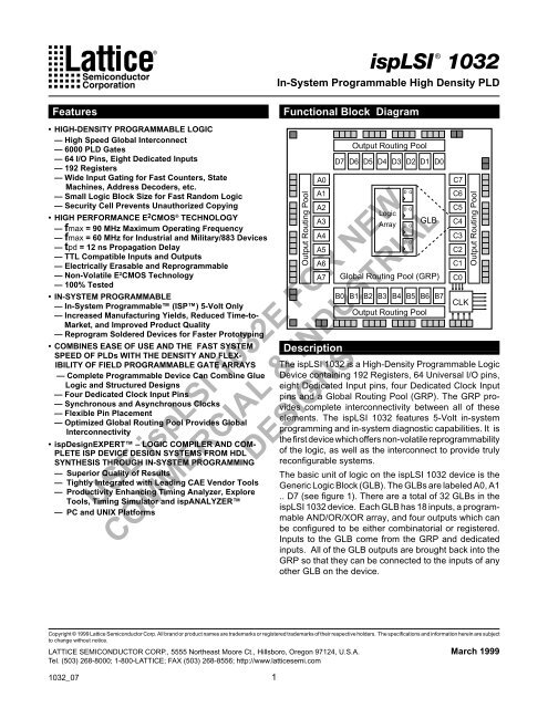
<strong>ispLSI</strong> ® <strong>1032</strong>In-System Programmable High Density PLDFeaturesFunctional Block Diagram• HIGH-DENSITY PROGRAMMABLE LOGIC— High Speed Global Interconnect— 6000 PLD Gates— 64 I/O Pins, Eight Dedicated Inputs— 192 Registers— Wide Input Gating for Fast Counters, StateMachines, Address Decoders, etc.— Small Logic Block Size for Fast Random Logic— Security Cell Prevents Unauthorized Copying• HIGH PERFORMANCE E 2 CMOS ® TECHNOLOGY— fmax = 90 MHz Maximum Operating Frequency— fmax = 60 MHz for Industrial and Military/883 Devices— tpd = 12 ns Propagation Delay— TTL Compatible Inputs and Outputs— Electrically Erasable and Reprogrammable— Non-Volatile E 2 CMOS Technology— 100% Tested• IN-SYSTEM PROGRAMMABLE— In-System Programmable (ISP) 5-Volt Only— Increased Manufacturing Yields, Reduced Time-to-Market, and Improved Product Quality— Reprogram Soldered Devices for Faster Prototyping• COMBINES EASE OF USE AND THE FAST SYSTEMSPEED OF PLDs WITH THE DENSITY AND FLEX-IBILITY OF FIELD PROGRAMMABLE GATE ARRAYS— Complete Programmable Device Can Combine GlueLogic and Structured Designs— Four Dedicated Clock Input Pins— Synchronous and Asynchronous Clocks— Flexible Pin Placement— Optimized Global Routing Pool Provides GlobalInterconnectivity• ispDesignEXPERT – LOGIC COMPILER AND COM-PLETE ISP DEVICE DESIGN SYSTEMS FROM HDLSYNTHESIS THROUGH IN-SYSTEM PROGRAMMING— Superior Quality of Results— Tightly Integrated with Leading CAE Vendor Tools— Productivity Enhancing Timing Analyzer, ExploreTools, Timing Simulator and ispANALYZER— PC and UNIX PlatformsOutput Routing PoolOutput Routing PoolD7 D6 D5 D4 D3 D2 D1 D0B0 B1 B2 B3 B4 B5 B6 B7Output Routing PoolUSE <strong>ispLSI</strong> <strong>1032</strong>E FOR NEWCOMMERCIAL & INDUSTRIALDESIGNSA0A1A2A3A4A5A6A7LogicArrayD QD QD QD QGLBGlobal Routing Pool (GRP)C7C6C5C4C3C2C1C0CLKOutput Routing PoolDescriptionThe <strong>ispLSI</strong> <strong>1032</strong> is a High-Density Programmable LogicDevice containing 192 Registers, 64 Universal I/O pins,eight Dedicated Input pins, four Dedicated Clock Inputpins and a Global Routing Pool (GRP). The GRP provides<strong>com</strong>plete interconnectivity between all of theseelements. The <strong>ispLSI</strong> <strong>1032</strong> features 5-Volt in-systemprogramming and in-system diagnostic capabilities. It isthe first device which offers non-volatile reprogrammabilityof the logic, as well as the interconnect to provide trulyreconfigurable systems.The basic unit of logic on the <strong>ispLSI</strong> <strong>1032</strong> device is theGeneric Logic Block (GLB). The GLBs are labeled A0, A1.. D7 (see figure 1). There are a total of 32 GLBs in the<strong>ispLSI</strong> <strong>1032</strong> device. Each GLB has 18 inputs, a programmableAND/OR/XOR array, and four outputs which canbe configured to be either <strong>com</strong>binatorial or registered.Inputs to the GLB <strong>com</strong>e from the GRP and dedicatedinputs. All of the GLB outputs are brought back into theGRP so that they can be connected to the inputs of anyother GLB on the device.Copyright © 1999 Lattice Semiconductor Corp. All brand or product names are trademarks or registered trademarks of their respective holders. The specifications and information herein are subjectto change without notice.LATTICE SEMICONDUCTOR CORP., 5555 Northeast Moore Ct., Hillsboro, Oregon 97124, U.S.A. March 1999Tel. (503) 268-8000; 1-800-LATTICE; FAX (503) 268-8556; http://www.latticesemi.<strong>com</strong><strong>1032</strong>_071
Specifications <strong>ispLSI</strong> <strong>1032</strong>Functional Block DiagramFigure 1. <strong>ispLSI</strong> <strong>1032</strong> Functional Block DiagramI/O I/O I/O I/O63 62 61 60I/O I/O I/O I/O59 58 57 56I/O I/O I/O I/O55 54 53 52I/O I/O I/O I/O51 50 49 48IN IN7 6RESETGenericLogic Blocks(GLBs)Input BusOutput Routing Pool (ORP)D7 D6 D5 D4 D3 D2 D1 D0IN 5IN 4I/O 0I/O 1I/O 2I/O 3I/O 4I/O 5I/O 6I/O 7I/O 8I/O 9I/O 10I/O 11I/O 12I/O 13I/O 14I/O 15Input BusOutput Routing Pool (ORP)A0A1A2A3A4A5A6A7GlobalRoutingPool(GRP)C7C6C5C4C3C2C1C0Output Routing Pool (ORP)lnput BusI/O 47I/O 46I/O 45I/O 44I/O 43I/O 42I/O 41I/O 40I/O 39I/O 38I/O 37I/O 36I/O 35I/O 34I/O 33I/O 32SDI/IN 0MODE/IN 1MegablockB0 B1 B2 B3 B4 B5 B6 B7Output Routing Pool (ORP)Input BusClockDistributionNetworkCLK 0CLK 1CLK 2IOCLK 0IOCLK 1ispENSDO/IN 2SCLK/IN 3I/O I/O I/O I/O16 17 18 19I/O20I/O I/O I/O21 22 23I/O24I/O I/O I/O25 26 27I/O I/O I/O I/O28 29 30 31Y0Y1Y2Y30139(1)-32-ispThe device also has 64 I/O cells, each of which is directlyconnected to an I/O pin. Each I/O cell can be individuallyprogrammed to be a <strong>com</strong>binatorial input, registered input,latched input, output or bi-directional I/O pin with3-state control. Additionally, all outputs are polarity selectable,active high or active low. The signal levels areTTL <strong>com</strong>patible voltages and the output drivers cansource 4 mA or sink 8 mA.Eight GLBs, 16 I/O cells, two dedicated inputs and oneORP are connected together to make a Megablock (seefigure 1). The outputs of the eight GLBs are connected toa set of 16 universal I/O cells by the ORP. The I/O cellswithin the Megablock also share a <strong>com</strong>mon OutputEnable (OE) signal. The <strong>ispLSI</strong> <strong>1032</strong> device contains fourof these Megablocks.The GRP has as its inputs the outputs from all of the GLBsand all of the inputs from the bi-directional I/O cells. All ofthese signals are made available to the inputs of theGLBs. Delays through the GRP have been equalized tominimize timing skew.Clocks in the <strong>ispLSI</strong> <strong>1032</strong> device are selected using theClock Distribution Network. Four dedicated clock pins(Y0, Y1, Y2 and Y3) are brought into the distributionnetwork, and five clock outputs (CLK 0, CLK 1, CLK 2,IOCLK 0 and IOCLK 1) are provided to route clocks to theGLBs and I/O cells. The Clock Distribution Network canalso be driven from a special clock GLB (C0 on the <strong>ispLSI</strong><strong>1032</strong> device). The logic of this GLB allows the user tocreate an internal clock from a <strong>com</strong>bination of internalsignals within the device.2
Specifications <strong>ispLSI</strong> <strong>1032</strong>Absolute Maximum Ratings 1Supply Voltage V cc .................................. -0.5 to +7.0VInput Voltage Applied........................ -2.5 to V CC +1.0VOff-State Output Voltage Applied ..... -2.5 to V CC +1.0VStorage Temperature................................ -65 to 150°CCase Temp. with Power Applied .............. -55 to 125°CMax. Junction Temp. (T J ) with Power Applied ... 150°C1. Stresses above those listed under the “Absolute Maximum Ratings” may cause permanent damage to the device. Functionaloperation of the device at these or at any other conditions above those indicated in the operational sections of this specificationis not implied (while programming, follow the programming specifications).DC Re<strong>com</strong>mended Operating ConditionsSYMBOL PARAMETERMIN. MAX. UNITSCommercialT A = 0°C to +70°C4.755.25VCCSupply VoltageIndustrialT A = -40°C to +85°C4.55.5VMilitary/883T C = -55°C to +125°C4.55.5VILInput Low Voltage00.8VVIHInput High Voltage2.0Vcc + 1VTable 2- 0005Aisp w/mil.epsCapacitance (T A =25 o C, f=1.0 MHz)SYMBOL PARAMETER MAXIMUM 1 UNITS TEST CONDITIONSC 1Dedicated Input CapacitanceCommercial/Industrial 8 pf V CC=5.0V, V IN=2.0VMilitary 10 pf V CC=5.0V, V IN=2.0VC 2I/O and Clock Capacitance 10 pf V CC=5.0V, V I/O, V Y=2.0V1. Guaranteed but not 100% tested.<strong>Data</strong> Retention SpecificationsTable 2- 0006<strong>Data</strong> RetentionErase/Reprogram CyclesPARAMETERMINIMUM MAXIMUM UNITS20—Years10000—CyclesTable 2- 0008B3
Specifications <strong>ispLSI</strong> <strong>1032</strong>Switching Test ConditionsInput Pulse Levels GND to 3.0VFigure 2. Test LoadInput Rise and Fall Time ≤ 3ns 10% to 90%Input Timing Reference Levels 1.5V+ 5VOutput Timing Reference Levels 1.5VR1Output Load See figure 23-state levels are measured 0.5V from steady-stateactive level.Table 2- 0003DeviceOutputR2CL*TestPointOutput Load Conditions (see figure 2)Test Condition R1 R2 CL*CL includes Test Fixture and Probe Capacitance.A 470Ω 390Ω 35pFB Active High 390Ω 35pFActive Low 470Ω 390Ω 35pFActive High to Z 390Ω 5pFC at V OH- 0.5V∞∞Active Low to Z 470Ω 390Ω 5pFat V OL+ 0.5VDC Electrical CharacteristicsOver Re<strong>com</strong>mended Operating ConditionsSYMBOLVOLVOHIILIIHIIL-ispIIL-PUIOS 1ICC 2,4PARAMETER CONDITION MIN. TYP. 3 MAX. UNITSOutput Low VoltageOutput High VoltageInput or I/O Low Leakage CurrentInput or I/O High Leakage Currentisp Input Low Leakage CurrentI/O Active Pull-Up CurrentOutput Short Circuit CurrentOperating Power Supply CurrentI OL =8 mAI OH =-4 mA0V ≤ V IN ≤ V IL (MAX.)3.5V ≤ V IN ≤ V CC0V ≤ V IN ≤ V IL (MAX.)0V ≤ V IN ≤ V ILV CC = 5V, V OUT = 0.5VV IL = 0.5V, V IH = 3.0V Commercialf TOGGLE = 1 MHz Industrial/MilitaryTable 2- 0007A-32-isp1. One output at a time for a maximum duration of one second.2. Measured using eight 16-bit counters.3. Typical values are at V CC= 5V and T A= 25 o C.4. Maximum I CCvaries widely with specific device configuration and operating frequency. Refer to the Power Consumption sectionof this datasheet and Thermal Management section of the Lattice Semiconductor <strong>Data</strong> Book or CD-ROM to estimate maximumI CC.–2.4––––––––––––––1301350.4–-1010-150-150-200190220VVµAµAµAµAmAmAmA4
Specifications <strong>ispLSI</strong> <strong>1032</strong>External Timing ParametersOver Re<strong>com</strong>mended Operating ConditionsPARAMETER TEST 5 # 2 DESCRIPTION 1-90 -80 -60UNITSCOND.MIN. MAX. MIN. MAX. MIN. MAX.tpd1tpd2fmax (Int.)AAA123<strong>Data</strong> Propagation Delay, 4PT bypass, ORP bypass<strong>Data</strong> Propagation Delay, Worst Case PathClock Frequency with Internal Feedback 3––90.91217–––801520–––602025–nsnsMHz1fmax (Ext.) – 4 Clock Frequency with External Feedback( MHztsu2 + tco1)58.8 – 50 – 38 –fmax (Tog.) – 5 Clock Frequency, Max Toggle 4125 – 100 – 83 – MHztsu1tco1th1tsu2tco2th2tr1trw1tentdistwhtwltsu5th5–A––––A–BC––––678910111213141516171819GLB Reg. Setup Time before Clock, 4PT bypassGLB Reg. Clock to Output Delay, ORP bypassGLB Reg. Hold Time after Clock, 4 PT bypassGLB Reg. Setup Time before ClockGLB Reg. Clock to Output DelayGLB Reg. Hold Time after ClockExt. Reset Pin to Output DelayExt. Reset Pulse DurationInput to Output EnableInput to Output DisableExt. Sync. Clock Pulse Duration, HighExt. Sync. Clock Pulse Duration, LowI/O Reg. Setup Time before Ext. Sync. Clock (Y2, Y3)I/O Reg. Hold Time after Ext. Sync. Clock (Y2, Y3)6–09–0–10––4426.5–8––10–15–1515––––7–010–0–10––5526.5–10––12–17–1818––––9–013–0–13––662.58.5–13––16–22.5–2424––––nsnsnsnsnsnsnsnsnsnsnsnsnsnsUSE <strong>1032</strong>E-100FOR NEW DESIGNS1. Unless noted otherwise, all parameters use a GRP load of 4 GLBs, 20 PTXOR path, ORP and Y0 clock.2. Refer to Timing Model in this data sheet for further details.3. Standard 16-Bit counter using GRP feedback.4. fmax (Toggle) may be less than 1/(twh + twl). This is to allow for a clock duty cycle of other than 50%.5. Reference Switching Test Conditions section.USE <strong>1032</strong>E-70FOR NEW DESIGNSUSE <strong>1032</strong>E-70FOR NEW DESIGNSTable 2-0030-32/90,80,60C5
Specifications <strong>ispLSI</strong> <strong>1032</strong>Internal Timing Parameters 1PARAMETERInputstiobptiolattiosutiohtiocotiortdinGRPtgrp1tgrp4tgrp8tgrp12tgrp16tgrp32GLBt4ptbpt1ptxort20ptxortxoradjtgbptgsutghtgcotgrtptretptoetptckORP# 220212223242526272829303132333435363738394041424344DESCRIPTIONI/O Register BypassI/O Latch DelayI/O Register Setup Time before ClockI/O Register Hold Time after ClockI/O Register Clock to Out DelayI/O Register Reset to Out DelayDedicated Input DelayGRP Delay, 1 GLB LoadGRP Delay, 4 GLB LoadsGRP Delay, 8 GLB LoadsGRP Delay, 12 GLB LoadsGRP Delay, 16 GLB LoadsGRP Delay, 32 GLB Loads4 Product Term Bypass Path Delay1 Product Term/XOR Path Delay20 Product Term/XOR Path DelayXOR Adjacent Path Delay 3GLB Register Bypass DelayGLB Register Setup Time before ClockGLB Register Hold Time after ClockGLB Register Clock to Output DelayGLB Register Reset to Output DelayGLB Product Term Reset to Register DelayGLB Product Term Output Enable to I/O Cell DelayGLB Product Term Clock Delaytorp 45 ORP Delaytorpbp 46 ORP Bypass Delay1. Internal Timing Parameters are not tested and are for reference only.2. Refer to Timing Model in this data sheet for further details.3. The XOR adjacent path can only be used by hard macros.-90MIN. MAX.– 1.6– 2.44.8USE <strong>1032</strong>E-100 FOR NEW DESIGNS2.1––––––––––––––1.23.6––––2.8––––2.42.83.21.21.62.43.03.66.45.25.77.08.20.8––1.62.08.07.86.02.40.4-80 -60UNITSMIN. MAX. MIN. MAX.––5.51.0––––––––––––––1.04.5––––3.5––2.03.0––3.02.54.01.52.03.03.84.58.06.57.08.09.51.0––2.02.510.09.07.52.50.5––7.31.3––––––––––––––1.36.0––––4.6––2.74.0––4.03.35.32.02.74.05.06.010.68.69.310.612.71.3––2.73.313.312.09.93.30.7nsnsnsnsnsnsnsnsnsnsnsnsnsnsnsnsnsnsnsnsnsnsnsnsnsnsnsUSE <strong>1032</strong>E-70 FOR NEW DESIGNSUSE <strong>1032</strong>E-70 FOR NEW DESIGNS6
Specifications <strong>ispLSI</strong> <strong>1032</strong>Internal Timing Parameters 1# 2 PARAMETER DESCRIPTION-90 -80 -60UNITSMIN. MAX. MIN. MAX. MIN. MAX.Outputstobtoentodis474849Output Buffer DelayI/O Cell OE to Output EnabledI/O Cell OE to Output Disabled–––2.44.04.0–––3.05.05.0–––4.06.76.7nsnsnsClockstgy0tgy1/2tgcptioy2/3tiocpGlobal Resettgr505152535455Clock Delay, Y0 to Global GLB Clock Line (Ref. clock)Clock Delay, Y1 or Y2 to Global GLB Clock LineClock Delay, Clock GLB to Global GLB Clock LineClock Delay, Y2 or Y3 to I/O Cell Global Clock LineClock Delay, Clock GLB to I/O Cell Global Clock LineGlobal Reset to GLB and I/O Registers1. Internal Timing Parameters are not tested and are for reference only.2. Refer to Timing Model in this data sheet for further details.USE <strong>1032</strong>E-100FOR NEW DESIGNS3.62.80.82.80.8–3.64.44.04.44.08.2USE <strong>1032</strong>E-70FOR NEW DESIGNS4.53.51.03.51.0–4.55.55.05.55.09.0USE <strong>1032</strong>E-70FOR NEW DESIGNS6.04.61.34.61.3–6.07.36.67.36.612.0nsnsnsnsnsns7
Specifications <strong>ispLSI</strong> <strong>1032</strong><strong>ispLSI</strong> <strong>1032</strong> Timing ModelI/O CellGRPGLBORPI/O CellFeedbackDed. InI/O Pin(Input)Reset#55#26I/O Reg Bypass#20InputGRPD Register QLoadingDelayRST#21 - 25 #27, 29,30, 31, 32GRP 4 4 PT Bypass GLB Reg Bypass ORP Bypass#28 #3320 PTXOR Delays#34, 35, 36#55#37GLB RegDelayD QRST#38, 39,40, 41#46ORPDelay#45#47I/O Pin(Output)#48, 49Y1,2,3ClockDistribution#51, 52,53, 54ControlPTs#42, 43,44REOECKY0#50Derivations of tsu, th and tco from the Product Term Clock 1tsu= Logic + Reg su - Clock (min)= (tiobp + tgrp4 + t20ptxor) + (tgsu) - (tiobp + tgrp4 + tptck(min))= (#20 + #28 + #35) + (#38) - (#20 + #28 + #44)5.5 ns = (2.0 + 2.0 + 8.0) + (1.0) - (2.0 + 2.0 + 3.5)th= Clock (max) + Reg h - Logic= (tiobp + tgrp4 + tptck(max)) + (tgh) - (tiobp + tgrp4 + t20ptxor)= (#20 + #28 + #44) + (#39) - (#20 + #28 + #35)4.0 ns = (2.0 + 2.0 + 7.5) + (4.5) - (2.0 + 2.0 + 8.0)tco = Clock (max) + Reg co + Output= (tiobp + tgrp4 + tptck(max)) + (tgco) + (torp + tob)= (#20 + #28 + #44) + (#40) + (#45 + #47)19.0 ns = (2.0+ 2.0 +7.5) + (2.0) + (2.5 + 3.0)Derivations of tsu, th and tco from the Clock GLB 1tsu= Logic + Reg su - Clock (min)= (tiobp + tgrp4 + t20ptxor) + (tgsu) - (tgy0(min) + tgco + tgcp(min))= (#20 + #28 + #35) + (#38) - (#50 + #40 + #52)5.5 ns = (2.0 + 2.0 + 8.0) + (1.0) - (4.5 + 2.0 + 1.0)th= Clock (max) + Reg h - Logic= (tgy0(max) + tgco + tgcp(max)) + (tgh) - (tiobp + tgrp4 + t20ptxor)= (#50 + #40 + #52) + (#39) - (#20 + #28 + #35)4.0 ns = (4.5 + 2.0 + 5.0) + (4.5) - (2.0 + 2.0 + 8.0)tco = Clock (max) + Reg co + Output= (tgy0(max) + tgco + tgcp(max)) + (tgco) + (torp + tob)= (#50 + #40 + #52) + (#40) + (#45 + #47)19.0 ns = (4.5 + 2.0 + 5.0) + (2.0) + (2.5 + 3.0)1. Calculations are based upon timing specifications for the <strong>ispLSI</strong> <strong>1032</strong>-80.8
Specifications <strong>ispLSI</strong> <strong>1032</strong>Maximum GRP Delay vs GLB LoadsGRP Delay (ns)654321<strong>ispLSI</strong> <strong>1032</strong>-60<strong>ispLSI</strong> <strong>1032</strong>-80<strong>ispLSI</strong> <strong>1032</strong>-9004 8 12 16GLB Loads0126A-80-32-ispPower ConsumptionPower consumption in the <strong>ispLSI</strong> <strong>1032</strong> device dependson two primary factors: the speed at which the device isoperating, and the number of Product Terms used. Fig-ure 3 shows the relationship between power and operatingspeed.Figure 3. Typical Device Power Consumption vs fmaxICC (mA)250200150100<strong>ispLSI</strong> <strong>1032</strong>500 10 20 30 40 50 60 70fmax (MHz)80Notes: Configuration of eight 16-bit CountersTypical Current at 5V, 25ßCICC can be estimated for the <strong>ispLSI</strong> <strong>1032</strong> using the following equation:ICC = 52 + (# of PTs * 0.30) + (# of nets * Max. freq * 0.009) where:# of PTs = Number of Product Terms used in design# of nets = Number of Signals used in deviceMax. freq = Highest Clock Frequency to the deviceThe ICC estimate is based on typical conditions (VCC = 5.0V, room temperature) and an assumption of 2 GLB loads onaverage exists. These values are for estimates only. Since the value of ICC is sensitive to operating conditions and theprogram in the device, the actual ICC should be verified.0127A-32-80-isp9
Specifications <strong>ispLSI</strong> <strong>1032</strong>Pin DescriptionName PLCC Pin Numbers DescriptionI/O 0 - I/O 3 26, 27, 28, 29,I/O 4 - I/O 7 30, 31, 32, 33,I/O 8 - I/O 11 34, 35, 36, 37,I/O 12 - I/O 15 38, 39, 40, 41,I/O 16 - I/O 19 45, 46, 47, 48,I/O 20 - I/O 23 49, 50, 51, 52,I/O 24 - I/O 27 53, 54, 55, 56,I/O 28 - I/O 31 57, 58, 59, 60,I/O 32 - I/O 35 68, 69, 70, 71,I/O 36 - I/O 39 72, 73, 74, 75,I/O 40 - I/O 43 76, 77, 78, 79,I/O 44 - I/O 47 80, 81, 82, 83,I/O 48 - I/O 51 3, 4, 5, 6,I/O 52 - I/O 55 7, 8, 9, 10,I/O 56 - I/O 59 11, 12, 13, 14,I/O 60 - I/O 63 15, 16, 17, 18Input/Output Pins - These are the general purpose I/O pins used by thelogic array.IN 4 - IN 7 67, 84, 2, 19 Dedicated input pins to the device.ispEN 23SDI/IN 0 1 25MODE/IN 1 1 42SDO/IN 2 1 44SCLK/IN 3 1 61RESET 24Y0 20Y1 66Y2 63Y3 62GND 1, 22, 43, 64VCC 21, 65Input — Dedicated in-system programming enable input pin. This pinis brought low to enable the programming mode. The MODE, SDI,SDO and SCLK options be<strong>com</strong>e active.Input — This pin performs two functions. It is a dedicated input pin whenispEN is logic high. When ispEN is logic low, it functions as an inputpin to load programming data into the device. SDI/IN 0 also is used asone of the two control pins for the isp state machine.Input — This pin performs two functions. It is a dedicated input pin whenispEN is logic high. When ispEN is logic low, it functions as a pin tocontrol the operation of the isp state machine.Input/Output — This pin performs two functions. It is a dedicated inputpin when ispEN is logic high. When ispEN is logic low, it functions asan output pin to read serial shift register data.Input — This pin performs two functions. It is a dedicated input whenispEN is logic high. When ispEN is logic low, it functions as a clock pinfor the Serial Shift Register.Active Low (0) Reset pin which resets all of the GLB and I/O registersin the device.Dedicated Clock input. This clock input is connected to one of theclock inputs of all of the GLBs on the device.Dedicated Clock input. This clock input is brought into the clockdistribution network, and can optionally be routed to any GLB on thedevice.Dedicated Clock input. This clock input is brought into the clockdistribution network, and can optionally be routed to any GLB and/orany I/O cell on the device.Dedicated Clock input. This clock input is brought into the clockdistribution network, and can optionally be routed to any I/O cell on thedevice.Ground (GND)V CC1. Pins have dual function capability10
Specifications <strong>ispLSI</strong> <strong>1032</strong>Pin DescriptionNameTQFP Pin NumbersDescriptionI/O 0 - I/O 3 17, 18, 19, 20, Input/Output Pins - These are the general purpose I/O pins used by theI/O 4 - I/O 7 21, 22, 23, 28, logic array.I/O 8 - I/O 11 29, 30, 31, 32,I/O 12 - I/O 15 33, 34, 35, 36,I/O 16 - I/O 19 40, 41, 42, 43,I/O 20 - I/O 23 44, 45, 46, 47,I/O 24 - I/O 27 48, 53, 54, 55,I/O 28 - I/O 31 56, 57, 58, 59,I/O 32 - I/O 35 67, 68, 69, 70,I/O 36 - I/O 39 71, 72, 73, 78,I/O 40 - I/O 43 79, 80, 81, 82,I/O 44 - I/O 47 83, 84, 85, 86,I/O 48 - I/O 51 90, 91, 92, 93,I/O 52 - I/O 55 94, 95, 96, 97,I/O 56 - I/O 59 98, 3, 4, 5,I/O 60 - I/O 63 6, 7, 8, 9IN 4 - IN 7 66, 87, 89, 10 Dedicated input pins to the device.ispEN 14SDI/IN 0 1 16MODE/IN 1 1 37SDO/IN 2 1 39SCLK/IN 3 1 60NC 2 1, 2, 24, 25,26, 27, 49, 50,51, 52, 74, 7576, 77, 99, 100RESET 15Y0 11Y1 65Y2 62Y3 61GND 13, 38, 63, 88VCC 12, 64Input — Dedicated in-system programming enable input pin. This pinis brought low to enable the programming mode. The MODE, SDI,SDO and SCLK options be<strong>com</strong>e active.Input — This pin performs two functions. It is a dedicated input pin whenispEN is logic high. When ispEN is logic low, it functions as an inputpin to load programming data into the device. SDI/IN 0 also is used asone of the two control pins for the isp state machine.Input — This pin performs two functions. It is a dedicated input pin whenispEN is logic high. When ispEN is logic low, it functions as a pin tocontrol the operation of the isp state machine.Input/Output — This pin performs two functions. It is a dedicated inputpin when ispEN is logic high. When ispEN is logic low, it functions asan output pin to read serial shift register data.Input — This pin performs two functions. It is a dedicated input whenispEN is logic high. When ispEN is logic low, it functions as a clock pinfor the Serial Shift Register.No ConnectActive Low (0) Reset pin which resets all of the GLB and I/O registersin the device.Dedicated Clock input. This clock input is connected to one of theclock inputs of all of the GLBs on the device.Dedicated Clock input. This clock input is brought into the clockdistribution network, and can optionally be routed to any GLB on thedevice.Dedicated Clock input. This clock input is brought into the clockdistribution network, and can optionally be routed to any GLB and/orany I/O cell on the device.Dedicated Clock input. This clock input is brought into the clockdistribution network, and can optionally be routed to any I/O cell on thedevice.Ground (GND)V CC1. Pins have dual function capability2. NC pins are not to be connected to any active signals, Vcc or GND.11
Specifications <strong>ispLSI</strong> <strong>1032</strong>Pin DescriptionName CPGA Pin Numbers DescriptionI/O 0 - I/O 3 F1, H1, H2, J1,I/O 4 - I/O 7 K1, J2, L1, K2,I/O 8 - I/O 11 K3, L2, L3, K4,I/O 12 - I/O 15 L4, J5, K5, L5,I/O 16 - I/O 19 L7, K7, L6, L8,I/O 20 - I/O 23 K8, L9, L10, K9,I/O 24 - I/O 27 L11, K10, J10, K11,I/O 28 - I/O 31 J11, H10, H11, F10,I/O 32 - I/O 35 E9, D11, D10, C11,I/O 36 - I/O 39 B11, C10, A11, B10,I/O 40 - I/O 43 B9, A10, A9, B8,I/O 44 - I/O 47 A8, B6, B7, A7,I/O 48 - I/O 51 A5, B5, C5, A4,I/O 52 - I/O 55 B4, A3, A2, B3,I/O 56 - I/O 59 A1, B2, C2, B1,I/O 60 - I/O 63 C1, D2, D1, E3Input/Output Pins - These are the general purpose I/O pins used by thelogic array.IN 4 - IN 7 E10, C7, A6, E2 Dedicated input pins to the device.ispENSDI/IN 0 1MODE/IN 1 1SDO/IN 2 1SCLK/IN 3 1RESETY0Y1Y2Y3NC 2G3G2K6J7G10G1E1E11G9G11G3Input – Dedicated in-system programming enable input pin. This pinis brought low to enable the programming mode. The MODE, SDI,SDO and SCLK options be<strong>com</strong>e active.Input – This pin performs two functions. It is a dedicated input pin whenispEN is logic high. When ispEN is logic low, it functions as an inputpin to load programming data into the device. SDI/IN 0 also is used asone of the two control pins for the isp state machine.Input – This pin performs two functions. It is a dedicated input pin whenispEN is logic high. When ispEN is logic low, it functions as a pin tocontrol the operation of the isp state machine.Input/Output – This pin performs two functions. It is a dedicated inputpin when ispEN is logic high. When ispEN is logic low, it functions asan output pin to read serial shift register data.Input – This pin performs two functions. It is a dedicated input whenispEN is logic high. When ispEN is logic low, it functions as a clock pinfor the Serial Shift Register.Active Low (0) Reset pin which resets all of the GLB and I/O registersin the device.Dedicated Clock input. This clock input is connected to one of theclock inputs of all of the GLBs on the device.Dedicated Clock input. This clock input is brought into the clockdistribution network, and can optionally be routed to any GLB on thedevice.Dedicated Clock input. This clock input is brought into the clockdistribution network, and can optionally be routed to any GLB and/orany I/O cell on the device.Dedicated Clock input. This clock input is brought into the clockdistribution network, and can optionally be routed to any I/O cell on thedevice.No ConnectGND C6, F3, F9, J6VCC F2, F11Ground (GND)V CCTable 2-0002-32/8831. Pins have dual function capability.2. NC pins are not to be connected to any active signals, Vcc or GND.12
Specifications <strong>ispLSI</strong> <strong>1032</strong>Pin Configuration<strong>ispLSI</strong> <strong>1032</strong> 84-Pin PLCC Pinout DiagramI/O 56I/O 55I/O 54I/O 53I/O 52I/O 51I/O 50I/O 49I/O 48IN 6GNDIN 5I/O 47I/O 46I/O 45I/O 44I/O 43I/O 42I/O 41I/O 40I/O 3911 10 9 8 7 6 5 4 3 2 1 84 83 82 81 80 79 78 77 76 75I/O 571274I/O 38I/O 58I/O 59I/O 60I/O 611314151673727170I/O 37I/O 36I/O 35I/O 34I/O 621769I/O 33I/O 631868I/O 32IN 71967IN 4Y02066Y1VCCGNDispENRESET21222324<strong>ispLSI</strong> <strong>1032</strong>Top View65646362VCCGNDY2Y3*SDI/IN 02561IN 3/SCLK*I/O 0I/O 1I/O 2262728605958I/O 31I/O 30I/O 29I/O 32957I/O 28I/O 4I/O 5I/O 6303132565554I/O 27I/O 26I/O 2533 34 35 36 37 38 39 40 41 42 43 44 45 46 47 48 49 50 51 52 53I/O 7I/O 8I/O 9I/O 10I/O 11I/O 12I/O 13I/O 14I/O 15*MODE/IN 1GND*SDO/IN 2I/O 16I/O 17I/O 18I/O 19I/O 20I/O 21I/O 22I/O 23I/O 24*Pins have dual function capability.0123-32-isp13
Specifications <strong>ispLSI</strong> <strong>1032</strong>Pin Configuration<strong>ispLSI</strong> <strong>1032</strong> 100-pin TQFP Pinout DiagramNC 1NC 1I/O 56I/O 55I/O 54I/O 53I/O 52I/O 51I/O 50I/O 49I/O 48IN 6GNDIN 5I/O 47I/O 46I/O 45I/O 44I/O 43I/O 42I/O 41I/O 40I/O 39NC 1NC 11 NC1 NCI/O 57I/O 58I/O 59I/O 60I/O 61I/O 62I/O 63IN 7Y0VCCGNDispENRESET2 SDI/IN 0I/O 0I/O 1I/O 2I/O 3I/O 4I/O 5I/O 61 NC100999897969594939291908988878685848382818079787776175 NC 1274373472571670769868967106611 <strong>ispLSI</strong> <strong>1032</strong>65126413Top View631462156116601759185819572056215522542353NC 11 2452NC 2551 NC 1NC 1I/O 38I/O 37I/O 36I/O 35I/O 34I/O 33I/O 32IN 4Y1VCCGNDY2Y3IN 3/SCLK 2I/O 31I/O 30I/O 29I/O 28I/O 27I/O 26I/O 251 NC1 NCI/O 7I/O 8I/O 9I/O 10I/O 11I/O 12I/O 13I/O 14I/O 152 MODE/IN1GND2 SDO/IN 2I/O 16I/O 17I/O 18I/O 19I/O 20I/O 21I/O 22I/O 23I/O 241 NC1 NC262728293031323334353637383940414243444546474849501. NC pins are not to be connected to any active signal, Vcc or GND.2. Pins have dual function capability.0766A-32-isp14
Specifications <strong>ispLSI</strong> <strong>1032</strong>Pin Configuration<strong>ispLSI</strong> <strong>1032</strong>/883 84-Pin CPGA Pinout Diagram11 10 9 8 7 6 5 4 3 2 1 PIN A1I/O38I/O41I/O42I/O44I/O47IN6I/O48I/O51I/O53I/O54I/O56AI/O36I/O39I/O40I/O43I/O46I/O45I/O49I/O52I/O55I/O57I/O59BI/O35I/O37IN5GNDI/O50INDEXI/O58I/O60CI/O33I/O34I/O61I/O62DY1IN4I/O32I/O63IN7Y0EVccI/O31GND<strong>ispLSI</strong> <strong>1032</strong>/883Bottom ViewGNDVccI/O0FY3*SCLK/IN3Y2ispEN*SDI/IN0RESETGI/O30I/O29I/O2I/O1HI/O28I/O26*SDO/IN2GNDI/O13I/O5I/O3JI/O27I/O25I/O23I/O20I/O17*MODE/IN1I/O14I/O11I/O8I/O7I/O4KI/O24I/O22I/O21I/O19I/O16I/O18I/O15I/O12I/O10I/O9I/O6L*Pins have dual function capability.0488A-32-isp/88315
Specifications <strong>ispLSI</strong> <strong>1032</strong>Part Number Description<strong>ispLSI</strong><strong>1032</strong> — XX X X XDevice FamilyDevice NumberSpeed90 = 90 MHz fmax80 = 80 MHz fmax60 = 60 MHz fmaxGradeBlank = CommercialI = Industrial/883 = 883 Military ProcessPackageJ = PLCCT = TQFPG = CPGAPowerL = Low0212-80B-isp<strong>1032</strong>Ordering InformationFamily<strong>ispLSI</strong>Family<strong>ispLSI</strong>Family<strong>ispLSI</strong>COMMERCIALfmax (MHz) tpd (ns) Ordering Number Package90 12 <strong>ispLSI</strong> <strong>1032</strong>-90LJ 84-Pin PLCC90 12 <strong>ispLSI</strong> <strong>1032</strong>-90LT 100-Pin TQFP80 15 <strong>ispLSI</strong> <strong>1032</strong>-80LJ 84-Pin PLCC80 15 <strong>ispLSI</strong> <strong>1032</strong>-80LT 100-Pin TQFP60 20 <strong>ispLSI</strong> <strong>1032</strong>-60LJ 84-Pin PLCC60 20 <strong>ispLSI</strong> <strong>1032</strong>-60LT 100-Pin TQFPINDUSTRIALfmax (MHz) tpd (ns) Ordering Number Package60 20 <strong>ispLSI</strong> <strong>1032</strong>-60LJI 84-Pin PLCC60 20 <strong>ispLSI</strong> <strong>1032</strong>-60LTI 100-Pin TQFPMILITARY/883fmax (MHz) tpd (ns) Ordering Number SMD Number Package60 20 <strong>ispLSI</strong> <strong>1032</strong>-60LG/883 5962-9308501MXC 84-Pin CPGANote: Lattice Semiconductor recognizes the trend in military device procurement towardsusing SMD <strong>com</strong>pliant devices, as such, ordering by this number is re<strong>com</strong>mended.USE <strong>ispLSI</strong> <strong>1032</strong>EFOR NEW COMMERCIAL &INDUSTRIAL DESIGNSTable 2- 0041A-32-isp16