27C512 EPROM Data Sheet.pdf - Downloads.reactivemicro.com
27C512 EPROM Data Sheet.pdf - Downloads.reactivemicro.com
27C512 EPROM Data Sheet.pdf - Downloads.reactivemicro.com

Create successful ePaper yourself
Turn your PDF publications into a flip-book with our unique Google optimized e-Paper software.
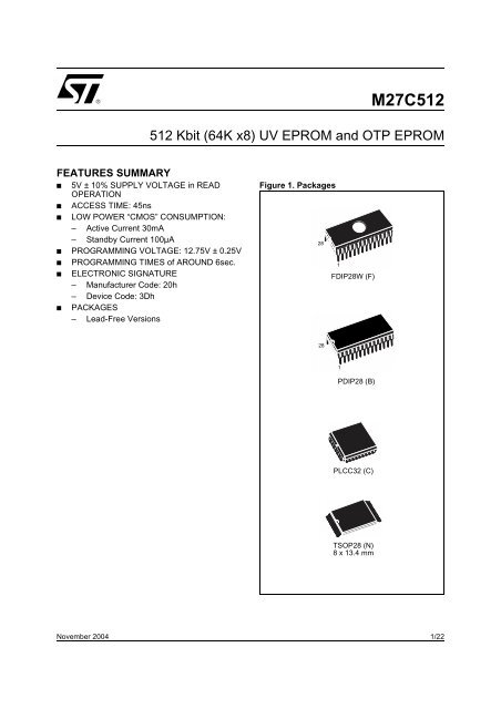
M<strong>27C512</strong>512 Kbit (64K x8) UV <strong>EPROM</strong> and OTP <strong>EPROM</strong>FEATURES SUMMARY■ 5V ± 10% SUPPLY VOLTAGE in READOPERATION■ ACCESS TIME: 45ns■ LOW POWER “CMOS” CONSUMPTION:– Active Current 30mA– Standby Current 100µA■ PROGRAMMING VOLTAGE: 12.75V ± 0.25V■ PROGRAMMING TIMES of AROUND 6sec.■ ELECTRONIC SIGNATURE– Manufacturer Code: 20h– Device Code: 3Dh■ PACKAGES– Lead-Free VersionsFigure 1. Packages281FDIP28W (F)281PDIP28 (B)PLCC32 (C)TSOP28 (N)8 x 13.4 mmNovember 20041/22
M<strong>27C512</strong>TABLE OF CONTENTSFEATURES SUMMARY . . . . . . . . . . . . . . . . . . . . . . . . . . . . . . . . . . . . . . . . . . . . . . . . . . . . . . . . . . . . . 1Figure 1. Packages . . . . . . . . . . . . . . . . . . . . . . . . . . . . . . . . . . . . . . . . . . . . . . . . . . . . . . . . . . . . . . 1SUMMARY DESCRIPTION. . . . . . . . . . . . . . . . . . . . . . . . . . . . . . . . . . . . . . . . . . . . . . . . . . . . . . . . . . . 4Figure 2. Logic Diagram . . . . . . . . . . . . . . . . . . . . . . . . . . . . . . . . . . . . . . . . . . . . . . . . . . . . . . . . . . 4Table 1. Signal Names . . . . . . . . . . . . . . . . . . . . . . . . . . . . . . . . . . . . . . . . . . . . . . . . . . . . . . . . . . 4Figure 3. DIP Connections . . . . . . . . . . . . . . . . . . . . . . . . . . . . . . . . . . . . . . . . . . . . . . . . . . . . . . . . 5Figure 4. LCC Connections. . . . . . . . . . . . . . . . . . . . . . . . . . . . . . . . . . . . . . . . . . . . . . . . . . . . . . . . 5Figure 5. TSOP Connections . . . . . . . . . . . . . . . . . . . . . . . . . . . . . . . . . . . . . . . . . . . . . . . . . . . . . . 5DEVICE OPERATION . . . . . . . . . . . . . . . . . . . . . . . . . . . . . . . . . . . . . . . . . . . . . . . . . . . . . . . . . . . . . . . 6Read Mode . . . . . . . . . . . . . . . . . . . . . . . . . . . . . . . . . . . . . . . . . . . . . . . . . . . . . . . . . . . . . . . . . . . . 6Standby Mode . . . . . . . . . . . . . . . . . . . . . . . . . . . . . . . . . . . . . . . . . . . . . . . . . . . . . . . . . . . . . . . . . 6Table 2. Operating Modes . . . . . . . . . . . . . . . . . . . . . . . . . . . . . . . . . . . . . . . . . . . . . . . . . . . . . . . . 6Table 3. Electronic Signature. . . . . . . . . . . . . . . . . . . . . . . . . . . . . . . . . . . . . . . . . . . . . . . . . . . . . . 6Two Line Output Control . . . . . . . . . . . . . . . . . . . . . . . . . . . . . . . . . . . . . . . . . . . . . . . . . . . . . . . . 6System Considerations. . . . . . . . . . . . . . . . . . . . . . . . . . . . . . . . . . . . . . . . . . . . . . . . . . . . . . . . . . 6Programming . . . . . . . . . . . . . . . . . . . . . . . . . . . . . . . . . . . . . . . . . . . . . . . . . . . . . . . . . . . . . . . . . . 7Figure 6. Programming Flowchart. . . . . . . . . . . . . . . . . . . . . . . . . . . . . . . . . . . . . . . . . . . . . . . . . . . 7PRESTO IIB Programming Algorithm . . . . . . . . . . . . . . . . . . . . . . . . . . . . . . . . . . . . . . . . . . . . . . 7Program Inhibit . . . . . . . . . . . . . . . . . . . . . . . . . . . . . . . . . . . . . . . . . . . . . . . . . . . . . . . . . . . . . . . . 7Program Verify. . . . . . . . . . . . . . . . . . . . . . . . . . . . . . . . . . . . . . . . . . . . . . . . . . . . . . . . . . . . . . . . . 7Electronic Signature . . . . . . . . . . . . . . . . . . . . . . . . . . . . . . . . . . . . . . . . . . . . . . . . . . . . . . . . . . . . 7ERASURE OPERATION (APPLIES FOR UV <strong>EPROM</strong>) . . . . . . . . . . . . . . . . . . . . . . . . . . . . . . . . . . . . . 8MAXIMUM RATING. . . . . . . . . . . . . . . . . . . . . . . . . . . . . . . . . . . . . . . . . . . . . . . . . . . . . . . . . . . . . . . . . 9Table 4. Absolute Maximum Ratings . . . . . . . . . . . . . . . . . . . . . . . . . . . . . . . . . . . . . . . . . . . . . . . . 9DC and AC PARAMETERS . . . . . . . . . . . . . . . . . . . . . . . . . . . . . . . . . . . . . . . . . . . . . . . . . . . . . . . . . 10Table 5. AC Measurement Conditions. . . . . . . . . . . . . . . . . . . . . . . . . . . . . . . . . . . . . . . . . . . . . . 10Figure 7. Testing Input Output Waveform. . . . . . . . . . . . . . . . . . . . . . . . . . . . . . . . . . . . . . . . . . . . 10Figure 8. AC Testing Load Circuit. . . . . . . . . . . . . . . . . . . . . . . . . . . . . . . . . . . . . . . . . . . . . . . . . . 10Table 6. Capacitance. . . . . . . . . . . . . . . . . . . . . . . . . . . . . . . . . . . . . . . . . . . . . . . . . . . . . . . . . . . 10Table 7. Read Mode DC Characteristics . . . . . . . . . . . . . . . . . . . . . . . . . . . . . . . . . . . . . . . . . . . . 11Table 8. Read Mode AC Characteristics . . . . . . . . . . . . . . . . . . . . . . . . . . . . . . . . . . . . . . . . . . . . 11Table 9. Read Mode AC Characteristics . . . . . . . . . . . . . . . . . . . . . . . . . . . . . . . . . . . . . . . . . . . . 12Figure 9. Read Mode AC Waveforms . . . . . . . . . . . . . . . . . . . . . . . . . . . . . . . . . . . . . . . . . . . . . . . 12Table 10. Programming Mode DC Characteristics . . . . . . . . . . . . . . . . . . . . . . . . . . . . . . . . . . . . . 13Table 11. Margin Mode AC Characteristics . . . . . . . . . . . . . . . . . . . . . . . . . . . . . . . . . . . . . . . . . . . 14Figure 10.Margin Mode AC Waveforms . . . . . . . . . . . . . . . . . . . . . . . . . . . . . . . . . . . . . . . . . . . . . 14Table 12. Programming Mode AC Characteristics . . . . . . . . . . . . . . . . . . . . . . . . . . . . . . . . . . . . . 15Figure 11.Programming and Verify Modes AC Waveforms. . . . . . . . . . . . . . . . . . . . . . . . . . . . . . . 152/22
M<strong>27C512</strong>PACKAGE MECHANICAL . . . . . . . . . . . . . . . . . . . . . . . . . . . . . . . . . . . . . . . . . . . . . . . . . . . . . . . . . . 16Figure 12.FDIP28W - 28 pin Ceramic Frit-seal DIP, with window, Package Outline. . . . . . . . . . . . 16Table 13. FDIP28W - 28 pin Ceramic Frit-seal DIP, with window, Package Mechanical <strong>Data</strong> . . . . 16Figure 13.PDIP28 - 28 pin Plastic DIP, 600 mils width, Package Outline . . . . . . . . . . . . . . . . . . . . 17Table 14. PDIP28 - 28 pin Plastic DIP, 600 mils width, Package Mechanical <strong>Data</strong> . . . . . . . . . . . . 17Figure 14.PLCC32 - 32 lead Plastic Leaded Chip Carrier, Package Outline . . . . . . . . . . . . . . . . . 18Table 15. PLCC32 - 32 lead Plastic Leaded Chip Carrier, Package Mechanical <strong>Data</strong> . . . . . . . . . . 18Figure 15.TSOP28 - 28 lead Plastic Thin Small Outline, 8 x 13.4 mm, Package Outline . . . . . . . . 19Table 16. TSOP28 - 28 lead Plastic Thin Small Outline, 8 x 13.4 mm, Package Mechanical <strong>Data</strong> 19PART NUMBERING . . . . . . . . . . . . . . . . . . . . . . . . . . . . . . . . . . . . . . . . . . . . . . . . . . . . . . . . . . . . . . . 20Table 17. Ordering Information Scheme . . . . . . . . . . . . . . . . . . . . . . . . . . . . . . . . . . . . . . . . . . . . . 20REVISION HISTORY. . . . . . . . . . . . . . . . . . . . . . . . . . . . . . . . . . . . . . . . . . . . . . . . . . . . . . . . . . . . . . . 21Table 18. Revision History. . . . . . . . . . . . . . . . . . . . . . . . . . . . . . . . . . . . . . . . . . . . . . . . . . . . . . . . 213/22
M<strong>27C512</strong>SUMMARY DESCRIPTIONThe M<strong>27C512</strong> is a 512 Kbit <strong>EPROM</strong> offered in thetwo ranges UV (ultra violet erase) and OTP (onetime programmable). It is ideally suited for applicationswhere fast turn-around and pattern experimentationare important requirements and isorganized as 65536 by 8 bits.The FDIP28W (window ceramic frit-seal package)has transparent lid which allows the user to exposethe chip to ultraviolet light to erase the bit pattern.A new pattern can then be written to thedevice by following the programming procedure.For applications where the content is programmedonly one time and erasure is not required, theM<strong>27C512</strong> is offered in PDIP28, PLCC32 andTSOP28 (8 x 13.4 mm) packages.In addition to the standard versions, the packagesare also available in Lead-free versions, in <strong>com</strong>pliancewith JEDEC Std J-STD-020B, the ST ECO-PACK 7191395 Specification, and the RoHS(Restriction of Hazardous Substances) directive.Figure 2. Logic DiagramVCC16A0-A15E M<strong>27C512</strong>GVPP8Q0-Q7VSSAI00761BTable 1. Signal NamesA0-A15Q0-Q7EGV PPV CCV SSNCDUAddress Inputs<strong>Data</strong> OutputsChip EnableOutput Enable / Program SupplySupply VoltageGroundNot Connected InternallyDon’t Use4/22
5/22M<strong>27C512</strong>Figure 3. DIP ConnectionsFigure 4. LCC ConnectionsFigure 5. TSOP ConnectionsA1A0Q0A7A4A3A2A6A5A13A10A8A9Q7A14A11GVPPEQ5Q1Q2Q3VSSQ4Q6A12A15VCCAI00762M<strong>27C512</strong>81234567910111213141615282726252423222120191817AI00763A13A8A10Q417A0NCQ0Q1Q2DUQ3A6A3A2A1A5A49A14A91A15A11Q6A7Q732DUVCCM<strong>27C512</strong>A12NCQ5GVPPE25VSSA1A0Q0A5A2A4A3A9A11Q7A8GVPPEQ5Q1Q2Q3Q4Q6A13A14A12A6A15VCCA7AI00764BM<strong>27C512</strong>281227 8141521VSSA10
M<strong>27C512</strong>DEVICE OPERATIONThe modes of operations of the M<strong>27C512</strong> are listedin the Operating Modes table. A single powersupply is required in the read mode. All inputs areTTL levels except for GV PP and 12V on A9 forElectronic Signature.Read ModeThe M<strong>27C512</strong> has two control functions, both ofwhich must be logically active in order to obtaindata at the outputs. Chip Enable (E) is the powercontrol and should be used for device selection.Output Enable (G) is the output control and shouldbe used to gate data to the output pins, independentof device selection. Assuming that the addressesare stable, the address access time(t AVQV ) is equal to the delay from E to output(t ELQV ). <strong>Data</strong> is available at the output after a delayof t GLQV from the falling edge of G, assuming thatE has been low and the addresses have been stablefor at least t AVQV -t GLQV .Standby ModeThe M<strong>27C512</strong> has a standby mode which reducesthe active current from 30mA to 100µA TheM<strong>27C512</strong> is placed in the standby mode by applyinga CMOS high signal to the E input. When in thestandby mode, the outputs are in a high impedancestate, independent of the GV PP input.Table 2. Operating ModesMode E GV PP A9 Q7-Q0Read V IL V IL X <strong>Data</strong> OutOutput Disable V IL V IH X Hi-ZProgram V IL Pulse V PP X <strong>Data</strong> InProgram Inhibit V IH V PP X Hi-ZStandby V IH X X Hi-ZElectronic Signature V IL V IL V ID CodesNote: X = V IH or V IL , V ID = 12V ± 0.5V.Table 3. Electronic SignatureIdentifier A0 Q7 Q6 Q5 Q4 Q3 Q2 Q1 Q0 Hex <strong>Data</strong>Manufacturer’s Code V IL 0 0 1 0 0 0 0 0 20hDevice Code V IH 0 0 1 1 1 1 0 1 3DhTwo Line Output ControlBecause <strong>EPROM</strong>s are usually used in largermemory arrays, the product features a 2 line controlfunction which ac<strong>com</strong>modates the use of multiplememory connection. The two line controlfunction allows:a. the lowest possible memory powerdissipation,b. <strong>com</strong>plete assurance that output buscontention will not occur.For the most efficient use of these two controllines, E should be decoded and used as the primarydevice selecting function, while G should bemade a <strong>com</strong>mon connection to all devices in thearray and connected to the READ line from thesystem control bus. This ensures that all deselectedmemory devices are in their low power standbymode and that the output pins are only activewhen data is required from a particular memorydevice.System ConsiderationsThe power switching characteristics of AdvancedCMOS <strong>EPROM</strong>s require careful decoupling of thedevices. The supply current, I CC , has three segmentsthat are of interest to the system designer:the standby current level, the active current level,and transient current peaks that are produced bythe falling and rising edges of E. The magnitude ofthe transient current peaks is dependent on thecapacitive and inductive loading of the device atthe output. The associated transient voltage peakscan be suppressed by <strong>com</strong>plying with the two lineoutput control and by properly selected decouplingcapacitors. It is re<strong>com</strong>mended that a 0.1µF ceramiccapacitor be used on every device between V CCand V SS . This should be a high frequency capacitorof low inherent inductance and should beplaced as close to the device as possible. In addi-6/22
M<strong>27C512</strong>tion, a 4.7µF bulk electrolytic capacitor should beused between V CC and V SS for every eight devices.The bulk capacitor should be located near thepower supply connection point.The purpose of thebulk capacitor is to over<strong>com</strong>e the voltage dropcaused by the inductive effects of PCB traces.Figure 6. Programming FlowchartNOYES++n= 25FAILV CC = 6.25V, V PP = 12.75VSET MARGIN MODEn = 0E = 100µs PulseNOVERIFYLastAddrYESYESNORESET MARGIN MODECHECK ALL BYTES1st: V CC = 6V2nd: V CC = 4.2V++ AddrAI00738BProgrammingWhen delivered (and after each erasure for UV<strong>EPROM</strong>), all bits of the M<strong>27C512</strong> are in the '1'state. <strong>Data</strong> is introduced by selectively programming'0's into the desired bit locations. Althoughonly '0's will be programmed, both '1's and '0's canbe present in the data word. The only way tochange a '0' to a '1' is by die exposure to ultravioletlight (UV <strong>EPROM</strong>). The M<strong>27C512</strong> is in the programmingmode when V PP input is at 12.75V andE is pulsed to V IL . The data to be programmed isapplied to 8 bits in parallel to the data output pins.The levels required for the address and data inputsare TTL. V CC is specified to be 6.25V ±0.25V. The M<strong>27C512</strong> can use PRESTO IIB ProgrammingAlgorithm that drastically reduces theprogramming time (typically less than 6 seconds).Nevertheless to achieve <strong>com</strong>patibility with all programmingequipments, PRESTO ProgrammingAlgorithm can be used as well.PRESTO IIB Programming AlgorithmPRESTO IIB Programming Algorithm allows thewhole array to be programmed with a guaranteedmargin, in a typical time of 6.5 seconds. This canbe achieved with STMicroelectronics M<strong>27C512</strong>due to several design innovations described in theM<strong>27C512</strong> datasheet to improve programming efficiencyand to provide adequate margin for reliability.Before starting the programming the internalMARGIN MODE circuit is set in order to guaranteethat each cell is programmed with enough margin.Then a sequence of 100µs program pulses are appliedto each byte until a correct verify occurs. Nooverprogram pulses are applied since the verify inMARGIN MODE provides the necessary margin.Program InhibitProgramming of multiple M<strong>27C512</strong>s in parallelwith different data is also easily ac<strong>com</strong>plished. Exceptfor E, all like inputs including GV PP of the parallelM<strong>27C512</strong> may be <strong>com</strong>mon. A TTL low levelpulse applied to a M<strong>27C512</strong>'s E input, with V PP at12.75V, will program that M<strong>27C512</strong>. A high level Einput inhibits the other M<strong>27C512</strong>s from being programmed.Program VerifyA verify (read) should be performed on the programmedbits to determine that they were correctlyprogrammed. The verify is ac<strong>com</strong>plished with Gat V IL . <strong>Data</strong> should be verified with t ELQV after thefalling edge of E.Electronic SignatureThe Electronic Signature (ES) mode allows thereading out of a binary code from an <strong>EPROM</strong> thatwill identify its manufacturer and type. This modeis intended for use by programming equipment toautomatically match the device to be programmedwith its corresponding programming algorithm.The ES mode is functional in the 25°C ± 5°C ambienttemperature range that is required when programmingthe M<strong>27C512</strong>. To activate the ESmode, the programming equipment must force11.5V to 12.5V on address line A9 of theM<strong>27C512</strong>. Two identifier bytes may then be sequencedfrom the device outputs by toggling addressline A0 from V IL to V IH . All other addresslines must be held at V IL during Electronic Signaturemode. Byte 0 (A0 = V IL ) represents the manufacturercode and byte 1 (A0 = V IH ) the deviceidentifier code. For the STMicroelectronicsM<strong>27C512</strong>, these two identifier bytes are given inTable 3. and can be read-out on outputs Q7 to Q0.7/22
M<strong>27C512</strong>ERASURE OPERATION (APPLIES FOR UV <strong>EPROM</strong>)The erasure characteristics of the M<strong>27C512</strong> issuch that erasure begins when the cells are exposedto light with wavelengths shorter than approximately4000 Å. It should be noted thatsunlight and some type of fluorescent lamps havewavelengths in the 3000-4000 Å range.Research shows that constant exposure to roomlevel fluorescent lighting could erase a typicalM<strong>27C512</strong> in about 3 years, while it would take approximately1 week to cause erasure when exposedto direct sunlight. If the M<strong>27C512</strong> is to beexposed to these types of lighting conditions forextended periods of time, it is suggested thatopaque labels be put over the M<strong>27C512</strong> window toprevent unintentional erasure. The re<strong>com</strong>mendederasure procedure for the M<strong>27C512</strong> is exposure toshort wave ultraviolet light which has wavelength2537 Å. The integrated dose (i.e. UV intensity xexposure time) for erasure should be a minimumof 15 W-sec/cm 2 . The erasure time with this dosageis approximately 15 to 20 minutes using an ultravioletlamp with 12000 µW/cm 2 power rating.The M<strong>27C512</strong> should be placed within 2.5 cm (1inch) of the lamp tubes during the erasure. Somelamps have a filter on their tubes which should beremoved before erasure.8/22
M<strong>27C512</strong>MAXIMUM RATINGStressing the device outside the ratings listed inTable 4. may cause permanent damage to the device.These are stress ratings only, and operationof the device at these, or any other conditions outsidethose indicated in the Operating sections ofthis specification, is not implied. Exposure to AbsoluteMaximum Rating conditions for extendedperiods may affect device reliability. Refer also tothe STMicroelectronics SURE Program and otherrelevant quality documents.Table 4. Absolute Maximum RatingsSymbol Parameter Value UnitT A Ambient Operating Temperature(3) –40 to 125 °CT BIAS Temperature Under Bias –50 to 125 °CT STG Storage Temperature –65 to 150 °CT LEAD Lead Temperature during Soldering (note 1) °CV IO(2) Input or Output Voltage (except A9) –2 to 7 VV CC Supply Voltage –2 to 7 V(2)V A9 A9 Voltage –2 to 13.5 VV PP Program Supply Voltage –2 to 14 VNote: 1. Compliant with the JEDEC Std J-STD-020B (for small body, Sn-Pb or Pb assermbly), the ST ECOPACK ® 7191395 specification,and the European directive on Restrictions on Hazardous Substances (RoHS) 2002/95/EU.2. Minimum DC voltage on Input or Output is –0.5V with possible undershoot to –2.0V for a period less than 20ns. Maximum DCvoltage on Output is V CC +0.5V with possible overshoot to V CC +2V for a period less than 20ns.3. Depends on range.9/22
M<strong>27C512</strong>DC AND AC PARAMETERSThis section summarizes the operating and measurementconditions, and the DC and AC characteristicsof the device. The parameters in the DCand AC Characteristic tables that follow are derivedfrom tests performed under the MeasurementConditions summarized in the relevanttables. Designers should check that the operatingconditions in their circuit match the measurementconditions when relying on the quoted parameters.Table 5. AC Measurement ConditionsHigh SpeedStandardInput Rise and Fall Times ≤ 10ns ≤ 20nsInput Pulse Voltages 0 to 3V 0.4V to 2.4VInput and Output Timing Ref. Voltages 1.5V 0.8V and 2VFigure 7. Testing Input Output WaveformHigh Speed3VFigure 8. AC Testing Load Circuit1.3V1N9141.5V0V3.3kΩStandard2.4V2.0VDEVICEUNDERTESTC LOUT0.4V0.8VAI01822C L = 30pF for High SpeedC L = 100pF for StandardC L includes JIG capacitanceAI01823BTable 6. CapacitanceSymbol Parameter Test Condition (1,2) Min Max UnitC IN Input Capacitance V IN = 0V 6 pFC OUT Output Capacitance V OUT = 0V 12 pFNote: 1. T A = 25°C, f = 1MHz2. Sampled only, not 100% tested.10/22
M<strong>27C512</strong>Table 7. Read Mode DC CharacteristicsSymbol Parameter Test Condition (1) Min Max UnitI LI Input Leakage Current 0V ≤ V IN ≤ V CC ±10 µAI LO Output Leakage Current 0V ≤ V OUT ≤ V CC ±10 µAI CCSupply CurrentE = V IL , G = V IL ,I OUT = 0mA, f = 5MHz30 mAI CC1 Supply Current (Standby) TTL E = V IH 1 mAI CC2 Supply Current (Standby) CMOS E > V CC – 0.2V 100 µAI PP Program Current V PP = V CC 10 µAV IL Input Low Voltage –0.3 0.8 VV IH (2) Input High Voltage 2 V CC + 1 VV OL Output Low Voltage I OL = 2.1mA 0.4 VVOutput High Voltage TTL I OH = –1mA 3.6 VOHOutput High Voltage CMOS I OH = –100µA V CC – 0.7V VNote: 1. V CC must be applied simultaneously with or before V PP and removed simultaneously or after V PP .2. Maximum DC voltage on Output is V CC +0.5V.Table 8. Read Mode AC CharacteristicsSymbol Alt Parameter Test Condition (1) M<strong>27C512</strong>t AVQV t ACCAddress Valid toOutput Validt ELQV t CEChip Enable Low toOutput Validt GLQV t OEOutput Enable Lowto Output Validt EHQZ (2) t DFChip Enable Highto Output Hi-Zt GHQZ (2) t DFOutput EnableHigh to Output Hi-Zt AXQX t OHAddress Transitionto Output Transition-45 (3) -60 -70 -80Min Max Min Max Min Max Min MaxE = V IL , G = V IL 45 60 70 80 nsG = V IL 45 60 70 80 nsE = V IL 25 30 35 40 nsG = V IL 0 25 0 25 0 30 0 30 nsE = V IL 0 25 0 25 0 30 0 30 nsNote: 1. V CC must be applied simultaneously with or before V PP and removed simultaneously or after V PP .2. Sampled only, not 100% tested.3. Speed obtained with High Speed AC measurement conditions.UnitE = V IL , G = V IL 0 0 0 0 ns11/22
M<strong>27C512</strong>Table 9. Read Mode AC CharacteristicsSymbol Alt Parameter Test Condition (1) M<strong>27C512</strong>t AVQV t ACCAddress Valid toOutput Validt ELQV t CEChip Enable Low toOutput Validt GLQV t OEOutput Enable Lowto Output Validt EHQZ (2) t DFChip Enable Highto Output Hi-Zt GHQZ (2) t DFOutput EnableHigh to Output Hi-Zt AXQX t OHAddress Transitionto Output Transition-90 -10 -12 -15/-20/-25Min Max Min Max Min Max Min MaxE = V IL , G = V IL 90 100 120 150 nsG = V IL 90 100 120 150 nsE = V IL 40 40 50 60 nsG = V IL 0 30 0 30 0 40 0 50 nsE = V IL 0 30 0 30 0 40 0 50 nsE = V IL , G = V IL 0 0 0 0 nsNote: 1. V CC must be applied simultaneously with or before V PP and removed simultaneously or after V PP .2. Sampled only, not 100% tested.UnitFigure 9. Read Mode AC WaveformsA0-A15VALIDVALIDtAVQVtAXQXEtGLQVtEHQZGQ0-Q7tELQVtGHQZHi-ZAI00735B12/22
M<strong>27C512</strong>Table 10. Programming Mode DC CharacteristicsSymbol Parameter Test Condition (1,2) Min Max UnitI LI Input Leakage Current V IL ≤ V IN ≤ V IH ±10 µAI CC Supply Current 50 mAI PP Program Current E = V IL 50 mAV IL Input Low Voltage –0.3 0.8 VV IH Input High Voltage 2 V CC + 0.5 VV OL Output Low Voltage I OL = 2.1mA 0.4 VV OH Output High Voltage TTL I OH = –1mA 3.6 VV ID A9 Voltage 11.5 12.5 VNote: 1. T A = 25 °C; V CC = 6.25V ± 0.25V; V PP = 12.75V ± 0.25V2. V CC must be applied simultaneously with or before V PP and removed simultaneously or after V PP .13/22
M<strong>27C512</strong>Table 11. Margin Mode AC CharacteristicsSymbol Alt Parameter Test Condition (1,2) Min Max Unitt A9HVPH t AS9 V A9 High to V PP High 2 µst VPHEL t VPS V PP High to Chip Enable Low 2 µst A10HEH t AS10 V A10 High to Chip Enable High (Set) 1 µst A10LEH t AS10 V A10 Low to Chip Enable High (Reset) 1 µst EXA10X t AH10 Chip Enable Transition to V A10 Transition 1 µst EXVPX t VPH Chip Enable Transition to V PP Transition 2 µst VPXA9X t AH9 V PP Transition to V A9 Transition 2 µsNote: 1. T A = 25 °C; V CC = 6.25V ± 0.25V; V PP = 12.75V ± 0.25V2. V CC must be applied simultaneously with or before V PP and removed simultaneously or after V PP.Figure 10. Margin Mode AC WaveformsV CCA8A9tA9HVPHtVPXA9XGV PPtVPHELtEXVPXEtA10HEHtEXA10XA10 SetA10 ResettA10LEHAI00736BNote: A8 High level = 5V; A9 High level = 12V.14/22
M<strong>27C512</strong>Table 12. Programming Mode AC CharacteristicsSymbol Alt Parameter Test Condition (1,2) Min Max Unitt AVEL t AS Address Valid to Chip Enable Low 2 µst QVEL t DS Input Valid to Chip Enable Low 2 µst VCHEL t VCS V CC High to Chip Enable Low 2 µst VPHEL t OES V PP High to Chip Enable Low 2 µst VPLVPH t PRT V PP Rise Time 50 nst ELEH t PW Chip Enable Program Pulse Width (Initial) 95 105 µst EHQX t DH Chip Enable High to Input Transition 2 µst EHVPX t OEH Chip Enable High to V PP Transition 2 µst VPLEL t VR V PP Low to Chip Enable Low 2 µst ELQV t DV Chip Enable Low to Output Valid 1 µst EHQZ (3) t DFP Chip Enable High to Output Hi-Z 0 130 nst EHAX t AH Chip Enable High to Address Transition 0 nsNote: 1. T A = 25 °C; V CC = 6.25V ± 0.25V; V PP = 12.75V ± 0.25V2. V CC must be applied simultaneously with or before V PP and removed simultaneously or after V PP .3. Sampled only, not 100% tested.Figure 11. Programming and Verify Modes AC WaveformsA0-A15VALIDtAVELtEHAXQ0-Q7DATA INDATA OUTtQVELtEHQXtEHQZV CCtELQVtVCHELtEHVPXGV PPtVPHELtVPLELEtELEHPROGRAMVERIFYAI0073715/22
M<strong>27C512</strong>PACKAGE MECHANICALFigure 12. FDIP28W - 28 pin Ceramic Frit-seal DIP, with window, Package OutlineA2A3AA1B1 B eD2LαeAeBCSDN∅E1E1FDIPW-aNote: Drawing is not to scale.Table 13. FDIP28W - 28 pin Ceramic Frit-seal DIP, with window, Package Mechanical <strong>Data</strong>SymbolmillimetersinchesTyp Min Max Typ Min MaxA 5.72 0.225A1 0.51 1.40 0.020 0.055A2 3.91 4.57 0.154 0.180A3 3.89 4.50 0.153 0.177B 0.41 0.56 0.016 0.022B1 1.45 – – 0.057 – –C 0.23 0.30 0.009 0.012D 36.50 37.34 1.437 1.470D2 33.02 – – 1.300 – –E 15.24 – – 0.600 – –E1 13.06 13.36 0.514 0.526e 2.54 – – 0.100 – –eA 14.99 – – 0.590 – –eB 16.18 18.03 0.637 0.710L 3.18 4.10 0.125 0.161S 1.52 2.49 0.060 0.098∅ 7.11 – – 0.280 – –α 4° 11° 4° 11°N 28 2816/22
M<strong>27C512</strong>Figure 13. PDIP28 - 28 pin Plastic DIP, 600 mils width, Package OutlineA2AA1B1 B e1D2LαeAeBCSDNE1E1PDIPNote: Drawing is not to scale.Table 14. PDIP28 - 28 pin Plastic DIP, 600 mils width, Package Mechanical <strong>Data</strong>SymbolmillimetersinchesTyp Min Max Typ Min MaxA 4.445 0.1750A1 0.630 0.0248A2 3.810 3.050 4.570 0.1500 0.1201 0.1799B 0.450 0.0177B1 1.270 0.0500C 0.230 0.310 0.0091 0.0122D 36.830 36.580 37.080 1.4500 1.4402 1.4598D2 33.020 – – 1.3000 – –E 15.240 0.6000E1 13.720 12.700 14.480 0.5402 0.5000 0.5701e1 2.540 – – 0.1000 – –eA 15.000 14.800 15.200 0.5906 0.5827 0.5984eB 15.200 16.680 0.5984 0.6567L 3.300 0.1299S 1.78 2.08 0.070 0.082α 0° 10° 0° 10°N 28 2817/22
M<strong>27C512</strong>Figure 14. PLCC32 - 32 lead Plastic Leaded Chip Carrier, Package OutlineDD1A1A21 NE2B1E3E1 EF0.51 (.020)E2Be1.14 (.045)D3ARCPD2D2PLCC-ANote: Drawing is not to scale.Table 15. PLCC32 - 32 lead Plastic Leaded Chip Carrier, Package Mechanical <strong>Data</strong>SymbolmillimetersinchesTyp Min Max Typ Min MaxA 3.18 3.56 0.125 0.140A1 1.53 2.41 0.060 0.095A2 0.38 – 0.015 –B 0.33 0.53 0.013 0.021B1 0.66 0.81 0.026 0.032CP 0.10 0.004D 12.32 12.57 0.485 0.495D1 11.35 11.51 0.447 0.453D2 4.78 5.66 0.188 0.223D3 7.62 – – 0.300 – –E 14.86 15.11 0.585 0.595E1 13.89 14.05 0.547 0.553E2 6.05 6.93 0.238 0.273E3 10.16 – – 0.400 – –e 1.27 – – 0.050 – –F 0.00 0.13 0.000 0.005R 0.89 – – 0.035 – –N 32 3218/22
M<strong>27C512</strong>Figure 15. TSOP28 - 28 lead Plastic Thin Small Outline, 8 x 13.4 mm, Package OutlineA21 NeEBN/2D1DACPDIECTSOP-aA1αLNote: Drawing is not to scaleTable 16. TSOP28 - 28 lead Plastic Thin Small Outline, 8 x 13.4 mm, Package Mechanical <strong>Data</strong>millimetersinchesSymbol Typ Min Max Typ Min MaxA 1.250 0.0492A1 0.200 0.0079A2 0.950 1.150 0.0374 0.0453B 0.170 0.270 0.0067 0.0106C 0.100 0.210 0.0039 0.0083CP 0.100 0.0039D 13.200 13.600 0.5197 0.5354D1 11.700 11.900 0.4606 0.4685e 0.550 – – 0.0217 – –E 7.900 8.100 0.3110 0.3189L 0.500 0.700 0.0197 0.0276α 0° 5° 0° 5°N 28 2819/22
M<strong>27C512</strong>PART NUMBERINGTable 17. Ordering Information SchemeExample: M<strong>27C512</strong> -70 X C 1 TRDevice TypeM27Supply VoltageC = 5VDevice Function512 = 512 Kbit (64Kb x8)Speed-45 (1) = 45 ns-60 = 60 ns-70 = 70 ns-80 = 80 ns-90 = 90 ns-10 = 100 ns-12 = 120 ns-15 = 150 ns-20 = 200 ns-25 = 250 nsV CC Toleranceblank = ± 10%X = ± 5%PackageF = FDIP28WB = PDIP28C = PLCC32N = TSOP28: 8 x 13.4 mmTemperature Range1 = 0 to 70 °C3 = –40 to 125 °C6 = –40 to 85 °COptionsBlank = Standard PackingTR = Tape and Reel PackingE = Lead-free and RoHS Package, Standard PackingF = Lead-free and RoHS Package, Tape and Reel PackingNote: 1. High Speed, see AC Characteristics section for further information.For a list of available options (speed, package,etc.) or for further information on any aspect of thisdevice, please contact your nearest ST Sales Office.20/22
M<strong>27C512</strong>REVISION HISTORYTable 18. Revision HistoryDate Version Revision DetailsNovember 1998 1.0 First Issue25-Sep-2000 1.1 AN620 Reference removed02-Apr-2001 1.2 FDIP28W mechanical dimensions changed (Table 13.)29-Aug-2002 1.308-Nov-2004 2.0Package mechanical data clarified for PDIP28 (Table 14.),PLCC32 (Table 15., Figure 14.) and TSOP28 (Table 16., Figure 15.)Details of ECOPACK lead-free package options added.Additional Burn-in option removed21/22
M<strong>27C512</strong>Information furnished is believed to be accurate and reliable. However, STMicroelectronics assumes no responsibility for the consequencesof use of such information nor for any infringement of patents or other rights of third parties which may result from its use. No license is grantedby implication or otherwise under any patent or patent rights of STMicroelectronics. Specifications mentioned in this publication are subjectto change without notice. This publication supersedes and replaces all information previously supplied. STMicroelectronics products are notauthorized for use as critical <strong>com</strong>ponents in life support devices or systems without express written approval of STMicroelectronics.The ST logo is a registered trademark of STMicroelectronics.All other names are the property of their respective owners© 2004 STMicroelectronics - All rights reservedSTMicroelectronics group of <strong>com</strong>paniesAustralia - Belgium - Brazil - Canada - China - Czech Republic - Finland - France - Germany - Hong Kong - India - Israel - Italy - Japan -Malaysia - Malta - Morocco - Singapore - Spain - Sweden - Switzerland - United Kingdom - United States of Americawww.st.<strong>com</strong>22/22