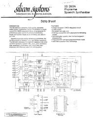
27C512 EPROM Data Sheet.pdf - Downloads.reactivemicro.com
27C512 EPROM Data Sheet.pdf - Downloads.reactivemicro.com
27C512 EPROM Data Sheet.pdf - Downloads.reactivemicro.com

Create successful ePaper yourself
Turn your PDF publications into a flip-book with our unique Google optimized e-Paper software.
M<strong>27C512</strong>DEVICE OPERATIONThe modes of operations of the M<strong>27C512</strong> are listedin the Operating Modes table. A single powersupply is required in the read mode. All inputs areTTL levels except for GV PP and 12V on A9 forElectronic Signature.Read ModeThe M<strong>27C512</strong> has two control functions, both ofwhich must be logically active in order to obtaindata at the outputs. Chip Enable (E) is the powercontrol and should be used for device selection.Output Enable (G) is the output control and shouldbe used to gate data to the output pins, independentof device selection. Assuming that the addressesare stable, the address access time(t AVQV ) is equal to the delay from E to output(t ELQV ). <strong>Data</strong> is available at the output after a delayof t GLQV from the falling edge of G, assuming thatE has been low and the addresses have been stablefor at least t AVQV -t GLQV .Standby ModeThe M<strong>27C512</strong> has a standby mode which reducesthe active current from 30mA to 100µA TheM<strong>27C512</strong> is placed in the standby mode by applyinga CMOS high signal to the E input. When in thestandby mode, the outputs are in a high impedancestate, independent of the GV PP input.Table 2. Operating ModesMode E GV PP A9 Q7-Q0Read V IL V IL X <strong>Data</strong> OutOutput Disable V IL V IH X Hi-ZProgram V IL Pulse V PP X <strong>Data</strong> InProgram Inhibit V IH V PP X Hi-ZStandby V IH X X Hi-ZElectronic Signature V IL V IL V ID CodesNote: X = V IH or V IL , V ID = 12V ± 0.5V.Table 3. Electronic SignatureIdentifier A0 Q7 Q6 Q5 Q4 Q3 Q2 Q1 Q0 Hex <strong>Data</strong>Manufacturer’s Code V IL 0 0 1 0 0 0 0 0 20hDevice Code V IH 0 0 1 1 1 1 0 1 3DhTwo Line Output ControlBecause <strong>EPROM</strong>s are usually used in largermemory arrays, the product features a 2 line controlfunction which ac<strong>com</strong>modates the use of multiplememory connection. The two line controlfunction allows:a. the lowest possible memory powerdissipation,b. <strong>com</strong>plete assurance that output buscontention will not occur.For the most efficient use of these two controllines, E should be decoded and used as the primarydevice selecting function, while G should bemade a <strong>com</strong>mon connection to all devices in thearray and connected to the READ line from thesystem control bus. This ensures that all deselectedmemory devices are in their low power standbymode and that the output pins are only activewhen data is required from a particular memorydevice.System ConsiderationsThe power switching characteristics of AdvancedCMOS <strong>EPROM</strong>s require careful decoupling of thedevices. The supply current, I CC , has three segmentsthat are of interest to the system designer:the standby current level, the active current level,and transient current peaks that are produced bythe falling and rising edges of E. The magnitude ofthe transient current peaks is dependent on thecapacitive and inductive loading of the device atthe output. The associated transient voltage peakscan be suppressed by <strong>com</strong>plying with the two lineoutput control and by properly selected decouplingcapacitors. It is re<strong>com</strong>mended that a 0.1µF ceramiccapacitor be used on every device between V CCand V SS . This should be a high frequency capacitorof low inherent inductance and should beplaced as close to the device as possible. In addi-6/22