TDA7384 - 320Volt
TDA7384 - 320Volt
TDA7384 - 320Volt
- No tags were found...

You also want an ePaper? Increase the reach of your titles
YUMPU automatically turns print PDFs into web optimized ePapers that Google loves.
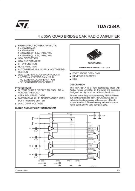
®<strong>TDA7384</strong>A4 x 35W QUAD BRIDGE CAR RADIO AMPLIFIERHIGH OUTPUT POWER CAPABILITY:4 x 40W/4Ω MAX.4 x 35W/4Ω EIAJ4 x 25W/4Ω @ 14.4V, 1KHz, 10%4 x 22W/4Ω @ 13.2V, 1KHz, 10%LOW DISTORTIONLOW OUTPUT NOISEST-BY FUNCTIONMUTE FUNCTIONAUTOMUTE AT MIN. SUPPLY VOLTAGE DE-TECTIONLOW EXTERNAL COMPONENT COUNT:– INTERNALLY FIXED GAIN (26dB)– NO EXTERNAL COMPENSATION– NO BOOTSTRAP CAPACITORSPROTECTIONS:OUTPUT SHORT CIRCUIT TO GND, TO VS,ACROSS THE LOADVERY INDUCTIVE LOADSOVERRATING CHIP TEMPERATURE WITHSOFT THERMAL LIMITERLOAD DUMP VOLTAGEBLOCK AND APPLICATION DIAGRAMFLEXIWATT25ORDERING NUMBER: <strong>TDA7384</strong>AFORTUITOUS OPEN GNDREVERSED BATTERYESDDESCRIPTIONThe <strong>TDA7384</strong>A is a new technology class ABAudio Power Amplifier in Flexiwatt 25 packagedesigned for high end car radio applications.Thanks to the fully complementary PNP/NPN outputconfiguration the <strong>TDA7384</strong>A allows a rail torail output voltage swing with no need of bootstrapcapacitors. The extremely reduced componentscount allows very compact sets.Vcc1Vcc2470µF100nFST-BYIN1IN2IN3IN4MUTE0.1µF0.1µF0.1µF0.1µFAC-GNDSVR TAB S-GND0.47µF 47µFN.C.OUT1+OUT1-PW-GNDOUT2+OUT2-PW-GNDOUT3+OUT3-PW-GNDOUT4+OUT4-PW-GNDD99AU1018October 19991/9
<strong>TDA7384</strong>AABSOLUTE MAXIMUM RATINGSSymbol Parameter Value UnitV CC Operating Supply Voltage 18 VV CC (DC) DC Supply Voltage 28 VVCC (pk) Peak Supply Voltage (t = 50ms) 50 VI OOutput Peak Current:Repetitive (Duty Cycle 10% at f = 10Hz)Non Repetitive (t = 100µs)P tot Power dissipation, (T case =70°C) 80 WT j Junction Temperature 150 °CT stg Storage Temperature – 55 to 150 °C4.55.5AAPIN CONNECTION (Top view)1 25TABP-GND2ST-BYOUT2+P-GND1OUT1+SVRIN1IN2S-GNDIN4IN3AC-GNDOUT3+P-GND3VCCOUT4+MUTEOUT2-VCCOUT1-OUT3-OUT4-P-GND4HSDD94AU159ATHERMAL DATASymbol Parameter Value UnitR th j-case Thermal Resistance Junction to Case Max. 1 °C/W2/9
<strong>TDA7384</strong>AELECTRICAL CHARACTERISTICS (VS = 14.4V; f = 1KHz; Rg = 600Ω;RL =4Ω;Tamb =25°C;Refer to the test and application diagram, unless otherwise specified.)Symbol Parameter Test Condition Min. Typ. Max. UnitI q1 Quiescent Current R L = ∞ 120 190 350 mAV OS Output Offset Voltage Play Mode ±80 mVdV OS During mute ON/OFF output±80 mVoffset voltageGv Voltage Gain 25 26 27 dBdG v Channel Gain Unbalance ±1 dBP o Output Power V S = 13.2V; THD = 10%V S = 13.2V; THD = 0.8%V S = 14,4V; THD = 10%Po EIAJ EIAJ Output Power (*) VS = 13.7V 32 35 WPo max. Output Power (*) VS = 14.4V 38 40 WTHD Distortion P o = 4W 0.04 0.15 %e No Output Noise ”A Weighted”Bw = 20Hz to 20KHzSVR Supply Voltage Rejection f = 100Hz; V r = 1Vrms 50 65 dBf ch High Cut-Off Frequency P O = 0.5W 100 200 KHzR i Input Impedance 70 100 KΩC T Cross Talk f = 1KHz P O =4Wf = 10KHz P O =4WI SB St-By Current Consumption V St-By = 1.5V 100 µAI pin4 St-by pin Current VSt-By = 1.5V to 3.5V ±10 µAV SB out St-By Out Threshold Voltage (Amp: ON) 3.5 VV SB in St-By in Threshold Voltage (Amp: OFF) 1.5 VA M Mute Attenuation P Oref =4W 80 90 dBVM out Mute Out Threshold Voltage (Amp: Play) 3.5 VVM in Mute In Threshold Voltage (Amp: Mute) 1.5 VV AM in V S Automute Threshold (Amp: Mute)Att ≥ 80dB; P Oref =4W(Amp: Play)6.5 VAtt < 0.1dB; PO = 0.5W 7.6 8.5 VI pin22 Muting Pin Current V MUTE = 1.5V(Sourced Current)5 11 20 µA(*) Saturated square wave output.20152460502217265070706070100––WWWµVµVdBdB3/9
<strong>TDA7384</strong>AFigure 1: Standard Test and Application CircuitC80.1µFC72200µFVcc1-2Vcc3-4ST-BYMUTEIN1R110KR247KC10.1µFC91µFC101µF422116 20987523OUT1OUT2IN21217C2 0.1µF18OUT3IN31519C3 0.1µF21IN41424OUT4C4 0.1µFS-GND1316 10 25 123C50.47µFSVRC647µFHSDTABD95AU335B4/9
<strong>TDA7384</strong>AFigure 3: Quiescent Current vs. Supply VoltageFigure 4: Quiescent Output Voltage vs. SupplyVoltageFigure 5: Output Power vs. Supply VoltageFigure 6: Distortion vs. Output PowerFigure 7: Distortion vs. FrequencyFigure 8: Supply Voltage Rejection vs.Frequency.V S =14.4VRL =4ΩP O =1W6/9
<strong>TDA7384</strong>ADIM.mminchMIN. TYP. MAX. MIN. TYP. MAX.A 4.45 4.50 4.65 0.175 0.177 0.183B 1.80 1.90 2.00 0.070 0.074 0.079C 1.40 0.055D 0.75 0.90 1.05 0.029 0.035 0.041E 0.37 0.39 0.42 0.014 0.015 0.016F (1) 0.57 0.022G 0.80 1.00 1.20 0.031 0.040 0.047G1 23.75 24.00 24.25 0.935 0.945 0.955H (2) 28.90 29.23 29.30 1.138 1.150 1.153H1 17.00 0.669H2 12.80 0.503H3 0.80 0.031L (2) 22.07 22.47 22.87 0.869 0.884 0.904L1 18.57 18.97 19.37 0.731 0.747 0.762L2 (2) 15.50 15.70 15.90 0.610 0.618 0.626L3 7.70 7.85 7.95 0.303 0.309 0.313L4 5 0.197L5 3.5 0.138M 3.70 4.00 4.30 0.145 0.157 0.169M1 3.60 4.00 4.40 0.142 0.157 0.173N 2.20 0.086O 2 0.079R 1.70 0.067R1 0.5 0.02R2 0.3 0.12R3 1.25 0.049R4 0.50 0.019V5°(Typ.)V13° (Typ.)V220° (Typ.)V345° (Typ.)(1): dam-bar protusion not included(2): molding protusion includedOUTLINE ANDMECHANICAL DATAFlexiwatt25V3H3HH1H2AOR3L2L3 L4NR4V2RR2LL1V1V1R2R1DL5 R1 R1VGG1FMEM1BCVFLEX25ME8/9