AN678 - 320Volt
AN678 - 320Volt
AN678 - 320Volt
- No tags were found...

Create successful ePaper yourself
Turn your PDF publications into a flip-book with our unique Google optimized e-Paper software.
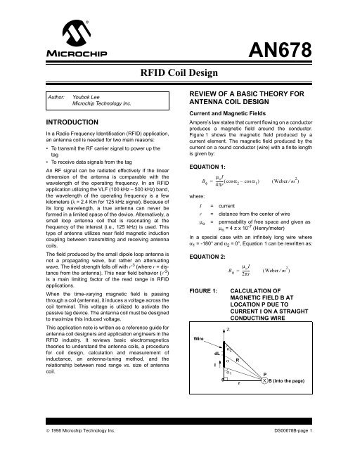
MRFID Coil Design<strong>AN678</strong>Author:Youbok LeeMicrochip Technology Inc.INTRODUCTIONIn a Radio Frequency Identification (RFID) application,an antenna coil is needed for two main reasons:• To transmit the RF carrier signal to power up thetag• To receive data signals from the tagAn RF signal can be radiated effectively if the lineardimension of the antenna is comparable with thewavelength of the operating frequency. In an RFIDapplication utilizing the VLF (100 kHz – 500 kHz) band,the wavelength of the operating frequency is a fewkilometers (λ = 2.4 Km for 125 kHz signal). Because ofits long wavelength, a true antenna can never beformed in a limited space of the device. Alternatively, asmall loop antenna coil that is resonating at thefrequency of the interest (i.e., 125 kHz) is used. Thistype of antenna utilizes near field magnetic inductioncoupling between transmitting and receiving antennacoils.The field produced by the small dipole loop antenna isnot a propagating wave, but rather an attenuatingwave. The field strength falls off with r -3 (where r = distancefrom the antenna). This near field behavior (r -3 )is a main limiting factor of the read range in RFIDapplications.When the time-varying magnetic field is passingthrough a coil (antenna), it induces a voltage across thecoil terminal. This voltage is utilized to activate thepassive tag device. The antenna coil must be designedto maximize this induced voltage.This application note is written as a reference guide forantenna coil designers and application engineers in theRFID industry. It reviews basic electromagneticstheories to understand the antenna coils, a procedurefor coil design, calculation and measurement ofinductance, an antenna-tuning method, and therelationship between read range vs. size of antennacoil.REVIEW OF A BASIC THEORY FORANTENNA COIL DESIGNCurrent and Magnetic FieldsAmpere’s law states that current flowing on a conductorproduces a magnetic field around the conductor.Figure 1 shows the magnetic field produced by acurrent element. The magnetic field produced by thecurrent on a round conductor (wire) with a finite lengthis given by:EQUATION 1:B φwhere:I = currentr = distance from the center of wireµ o = permeability of free space and given asµ o =4 π x 10 -7 (Henry/meter)In a special case with an infinitely long wire whereα 1 = -180° and α 2 = 0°, Equation 1 can be rewritten as:EQUATION 2:FIGURE 1:Wireµ oI= -------- ( cosα 4πr 2– cosα 1) ( Weber ⁄ m 2 )dLIΖB φµ oI= -------- ( Weber ⁄ m 2 )2πrCALCULATION OFMAGNETIC FIELD B ATLOCATION P DUE TOCURRENT I ON A STRAIGHTCONDUCTING WIREα 2αRα 1P0rX B (into the page)© 1998 Microchip Technology Inc. DS00678B-page 1
<strong>AN678</strong>The magnetic field produced by a circular loop antennacoil with N-turns as shown in Figure 2 is found by:EQUATION 3:where:µ oINa 2B z= --------------------------------2( a 2 + r 2 ) 3⁄2a = radius of loopEquation 3 indicates that the magnetic field producedby a loop antenna decays with 1/r 3 as shown inFigure 3. This near-field decaying behavior of themagnetic field is the main limiting factor in the readrange of the RFID device. The field strength ismaximum in the plane of the loop and directlyproportional to the current (I), the number of turns (N),and the surface area of the loop.Equation 3 is frequently used to calculate theampere-turn requirement for read range. A fewexamples that calculate the ampere-turns and the fieldintensity necessary to power the tag will be given in thefollowing sections.FIGURE 2:µ oINa 2I1= ----------------- ⎛----⎞2 ⎝r 3 for r 2 >>a 2 coilα⎠aFIGURE 3:Byr -3CALCULATION OFMAGNETIC FIELD B ATLOCATION P DUE TOCURRENT I ON THE LOOPRrB zPDECAYING OF THEMAGNETIC FIELD B VS.DISTANCE rzrNote:The magnetic field produced by aloop antenna drops off with r -3 .DS00678B-page 2© 1998 Microchip Technology Inc.
<strong>AN678</strong>INDUCED VOLTAGE IN ANTENNACOILFaraday’s law states a time-varying magnetic fieldthrough a surface bounded by a closed path induces avoltage around the loop. This fundamental principlehas important consequences for operation of passiveRFID devices.Figure 4 shows a simple geometry of an RFIDapplication. When the tag and reader antennas arewithin a proximity distance, the time-varying magneticfield B that is produced by a reader antenna coilinduces a voltage (called electromotive force or simplyEMF) in the tag antenna coil. The induced voltage inthe coil causes a flow of current in the coil. This is calledFaraday’s law.The induced voltage on the tag antenna coil is equal tothe time rate of change of the magnetic flux Ψ.EQUATION 4:where:V= – N dΨ -------dtN = number of turns in the antenna coilΨ = magnetic flux through each turnThe negative sign shows that the induced voltage actsin such a way as to oppose the magnetic flux producingit. This is known as Lenz’s Law and it emphasizes thefact that the direction of current flow in the circuit issuch that the induced magnetic field produced by theinduced current will oppose the original magnetic field.The magnetic flux Ψ in Equation 4 is the total magneticfield B that is passing through the entire surface of theantenna coil, and found by:EQUATION 5:where:ψ=∫B· dSB = magnetic field given in Equation 3S = surface area of the coil• = inner product (cosine angle betweentwo vectors) of vectors B and surfacearea SNote: Both magnetic field B and surface S arevector quantities.The inner product presentation of two vectors inEquation 5 suggests that the total magnetic flux ψ thatis passing through the antenna coil is affected by an orientationof the antenna coils. The inner product of twovectors becomes maximized when the two vectors arein the same direction. Therefore, the magnetic flux thatis passing through the tag coil will become maximizedwhen the two coils (reader coil and tag coil) are placedin parallel with respect to each other.FIGURE 4:A BASIC CONFIGURATION OF READER AND TAG ANTENNAS IN AN RFIDAPPLICATIONTag CoilV = V 0 sin(ωt)TagB = B 0 sin(ωt)Reader CoilReaderElectronicsTuning CircuitI = I 0 sin(ωt)© 1998 Microchip Technology Inc. DS00678B-page 3
<strong>AN678</strong>From Equations 3, 4, and 5, the induced voltage V 0 foran untuned loop antenna is given by:EQUATION 6:where:f = frequency of the arrival signalN = number of turns of coil in the loopS = area of the loop in square meters (m 2 )B o = strength of the arrival signalα = angle of arrival of the signalIf the coil is tuned (with capacitor C) to the frequency ofthe arrival signal (125 kHz), the output voltage V o willrise substantially. The output voltage found inEquation 6 is multiplied by the loaded Q (QualityFactor) of the tuned circuit, which can be varied from 5to 50 in typical low-frequency RFID applications:EQUATION 7:where the loaded Q is a measure of the selectivity ofthe frequency of the interest. The Q will be defined inEquations 30, 31, and 37 for general, parallel, andserial resonant circuit, respectively.FIGURE 5:V o= 2πfNSB ocosαV o= 2πf oNQSB ocosαORIENTATION DEPENDENCYOF THE TAG ANTENNA.B-fieldLine of axis(Tag)EXAMPLE 1:EXAMPLE 2:B-FIELD REQUIREMENTThe strength of the B-field that is needed to turn onthe tag can be calculated from Equation 7:EQUATION 8:B oVo= -----------------------------------2πf oNQScosα72.4 ( )= -------------------------------------------------------------------------------------------( 2π) ( 125 kHz) ( 100) ( 15) ( 38.71cm 2 )≈ 1.5 µWb/m 2where the following parameters are used in theabove calculation:tag coil size = 2 x 3 inches =38.71 cm 2 : (creditcard size)frequency = 125 kHznumber of turns = 100Q of antenna coil = 15AC coil voltageto turn on the tag = 7 Vcos α = 1 (normal direction,α = 0).NUMBER OF TURNS ANDCURRENT (AMPERE-TURNS) OF READER COILAssuming that the reader should provide a readrange of 10 inches (25.4 cm) with a tag given inExample 1, the requirement for the current andnumber of turns (Ampere-turns) of a reader coil thathas an 8 cm radius can be calculated fromEquation 3:EQUATION 9:( NI)2B z( a 2 + r 2 )= ------------------------------µa 23⁄2αTag=21.5 ( × 10 – 6 )( 0.08 2 + 0.254 2 )-------------------------------------------------------------------------( 4π × 10 – 7 )( 0.08)3 ⁄ 2=7.04 ( ampere - turns)The induced voltage developed across the loopantenna coil is a function of the angle of the arrival signal.The induced voltage is maximized when theantenna coil is placed perpendicular to the direction ofthe incoming signal where α = 0.This is an attainable number. If, however, we wish tohave a read range of 20 inches (50.8 cm), it can befound that NI increases to 48.5 ampere-turns. At25.2 inches (64 cm), it exceeds 100 ampere-turns.DS00678B-page 4© 1998 Microchip Technology Inc.
<strong>AN678</strong>For a longer read range, it is instructive to considerincreasing the radius of the coil. For example, bydoubling the radius (16 cm) of the loop, theampere-turns requirement for the same read range (10inches: 25.4 cm) becomes:EQUATION 10:21.5 ( × 10 – 6 )( 0.16 2 + 0.25 2 )NI = ----------------------------------------------------------------------( 4π × 10 – 7 )( 0.16 2 )= 2.44 (ampere-turns)3 ⁄ 2At a read range of 20 inches (50.8 cm), theampere-turns becomes 13.5 and at 25.2 inches (64cm), 26.8. Therefore, for a longer read range,increasing the tag size is often more effective thanincreasing the coil current. Figure 6 shows the relationshipbetween the read range and the ampere-turns(IN).The optimum radius of loop that requires the minimumnumber of ampere-turns for a particular read range canbe found from Equation 3 such as:EQUATION 11:where:(NI K a2 + r 2 )= -----------------------KBy taking derivative with respect to the radius a,µ oa 22B z= --------dNI------------- ( ) K 3⁄ 2 ( a2 + r 2 ) 1 ⁄ 2( 2a 3 )–2a( a 2 + r 2 ) 3⁄2= -----------------------------------------------------------------------------------------------daa 43--2FIGURE 6:AMPERE-TURNS VS. READRANGE FOR AN ACCESSCONTROL CARD (CREDITCARD SIZE)(K a2 – 2r 2 )( a 2 + r 2 ) 1 ⁄ 2= -----------------------------------------------------a 3The above equation becomes minimized when:NI for 1.5 µ-Weber/m 21001010.10.01a = 50 cma = 20 cma = 10 cma = 5 cma = 2 cma = sqrt(2)*r0.001 0.001 0.01 0.1 1 10r (m)Note:B O = 1.5 µWb/m 2 is used.The above result shows a relationship between theread range vs. tag size. The optimum radius is foundas:where:a 2 – 2r 2 = 0a = 2ra = radius of coilr = read rangeThe above result indicates that the optimum radius ofloop for a reader antenna is 1.414 times the readrange r.© 1998 Microchip Technology Inc. DS00678B-page 5
<strong>AN678</strong>WIRE TYPES AND OHMIC LOSSESWire Size and DC ResistanceThe diameter of electrical wire is expressed as theAmerican Wire Gauge (AWG) number. The gaugenumber is inversely proportional to diameter and thediameter is roughly doubled every six wire gauges. Thewire with a smaller diameter has higher DC resistance.The DC resistance for a conductor with a uniformcross-sectional area is found by:EQUATION 12:where:R DCl= ------ ( Ω)σSl = total length of the wireσ = conductivityS = cross-sectional areaTable 1 shows the diameter for bare andenamel-coated wires, and DC resistance.AC Resistance of WireAt DC, charge carriers are evenly distributed throughthe entire cross section of a wire. As the frequencyincreases, the reactance near the center of the wireincreases. This results in higher impedance to the currentdensity in the region. Therefore, the charge movesaway from the center of the wire and towards the edgeof the wire. As a result, the current density decreasesin the center of the wire and increases near the edge ofthe wire. This is called a skin effect. The depth into theconductor at which the current density falls to 1/e, or37% of its value along the surface, is known as the skindepth and is a function of the frequency and the permeabilityand conductivity of the medium. The skin depthis given by:EXAMPLE 3:The skin depth for a copper wire at 125 kHz can becalculated as:EQUATION 14:The wire resistance increases with frequency, and theresistance due to the skin depth is called an ACresistance. An approximated formula for the ac resistanceis given by:EQUATION 15:where:δ =a = coil radius1--------------------------------------------------------------------πf( 4π × 10 – 7 )( 5.8 × 10 – 7 )0.06608= ------------------ ( m)f= 0.187 ( mm)1R ac≈ ------------- = ( R2σπδ DC)-----a2δ( Ω)For copper wire, the loss is approximated by the DCresistance of the coil, if the wire radius is greater than0.066 ⁄ f cm. At 125 kHz, the critical radius is 0.019cm. This is equivalent to #26 gauge wire. Therefore, forminimal loss, wire gauge numbers of greater than #26should be avoided if coil Q is to be maximized.EQUATION 13:δ=1----------------πfµσwhere:f = frequencyµ = permeability of materialσ = conductivity of the materialDS00678B-page 6© 1998 Microchip Technology Inc.
<strong>AN678</strong>TABLE 1:AWG WIRE CHARTWireSize(AWG)Dia. inMils(bare)Dia. inMils(coated)Ohms/1000 ft.CrossSection(mils)1 289.3 — 0.126 836902 287.6 — 0.156 663603 229.4 — 0.197 526204 204.3 — 0.249 417405 181.9 — 0.313 330906 162.0 — 0.395 262407 166.3 — 0.498 208208 128.5 131.6 0.628 165109 114.4 116.3 0.793 1309010 101.9 106.2 0.999 1038011 90.7 93.5 1.26 823012 80.8 83.3 1.59 653013 72.0 74.1 2.00 518014 64.1 66.7 2.52 411015 57.1 59.5 3.18 326016 50.8 52.9 4.02 258017 45.3 47.2 5.05 206018 40.3 42.4 6.39 162019 35.9 37.9 8.05 129020 32.0 34.0 10.1 102021 28.5 30.2 12.8 81222 25.3 28.0 16.2 64023 22.6 24.2 20.3 51124 20.1 21.6 25.7 40425 17.9 19.3 32.4 320Note: 1 mil = 2.54 x 10 -3 cmWireSize(AWG)Dia. inMils(bare)Dia. inMils(coated)26 15.9 17.2 41.0 25327 14.2 15.4 51.4 20228 12.6 13.8 65.3 15929 11.3 12.3 81.2 12330 10.0 11.0 106.0 10031 8.9 9.9 131 79.232 8.0 8.8 162 64.033 7.1 7.9 206 50.434 6.3 7.0 261 39.735 5.6 6.3 331 31.436 5.0 5.7 415 25.037 4.5 5.1 512 20.238 4.0 4.5 648 16.039 3.5 4.0 847 12.240 3.1 3.5 1080 9.6141 2.8 3.1 1320 7.8442 2.5 2.8 1660 6.2543 2.2 2.5 2140 4.8444 2.0 2.3 2590 4.0045 1.76 1.9 3350 3.1046 1.57 1.7 4210 2.4647 1.40 1.6 5290 1.9648 1.24 1.4 6750 1.5449 1.11 1.3 8420 1.2350 0.99 1.1 10600 0.98Note: 1 mil = 2.54 x 10 -3 cmOhms/1000 ft.CrossSection(mils)© 1998 Microchip Technology Inc. DS00678B-page 7
<strong>AN678</strong>INDUCTANCE OF VARIOUSANTENNA COILSThe electrical current flowing through a conductorproduces a magnetic field. This time-varying magneticfield is capable of producing a flow of current throughanother conductor. This is called inductance. Theinductance L depends on the physical characteristics ofthe conductor. A coil has more inductance than astraight wire of the same material, and a coil with moreturns has more inductance than a coil with fewer turns.The inductance L of inductor is defined as the ratio ofthe total magnetic flux linkage to the current Ι throughthe inductor: i.e.,EQUATION 16:where:NψL = -------(Henry)IN = number of turnsI = currentΨ = magnetic fluxIn a typical RFID antenna coil for 125 kHz, theinductance is often chosen as a few (mH) for a tag andfrom a few hundred to a few thousand (µH) for a reader.For a coil antenna with multiple turns, greaterinductance results with closer turns. Therefore, the tagantenna coil that has to be formed in a limited spaceoften needs a multi-layer winding to reduce the numberof turns.The design of the inductor would seem to be a relativelysimple matter. However, it is almost impossible toconstruct an ideal inductor because:a) The coil has a finite conductivity that results inlosses, andb) The distributed capacitance exists betweenturns of a coil and between the conductor andsurrounding objects.The actual inductance is always a combination ofresistance, inductance, and capacitance. The apparentinductance is the effective inductance at any frequency,i.e., inductive minus the capacitive effect. Variousformulas are available in literatures for the calculationof inductance for wires and coils [1, 2] .The parameters in the inductor can be measured. Forexample, an HP 4285 Precision LCR Meter canmeasure the inductance, resistance, and Q of the coil.Inductance of a Straight WireThe inductance of a straight wound wire shown inFigure 1 is given by:EQUATION 17:where:EXAMPLE 4:CALCULATION OFINDUCTANCE FOR ASTRAIGHT WIREInductance of a Single Layer CoilThe inductance of a single layer coil shown in Figure 7can be calculated by:EQUATION 19:where:l and a = length and radius of wire in cm,respectively.a = coil radius (cm)l = coil length (cm)N = number of turnsFIGURE 7:L = 0.002l 2l 3log e---- – -- ( µH)a 4The inductance of a wire with 10 feet (304.8 cm)long and 2 mm diameter is calculated as follows:EQUATION 18:aL = 0.002( 304.8) ln 2304.8 ( )--------------------⎝⎛ 0.1 ⎠⎞ –==0.60967( 7.965)4.855 ( µH)3--4( aN) 2L = ------------------------------- ( µH)22.9l + 25.4aA SINGLE LAYER COILlNote:For best Q of the coil, the length shouldbe roughly the same as the diameter ofthe coil.DS00678B-page 8© 1998 Microchip Technology Inc.
<strong>AN678</strong>Inductance of a Circular Loop Antenna Coilwith MultilayerTo form a big inductance coil in a limited space, it ismore efficient to use multilayer coils. For this reason, atypical RFID antenna coil is formed in a planarmulti-turn structure. Figure 8 shows a cross section ofthe coil. The inductance of a circular ring antenna coilis calculated by an empirical formula [2] :EQUATION 20:where:a = average radius of the coil in cmN = number of turnsb = winding thickness in cmh = winding height in cmFIGURE 8:baXA CIRCULAR LOOP AIR COREANTENNA COIL WITHN-TURNSThe number of turns needed for a certain inductancevalue is simply obtained from Equation 20 such that:EQUATION 21:0.31( aN) 2L = ---------------------------------- ( µH)6a + 9h + 10bN-Turn CoilN=haL µH( 6a + 9h + 10b)-------------------------------------------------( 0.31)a 2center of coilbEXAMPLE 5:EXAMPLE ON NUMBER OFTURNSEquation 21 results in N = 200 turns for L = 3.87 mHwith the following coil geometry:a = 1 inch (2.54 cm)h = 0.05 cmb = 0.5 cmTo form a resonant circuit for 125 kHz, it needs acapacitor across the inductor. The resonant capacitorcan be calculated as:EQUATION 22:11C = ------------------( 2πf) 2 = ---------------------------------------------------------------------------L ( 4π 2 )( 125 × 10 3 )( 3.87 × 10 – 3 )= 419 ( pF)Inductance of a Square Loop Coil withMultilayerIf N is the number of turns and a is the side of thesquare measured to the center of the rectangular crosssection that has length b and depth c as shown inFigure 9, then [2] :EQUATION 23:L 0.008aN 2 a= ⎛2.303log ⎛-----------⎞10+ 0.2235 b ----------- + c + 0.726⎞( µH)⎝ ⎝b+ c⎠a ⎠The formulas for inductance are widely published andprovide a reasonable approximation for the relationshipbetween inductance and number of turns for a givenphysical size[1]-[4]. When building prototype coils, it iswise to exceed the number of calculated turns by about10%, and then remove turns to achieve resonance. Forproduction coils, it is best to specify an inductance andtolerance rather than a specific number of turns.FIGURE 9:N-Turn CoilA SQUARE LOOP ANTENNACOIL WITH MULTILAYERaabc(a) Top View(b) Cross Sectional View© 1998 Microchip Technology Inc. DS00678B-page 9
<strong>AN678</strong>CONFIGURATION OF ANTENNACOILSTag Antenna CoilAn antenna coil for an RFID tag can be configured inmany different ways, depending on the purpose of theapplication and the dimensional constraints. A typicalinductance L for the tag coil is a few (mH) for 125 kHzdevices. Figure 10 shows various configurations of tagantenna coils. The coil is typically made of a thin wire.The inductance and the number of turns of the coil canbe calculated by the formulas given in the previous section.An Inductance Meter is often used to measure theinductance of the coil. A typical number of turns of thecoil is in the range of 100 turns for 125 kHz and 3~5turns for 13.56 MHz devices.For a longer read range, the antenna coil must betuned properly to the frequency of interest (i.e.,125 kHz). Voltage drop across the coil is maximized byforming a parallel resonant circuit. The tuning is accomplishedwith a resonant capacitor that is connected inparallel to the coil as shown in Figure 10. The formulafor the resonant capacitor value is given inEquation 22.FIGURE 10:VARIOUS CONFIGURATIONS OF TAG ANTENNA COILN-turn Coil2aad = 2a2abC oC oC oDS00678B-page 10© 1998 Microchip Technology Inc.
<strong>AN678</strong>Reader Antenna CoilThe inductance for the reader antenna coil is typicallyin the range of a few hundred to a few thousandmicro-Henries (µH) for low frequency applications. Thereader antenna can be made of either a single coil thatis typically forming a series resonant circuit or a doubleloop (transformer) antenna coil that forms a parallelresonant circuit.The series resonant circuit results in minimumimpedance at the resonance frequency. Therefore, itdraws a maximum current at the resonance frequency.On the other hand, the parallel resonant circuit resultsin maximum impedance at the resonance frequency.Therefore, the current becomes minimized at the resonancefrequency. Since the voltage can be stepped upby forming a double loop (parallel) coil, the parallelresonant circuit is often used for a system where ahigher voltage signal is required.Figure 11 shows an example of the transformer loopantenna. The main loop (secondary) is formed withseveral turns of wire on a large frame, with a tuningcapacitor to resonate it to the resonance frequency(125 kHz). The other loop is called a coupling loop(primary), and it is formed with less than two or threeturns of coil. This loop is placed in a very closeproximity to the main loop, usually (but not necessarily)on the inside edge and not more than a couple of centimetersaway from the main loop. The purpose of thisloop is to couple signals induced from the main loop tothe reader (or vise versa) at a more reasonablematching impedance.The coupling (primary) loop provides an impedancematch to the input/output impedance of the reader. Thecoil is connected to the input/output signal driver in thereader electronics. The main loop (secondary) must betuned to resonate at the resonance frequency and isnot physically connected to the reader electronics.The coupling loop is usually untuned, but in somedesigns, a tuning capacitor C2 is placed in series withthe coupling loop. Because there are far fewer turns onthe coupling loop than the main loop, its inductance isconsiderably smaller. As a result, the capacitance toresonate is usually much larger.FIGURE 11:A TRANSFORMER LOOP ANTENNA FOR READERCoupling Coil(primary coil)C2To reader electronicsMain Loop(secondary coil)C1© 1998 Microchip Technology Inc. DS00678B-page 11
<strong>AN678</strong>RESONANCE CIRCUITS, QUALITYFACTOR Q, AND BANDWIDTHIn RFID applications, the antenna coil is an element ofresonant circuit and the read range of the device isgreatly affected by the performance of the resonantcircuit.Figures 12 and 13 show typical examples of resonantcircuits formed by an antenna coil and a tuningcapacitor. The resonance frequency (f o ) of the circuit isdetermined by:EQUATION 24:where:1f o= ------------------2π LCL = inductance of antenna coilC = tuning capacitanceThe resonant circuit can be formed either series orparallel.The series resonant circuit has a minimum impedanceat the resonance frequency. As a result, maximumcurrent is available in the circuit. This series resonantcircuit is typically used for the reader antenna.On the other hand, the parallel resonant circuit hasmaximum impedance at the resonance frequency. Itoffers minimum current and maximum voltage at theresonance frequency. This parallel resonant circuit isused for the tag antenna.Parallel Resonant CircuitFigure 12 shows a simple parallel resonant circuit. Thetotal impedance of the circuit is given by:EQUATION 25:where:Zjω ( )ω = angular frequency = 2πfR = load resistorThe ohmic resistance r of the coil is ignored. Themaximum impedance occurs when the denominator inthe above equation minimized such as:EQUATION 26:This is called a resonance condition and the resonancefrequency is given by:EQUATION 27:By applying Equation 26 into Equation 25, theimpedance at the resonance frequency becomes:EQUATION 28:jωL= --------------------------------------------( 1 – ω 2 LC) + j ωL ( Ω)------Rω 2 LC = 11f o= ------------------2π LCZ=RFIGURE 12:PARALLEL RESONANTCIRCUITRCLThe R and C in the parallel resonant circuit determinethe bandwidth, B, of the circuit.EQUATION 29:B1= -------------- ( Hz)2πRCDS00678B-page 12© 1998 Microchip Technology Inc.
<strong>AN678</strong>The quality factor, Q, is defined by various ways suchas:EQUATION 30:Q=Energy Stored in the System per One Cycle-----------------------------------------------------------------------------------------------------------------Energy Dissipated in the System per One CycleSeries Resonant CircuitA simple series resonant circuit is shown in Figure 13.The expression for the impedance of the circuit is:EQUATION 33:Zjω ( ) = r + j( X L– X C) ( Ω)=where:f o---Bf o = resonant frequencyB = bandwidthBy applying Equation 27 and Equation 29 intoEquation 30, the loaded Q in the parallel resonantcircuit is:EQUATION 31:The Q in parallel resonant circuit is directly proportionalto the load resistor R and also to the square root of theratio of capacitance and inductance in the circuit.When this parallel resonant circuit is used for the tagantenna circuit, the voltage drop across the circuit canbe obtained by combining Equations 7 and 31,EQUATION 32:Q = R C --- LV o= 2πf oNQSB ocosα= 2πf oN⎛R C ⎝--- ⎞L⎠SBo cosαwhere:r = ohmic resistance of the circuitEQUATION 34:EQUATION 35:The impedance in Equation 33 becomes minimizedwhen the reactance component cancelled out eachother such that X L = X C . This is called a resonancecondition. The resonance frequency is same as theparallel resonant frequency given in Equation 27.FIGURE 13:E INX L= 2πf oL ( Ω)1X c= -------------- ( Ω)2πf oCSERIES RESONANCECIRCUITr125 kHzCLE oThe above equation indicates that the induced voltagein the tag coil is inversely proportional to the squareroot of the coil inductance, but proportional to the numberof turns and surface area of the coil.The parallel resonant circuit can be used in the transformerloop antenna for a long-range reader as discussedin "Reader Antenna Coil" (Figure 11). Thevoltage in the secondary loop is proportional to the turnratio (n 2 /n 1 ) of the transformer loop. However, this highvoltage signal can corrupt the receiving signals. Forthis reason, a separate antenna is needed for receivingthe signal. This receiving antenna circuit should betuned to the modulating signal of the tag and detunnedto the carrier signal frequency for maximum readrange.The half power frequency bandwidth is determined byr and L, and given by:EQUATION 36:rB = --------- ( Hz)2πL© 1998 Microchip Technology Inc. DS00678B-page 13
<strong>AN678</strong>The quality factor, Q, in the series resonant circuit isgiven by:EQUATION 37:The series circuit forms a voltage divider; the voltagedrops in the coil is given by:EQUATION 38:orQ=f oB --- =EQUATION 39:V o--------V inωL------r1--rV o1= ----------- ; for unloaded circuitωCrL--- ; for loaded circuitCjX L=r ------------------------------- + jX L– jX V in cX LX LQ= ---------------------------------------------r 2 + ( X L– X c) 2= -----------------------------------------------⎛X r L– X c ⎞ 2= -------------------------------------------⎛X L– X c ⎞ 21 + ⎜---------------------⎟ 1 + ⎜---------------------⎟⎝ r ⎠ ⎝ r ⎠EXAMPLE 6:EXAMPLE 7:CIRCUIT PARAMETERS.If the series resistance of the circuit is 15 Ω, then theL and C values form a 125 kHz resonant circuit withQ = 8 are:EQUATION 40:X L= Qr s= 120ΩX L 120L = -------- = -------------------------------- = 153 ( µH)2πf 2π( 125 kHz)11C = ---------------- =2πfX L2π ---------------------------------------------- =( 125 kHz) ( 120)10.6 ( nF)CALCULATION OF READRANGELet us consider designing a reader antenna coil withL = 153 µH, diameter = 10 cm, and windingthickness and height are small compared to thediameter.The number of turns for the inductance can becalculated from Equation 21, resulting in 24 turns.If the current flow through the coil is 0.5 amperes,the ampere-turns becomes 12. Therefore, the readrange for this coil will be about 20 cm with a creditcard size tag.DS00678B-page 14© 1998 Microchip Technology Inc.
<strong>AN678</strong>Q and BandwidthFigure 14 shows the approximate frequency bands forcommon forms of Amplitude Shift Keying (ASK),Frequency Shift Keying (FSK), and Phase Shift Keying(PSK) modulation. For a full recovery of data signalfrom the tag, the reader circuit needs a bandwidth thatis at least twice the data rate. Therefore, if the data rateis 8 kHz for an ASK signal, the bandwidth must be atleast 16 kHz for a full recovery of the information that iscoming from the tag.The data rate for FSK (÷ 10) signal is 12.5 kHz.Therefore, a bandwidth of 25 kHz is needed for a fulldata recovery.The Q for this FSK (÷ 10) signal can be obtained fromEquation 30.EQUATION 41:Qf o= --- =B=5125 kHz--------------------25 kHzFor a PSK (÷ 2) signal, the data rate is 62.5 kHz (if thecarrier frequency is 125 kHz) therefore, the readercircuit needs 125 kHz of bandwidth. The Q in this caseis 1, and consequently the circuit becomesQ-independent.This problem may be solved by separating thetransmitting and receiving coils. The transmitting coilcan be designed with higher Q and the receiving coilwith lower Q.Limitation on QWhen designing a reader antenna circuit, thetemptation is to design a coil with very high Q. Thereare three important limitations to this approach.a) Very high voltages can cause insulationbreakdown in either the coil or resonantcapacitor.For example, a 1 ampere of current flow in a 2 mHcoil will produce a voltage drop of 1500 VPP. Suchvoltages are easy to obtain but difficult to isolate.In addition, in the case of single coil readerdesigns, recovery of the return signal from the tagmust be accomplished in the presence of thesehigh voltages.b) Tuning becomes critical.To implement a high Q antenna circuit, high voltagecomponents with a close tolerance and highstability would have to be used. Such parts aregenerally expensive and difficult to obtain.c) As the Q of the circuit gets higher, the amplitudeof the return signal relative to the power of thecarrier gets proportionally smaller complicatingits recovery by the reader circuit.FIGURE 14:Q FACTOR VS. MODULATION SIGNALS3530Q = 30252015Q = 14105PSK÷2Q = 8Q =5FSK ASK÷8,10FSKPSK÷8,10÷2050 75 100 125 150 175 200© 1998 Microchip Technology Inc. DS00678B-page 15
<strong>AN678</strong>Tuning MethodThe circuit must be tuned to the resonance frequencyfor a maximum performance (read range) of the device.Two examples of tuning the circuit are as follows:• Voltage Measurement Method:a) Set up a voltage signal source at theresonance frequency (125 kHz)b) Connect a voltage signal source across theresonant circuit.c) Connect an Oscilloscope across theresonant circuit.d) Tune the capacitor or the coil whileobserving the signal amplitude on theOscilloscope.e) Stop the tuning at the maximum voltage.• S-parameter or Impedance MeasurementMethod using Network Analyzer:a) Set up an S-Parameter Test Set (NetworkAnalyzer) for S11 measurement, and do acalibration.b) Measure the S11 for the resonant circuit.c) Reflection impedance or reflectionadmittance can be measured instead of theS11.d) Tune the capacitor or the coil until amaximum null (S11) occurs at theresonance frequency, f o . For the impedancemeasurement, the maximum peak will occurfor the parallel resonant circuit, andminimum peak for the series resonantcircuit.FIGURE 15:VOLTAGE VS. FREQUENCY FOR RESONANT CIRCUITVf ofFIGURE 16:FREQUENCY RESPONSES FOR RESONANT CIRCUITS11ZZf off off of(a) (b) (c)Note 1: (a) S11 Response, (b) Impedance Response for a Parallel Resonant Circuit, and (c)Impedance Response for a Series Resonant Circuit.2: In (a), the null at the resonance frequency represents a minimum input reflection atthe resonance frequency. This means the circuit absorbs the signal at the frequencywhile other frequencies are reflected back. In (b), the impedance curve has a peakat the resonance frequency. This is because the parallel resonant circuit has a maximumimpedance at the resonance frequency. (c) shows a response for the seriesresonant circuit. Since the series resonant circuit has a minimum impedance at theresonance frequency, a minimum peak occurs at the resonance frequency.DS00678B-page 16© 1998 Microchip Technology Inc.
<strong>AN678</strong>READ RANGE OF RFID DEVICESRead range is defined as a maximum communicationdistance between the reader and tag. The read rangeof typical passive RFID products varies from about1 inch to 1 meter, depending on system configuration.The read range of an RFID device is, in general,affected by the following parameters:a) Operating frequency and performance ofantenna coilsb) Q of antenna and tuning circuitc) Antenna orientationd) Excitation current and voltagee) Sensitivity of receiverf) Coding (or modulation) and decoding (ordemodulation) algorithmg) Number of data bits and detection(interpretation) algorithmh) Condition of operating environment (metallic,electrical noise), etc.With a given operating frequency, the above conditions(a – c) are related to the antenna configuration andtuning circuit. The conditions (d – e) are determined bya circuit topology of the reader. The condition (f) iscalled the communication protocol of the device, and(g) is related to a firmware program for data interpretation.Assuming the device is operating under a givencondition, the read range of the device is largelyaffected by the performance of the antenna coil. It isalways true that a longer read range is expected withthe larger size of the antenna. Figures 17 and 18 showtypical examples of the read range of various passiveRFID devices.FIGURE 17:READ RANGE VS. TAG SIZE FOR PROXIMITY APPLICATIONSTag0.5" diameterProximity ReaderAntenna(4" x 3")1 inch2 inches3 ~ 4 inchesTag1" diameterTag2" diameter4 ~ 5 inches3.37" x 2.125"(Credit Card Type: ISO Card)TagFIGURE 18:READ RANGE VS. TAG SIZE FOR LONG RANGE APPLICATIONSLong RangeReader Antenna(16" x 32")4 ~ 5 inches8 ~ 12 inches0.5" diameterTag1" diameterTag2" diameter18 ~ 22 inches Tag27 ~ 32 inches3.37" x 2.125"(Credit Card Type: ISO Card)Tag© 1998 Microchip Technology Inc. DS00678B-page 17
<strong>AN678</strong>REFERENCES1. Frederick W. Grover, Inductance Calculations:Working Formulas and Tables, DoverPublications, Inc., New York, NY., 1946.2. Keith Henry, Editor, Radio EngineeringHandbook, McGraw-Hill Book Company, NewYork, NY., 1963.3. V. G. Welsby, The Theory and Design ofInductance Coils, John Wiley and Sons, Inc.,1960.4. James K. Hardy, High Frequency Circuit Design,Reston Publishing Company, Inc., Reston,Virginia, 1975.DS00678B-page 18© 1998 Microchip Technology Inc.
<strong>AN678</strong>NOTES:© 1998 Microchip Technology Inc. DS00678B-page 19
MWORLDWIDE SALES AND SERVICEAMERICASCorporate OfficeMicrochip Technology Inc.2355 West Chandler Blvd.Chandler, AZ 85224-6199Tel: 602-786-7200 Fax: 602-786-7277Technical Support: 602 786-7627Web: http://www.microchip.comAtlantaMicrochip Technology Inc.500 Sugar Mill Road, Suite 200BAtlanta, GA 30350Tel: 770-640-0034 Fax: 770-640-0307BostonMicrochip Technology Inc.5 Mount Royal AvenueMarlborough, MA 01752Tel: 508-480-9990 Fax: 508-480-8575ChicagoMicrochip Technology Inc.333 Pierce Road, Suite 180Itasca, IL 60143Tel: 630-285-0071 Fax: 630-285-0075DallasMicrochip Technology Inc.14651 Dallas Parkway, Suite 816Dallas, TX 75240-8809Tel: 972-991-7177 Fax: 972-991-8588DaytonMicrochip Technology Inc.Two Prestige Place, Suite 150Miamisburg, OH 45342Tel: 937-291-1654 Fax: 937-291-9175DetroitMicrochip Technology Inc.42705 Grand River, Suite 201Novi, MI 48375-1727Tel: 248-374-1888 Fax: 248-374-2874Los AngelesMicrochip Technology Inc.18201 Von Karman, Suite 1090Irvine, CA 92612Tel: 714-263-1888 Fax: 714-263-1338New YorkMicrochip Technology Inc.150 Motor Parkway, Suite 202Hauppauge, NY 11788Tel: 516-273-5305 Fax: 516-273-5335San JoseMicrochip Technology Inc.2107 North First Street, Suite 590San Jose, CA 95131Tel: 408-436-7950 Fax: 408-436-7955AMERICAS (continued)TorontoMicrochip Technology Inc.5925 Airport Road, Suite 200Mississauga, Ontario L4V 1W1, CanadaTel: 905-405-6279 Fax: 905-405-6253ASIA/PACIFICHong KongMicrochip Asia PacificRM 3801B, Tower TwoMetroplaza223 Hing Fong RoadKwai Fong, N.T., Hong KongTel: 852-2-401-1200 Fax: 852-2-401-3431IndiaMicrochip Technology Inc.India Liaison OfficeNo. 6, Legacy, Convent RoadBangalore 560 025, IndiaTel: 91-80-229-0061 Fax: 91-80-229-0062JapanMicrochip Technology Intl. Inc.Benex S-1 6F3-18-20, ShinyokohamaKohoku-Ku, Yokohama-shiKanagawa 222-0033 JapanTel: 81-45-471- 6166 Fax: 81-45-471-6122KoreaMicrochip Technology Korea168-1, Youngbo Bldg. 3 FloorSamsung-Dong, Kangnam-KuSeoul, KoreaTel: 82-2-554-7200 Fax: 82-2-558-5934ShanghaiMicrochip TechnologyRM 406 Shanghai Golden Bridge Bldg.2077 Yan’an Road West, Hong Qiao DistrictShanghai, PRC 200335Tel: 86-21-6275-5700 Fax: 86 21-6275-5060ASIA/PACIFIC (continued)SingaporeMicrochip Technology Singapore Pte Ltd.200 Middle Road#07-02 Prime CentreSingapore 188980Tel: 65-334-8870 Fax: 65-334-8850Taiwan, R.O.CMicrochip Technology Taiwan10F-1C 207Tung Hua North RoadTaipei, Taiwan, ROCTel: 886-2-2717-7175 Fax: 886-2-2545-0139EUROPEUnited KingdomArizona Microchip Technology Ltd.505 Eskdale RoadWinnersh TriangleWokinghamBerkshire, England RG41 5TUTel: 44-1189-21-5858 Fax: 44-1189-21-5835FranceArizona Microchip Technology SARLZone Industrielle de la Bonde2 Rue du Buisson aux Fraises91300 Massy, FranceTel: 33-1-69-53-63-20 Fax: 33-1-69-30-90-79GermanyArizona Microchip Technology GmbHGustav-Heinemann-Ring 125D-81739 München, GermanyTel: 49-89-627-144 0 Fax: 49-89-627-144-44ItalyArizona Microchip Technology SRLCentro Direzionale ColleoniPalazzo Taurus 1 V. Le Colleoni 120041 Agrate BrianzaMilan, ItalyTel: 39-39-6899939 Fax: 39-39-68998839/8/98Microchip received ISO 9001 QualitySystem certification for its worldwideheadquarters, design, and waferfabrication facilities in January, 1997.Our field-programmable PICmicro 8-bit MCUs, Serial EEPROMs, relatedspecialty memory products and developmentsystems conform to the stringentquality standards of theInternational Standard Organization(ISO).All rights reserved. © 1998 Microchip Technology Incorporated. Printed in the USA. 9/98Printed on recycled paper.Information contained in this publication regarding device applications and the like is intended for suggestion only and may be superseded by updates. No representation or warrantyis given and no liability is assumed by Microchip Technology Incorporated with respect to the accuracy or use of such information, or infringement of patents or other intellectualproperty rights arising from such use or otherwise. Use of Microchip’s products as critical components in life support systems is not authorized except with express written approvalby Microchip. No licenses are conveyed, implicitly or otherwise, under any intellectual property rights. The Microchip logo and name are registered trademarks of Microchip TechnologyInc. in the U.S.A. and other countries. All rights reserved. All other trademarks mentioned herein are the property of their respective companies.DS00678B-page 20© 1998 Microchip Technology Inc.
AN680Passive RFID BasicsAuthor:INTRODUCTIONRadio Frequency Identification (RFID) systems useradio frequency to identify, locate and track people,assets, and animals. Passive RFID systems arecomposed of three components – an interrogator(reader), a passive tag, and a host computer. The tagis composed of an antenna coil and a silicon chip thatincludes basic modulation circuitry and non-volatilememory. The tag is energized by a time-varyingelectromagnetic radio frequency (RF) wave that istransmitted by the reader. This RF signal is called acarrier signal. When the RF field passes through anantenna coil, there is an AC voltage generated acrossthe coil. This voltage is rectified to supply power to thetag. The information stored in the tag is transmittedback to the reader. This is often called backscattering.By detecting the backscattering signal, the informationstored in the tag can be fully identified.DEFINITIONSPete SorrellsMicrochip Technology Inc.ReaderUsually a microcontroller-based unit with a wound outputcoil, peak detector hardware, comparators, andfirmware designed to transmit energy to a tag and readinformation back from it by detecting the backscattermodulation.TagAn RFID device incorporating a silicon memory chip(usually with on-board rectification bridge and other RFfront-end devices), a wound or printed input/output coil,and (at lower frequencies) a tuning capacitor.CarrierA Radio Frequency (RF) sine wave generated by thereader to transmit energy to the tag and retrieve datafrom the tag. In these examples the ISO frequencies of125 kHz and 13.56 MHz are assumed; higher frequenciesare used for RFID tagging, but the communicationmethods are somewhat different. 2.45 GHz, forexample, uses a true RF link. 125 kHz and 13.56 MHz,utilize transformer-type electromagnetic coupling.ModulationPeriodic fluctuations in the amplitude of the carrierused to transmit data back from the tag to the reader.Systems incorporating passive RFID tags operate inways that may seem unusual to anyone who alreadyunderstands RF or microwave systems. There is onlyone transmitter – the passive tag is not a transmitter ortransponder in the purest definition of the term, yet bidirectionalcommunication is taking place. The RF fieldgenerated by a tag reader (the energy transmitter) hasthree purposes:1. Induce enough power into the tag coil toenergize the tag. Passive tags have no batteryor other power source; they must derive allpower for operation from the reader field.125 kHz and 13.56 MHz tag designs mustoperate over a vast dynamic range of carrierinput, from the very near field (in the range of200 VPP) to the maximum read distance (in therange of 5 VPP).2. Provide a synchronized clock source to thetag. Many RFID tags divide the carrier frequencydown to generate an on-board clock forstate machines, counters, etc., and to derive thedata transmission bit rate for data returned tothe reader. Some tags, however, employ onboardoscillators for clock generation.3. Act as a carrier for return data from the tag.Backscatter modulation requires the reader topeak-detect the tag's modulation of the reader'sown carrier. See page 2 for additionalinformation on backscatter modulation.© 1998 Microchip Technology Inc. DS00680B-page 1
AN680SYSTEM HANDSHAKETypical handshake of a tag and reader is as follows:1. The reader continuously generates an RFcarrier sine wave, watching always for modulationto occur. Detected modulation of the fieldwould indicate the presence of a tag.2. A tag enters the RF field generated by thereader. Once the tag has received sufficientenergy to operate correctly, it divides down thecarrier and begins clocking its data to an outputtransistor, which is normally connected acrossthe coil inputs.3. The tag’s output transistor shunts the coil,sequentially corresponding to the data which isbeing clocked out of the memory array.4. Shunting the coil causes a momentaryfluctuation (dampening) of the carrier wave,which is seen as a slight change in amplitude ofthe carrier.5. The reader peak-detects the amplitude-modulateddata and processes the resulting bitstreamaccording to the encoding and data modulationmethods used.BACKSCATTER MODULATIONThis terminology refers to the communication methodused by a passive RFID tag to send data back to thereader. By repeatedly shunting the tag coil through atransistor, the tag can cause slight fluctuations in thereader’s RF carrier amplitude. The RF link behavesessentially as a transformer; as the secondary winding(tag coil) is momentarily shunted, the primary winding(reader coil) experiences a momentary voltage drop.The reader must peak-detect this data at about 60 dBdown (about 100 mV riding on a 100V sine wave) asshown in Figure 1.This amplitude-modulation loading of the reader’stransmitted field provides a communication path backto the reader. The data bits can then be encoded orfurther modulated in a number of ways.FIGURE 1:AMPLITUDE – MODULATEDBACKSCATTERING SIGNAL100 mV100VDS00680B-page 2© 1998 Microchip Technology Inc.
AN680DATA ENCODINGData encoding refers to processing or altering the databitstream in-between the time it is retrieved from theRFID chip’s data array and its transmission back to thereader. The various encoding algorithms affect errorrecovery, cost of implementation, bandwidth, synchronizationcapability, and other aspects of the systemdesign. Entire textbooks are written on the subject, butthere are several popular methods used in RFIDtagging today:1. NRZ (Non-Return to Zero) Direct. In thismethod no data encoding is done at all; the 1’sand 0’s are clocked from the data array directlyto the output transistor. A low in thepeak-detected modulation is a ‘0’ and a high is a‘1’.2. Differential Biphase. Several different forms ofdifferential biphase are used, but in general thebitstream being clocked out of the data array ismodified so that a transition always occurs onevery clock edge, and 1’s and 0’s are distinguishedby the transitions within the middle ofthe clock period. This method is used to embedclocking information to help synchronize thereader to the bitstream; and because it alwayshas a transition at a clock edge, it inherentlyprovides some error correction capability. Anyclock edge that does not contain a transition inthe data stream is in error and can be used toreconstruct the data.3. Biphase_L (Manchester). This is a variation ofbiphase encoding in which there is not always atransition at the clock edge.FIGURE 2:VARIOUS DATA CODING WAVEFORMSSIGNAL WAVEFORM DESCRIPTIONData1 0 1 1 0 0 0 1 1 0 1 0Digital DataBit RateCLKClock SignalNRZ_L(Direct)Non-Return to Zero – Level‘1’ is represented by logic high level.‘0’ is represented by logic low level.Biphase_L(Manchester)Biphase – Level (Split Phase)A level change occurs at middle ofevery bit clock period.‘1’ is represented by a high to lowlevel change at midclock.‘0’ is represented by a low to highlevel change at midclock.DifferentialBiphase_SDifferential Biphase – SpaceA level change occurs at middle ofevery bit clock period.‘1’ is represented by a change inlevel at start of clock.‘0’ is represented by no change inlevel at start of clock.© 1998 Microchip Technology Inc. DS00680B-page 3
AN680DATA MODULATIONAlthough all the data is transferred to the host byamplitude-modulating the carrier (backscatter modulation),the actual modulation of 1’s and 0’s is accomplishedwith three additional modulation methods:1. Direct. In direct modulation, the AmplitudeModulation of the backscatter approach is theonly modulation used. A high in the envelope isa ‘1’ and a low is a ‘0’. Direct modulation can providea high data rate but low noise immunity.2. FSK (Frequency Shift Keying). This form ofmodulation uses two different frequencies fordata transfer; the most common FSK mode isFc/8/10. In other words, a ‘0’ is transmitted as anamplitude-modulated clock cycle with periodcorresponding to the carrier frequency dividedby 8, and a ‘1’ is transmitted as anamplitude-modulated clock cycle period correspondingto the carrier frequency divided by 10.The amplitude modulation of the carrier thusswitches from Fc/8 to Fc/10 corresponding to 0'sand 1's in the bitstream, and the reader has onlyto count cycles between the peak-detectedclock edges to decode the data. FSK allows fora simple reader design, provides very strongnoise immunity, but suffers from a lower datarate than some other forms of data modulation.In Figure 3, FSK data modulation is used withNRZ encoding.3. PSK (Phase Shift Keying). This method of datamodulation is similar to FSK, except only onefrequency is used, and the shift between 1’s and0’s is accomplished by shifting the phase of thebackscatter clock by 180 degrees. Two commontypes of PSK are:• Change phase at any ‘0’, or• Change phase at any data change(0 to 1 or 1 to 0).PSK provides fairly good noise immunity, amoderately simple reader design, and a fasterdata rate than FSK. Typical applications utilize abackscatter clock of Fc/2, as shown in Figure 4.FIGURE 3: FSK MODULATED SIGNAL, FC/8 = 0, FC/10 = 18 cycles = 0 8 cycles = 0 10 cycles = 1 10 cycles = 1 8 cycles = 0FIGURE 4:PSK MODULATED SIGNALPhaseShiftPhaseShiftPhaseShiftPhaseShiftDS00680B-page 4© 1998 Microchip Technology Inc.
AN680ANTICOLLISIONIn many existing applications, a single-read RFID tag issufficient and even necessary: animal tagging andaccess control are examples. However, in a growingnumber of new applications, the simultaneous readingof several tags in the same RF field is absolutely critical:library books, airline baggage, garment, and retailapplications are a few.In order to read multiple tags simultaneously, the tagand reader must be designed to detect the conditionthat more than one tag is active. Otherwise, the tagswill all backscatter the carrier at the same time, and theamplitude-modulated waveforms shown in Figures 3and 4 would be garbled. This is referred to as acollision. No data would be transferred to the reader.The tag/reader interface is similar to a serial bus, eventhough the “bus” travels through the air. In a wired serialbus application, arbitration is necessary to prevent buscontention. The RFID interface also requires arbitrationso that only one tag transmits data over the “bus” at onetime.A number of different methods are in use and indevelopment today for preventing collisions; most arepatented or patent pending, but all are related tomaking sure that only one tag “talks” (backscatters) atany one time. See the MCRF355/360 Data Sheet(page 7) and the 13.56 MHz Reader Reference Design(page 47) chapters for more information regarding theMCRF355/360 anticollision protocol.© 1998 Microchip Technology Inc. DS00680B-page 5
WORLDWIDE SALES AND SERVICEAMERICASCorporate OfficeMicrochip Technology Inc.2355 West Chandler Blvd.Chandler, AZ 85224-6199Tel: 480-786-7200 Fax: 480-786-7277Technical Support: 480-786-7627Web: http://www.microchip.comAtlantaMicrochip Technology Inc.500 Sugar Mill Road, Suite 200BAtlanta, GA 30350Tel: 770-640-0034 Fax: 770-640-0307BostonMicrochip Technology Inc.5 Mount Royal AvenueMarlborough, MA 01752Tel: 508-480-9990 Fax: 508-480-8575ChicagoMicrochip Technology Inc.333 Pierce Road, Suite 180Itasca, IL 60143Tel: 630-285-0071 Fax: 630-285-0075DallasMicrochip Technology Inc.14651 Dallas Parkway, Suite 816Dallas, TX 75240-8809Tel: 972-991-7177 Fax: 972-991-8588DaytonMicrochip Technology Inc.Two Prestige Place, Suite 150Miamisburg, OH 45342Tel: 937-291-1654 Fax: 937-291-9175DetroitMicrochip Technology Inc.42705 Grand River, Suite 201Novi, MI 48375-1727Tel: 248-374-1888 Fax: 248-374-2874Los AngelesMicrochip Technology Inc.18201 Von Karman, Suite 1090Irvine, CA 92612Tel: 949-263-1888 Fax: 949-263-1338New YorkMicrochip Technology Inc.150 Motor Parkway, Suite 202Hauppauge, NY 11788Tel: 516-273-5305 Fax: 516-273-5335San JoseMicrochip Technology Inc.2107 North First Street, Suite 590San Jose, CA 95131Tel: 408-436-7950 Fax: 408-436-7955AMERICAS (continued)TorontoMicrochip Technology Inc.5925 Airport Road, Suite 200Mississauga, Ontario L4V 1W1, CanadaTel: 905-405-6279 Fax: 905-405-6253ASIA/PACIFICHong KongMicrochip Asia PacificUnit 2101, Tower 2MetroplazaKwai Fong, N.T., Hong KongTel: 852-2-401-1200 Fax: 852-2-401-3431IndiaMicrochip Technology Inc.India Liaison OfficeNo. 6, Legacy, Convent RoadBangalore 560 025, IndiaTel: 91-80-229-0061 Fax: 91-80-229-0062JapanMicrochip Technology Intl. Inc.Benex S-1 6F3-18-20, ShinyokohamaKohoku-Ku, Yokohama-shiKanagawa 222-0033 JapanTel: 81-45-471- 6166 Fax: 81-45-471-6122KoreaMicrochip Technology Korea168-1, Youngbo Bldg. 3 FloorSamsung-Dong, Kangnam-KuSeoul, KoreaTel: 82-2-554-7200 Fax: 82-2-558-5934ShanghaiMicrochip TechnologyRM 406 Shanghai Golden Bridge Bldg.2077 Yan’an Road West, Hong Qiao DistrictShanghai, PRC 200335Tel: 86-21-6275-5700 Fax: 86 21-6275-5060ASIA/PACIFIC (continued)SingaporeMicrochip Technology Singapore Pte Ltd.200 Middle Road#07-02 Prime CentreSingapore 188980Tel: 65-334-8870 Fax: 65-334-8850Taiwan, R.O.CMicrochip Technology Taiwan10F-1C 207Tung Hua North RoadTaipei, Taiwan, ROCTel: 886-2-2717-7175 Fax: 886-2-2545-0139EUROPEUnited KingdomArizona Microchip Technology Ltd.505 Eskdale RoadWinnersh TriangleWokinghamBerkshire, England RG41 5TUTel: 44 118 921 5858 Fax: 44-118 921-5835FranceArizona Microchip Technology SARLZone Industrielle de la Bonde2 Rue du Buisson aux Fraises91300 Massy, FranceTel: 33-1-69-53-63-20 Fax: 33-1-69-30-90-79GermanyArizona Microchip Technology GmbHGustav-Heinemann-Ring 125D-81739 München, GermanyTel: 49-89-627-144 0 Fax: 49-89-627-144-44ItalyArizona Microchip Technology SRLCentro Direzionale ColleoniPalazzo Taurus 1 V. Le Colleoni 120041 Agrate BrianzaMilan, ItalyTel: 39-39-6899939 Fax: 39-39-689988303/15/99Microchip received ISO 9001 QualitySystem certification for its worldwideheadquarters, design, and waferfabrication facilities in January, 1997.Our field-programmable PICmicro ® 8-bit MCUs, KEELOQ ® code hoppingdevices, Serial EEPROMs, relatedspecialty memory products and developmentsystems conform to the stringentquality standards of theInternational Standard Organization(ISO).All rights reserved. © 1999 Microchip Technology Incorporated. Printed in the USA. 4/99Printed on recycled paper.Information contained in this publication regarding device applications and the like is intended for suggestion only and may be superseded by updates. No representation or warrantyis given and no liability is assumed by Microchip Technology Incorporated with respect to the accuracy or use of such information, or infringement of patents or other intellectualproperty rights arising from such use or otherwise. Use of Microchip’s products as critical components in life support systems is not authorized except with express written approvalby Microchip. No licenses are conveyed, implicitly or otherwise, under any intellectual property rights. The Microchip logo and name are registered trademarks of Microchip TechnologyInc. in the U.S.A. and other countries. All rights reserved. All other trademarks mentioned herein are the property of their respective companies.DS00680B-page 6© 1999 Microchip Technology Inc.
AN707MCRF 355/360 ApplicationsAuthor:INTRODUCTIONDr. Youbok Lee, Ph.D.Microchip Technology Inc.The MCRF355 passive RFID device is designed for lowcost, multiple reading, and various high volume taggingapplications using a frequency band of 13.56 MHz. Thedevice has a total of 154 memory bits that can be reprogrammedby a contact programmer. The device operateswith a 70 kHz data rate, and asynchronously withrespect to the reader’s carrier. The device turns onwhen the coil voltage reaches 4 VPP and outputs datawith a Manchester format (see Figure 2-3 in the datasheet). With the given data rate (70 kHz), it takes about2.2 ms to transmit all 154 bits of the data. After transmittingall data, the device goes into a sleep mode for100 ms +/- 50%.The MCRF355 needs only an external parallel LC resonantcircuit that consists of an antenna coil and acapacitor for operation. The external LC componentsmust be connected between antenna A, B, and groundpads. The circuit formed between Antenna Pad A andthe ground pad must be tuned to the operating frequencyof the reader antenna.MODE OF OPERATIONThe device transmits data by tuning and detuning theresonant frequency of the external circuit. This processis accomplished by using an internal modulation gate(CMOS), that has a very low turn-on resistance (2 ~ 4ohms) between Drain and Source. This gate turns onduring a logic “High” period of the modulation signaland off otherwise. When the gate turns on, its low turnonresistance shorts the external circuit betweenAntenna Pad B and the ground pad. Therefore, the resonantfrequency of the circuit changes. This is calleddetuned or cloaking. Since the detuned tag is out of thefrequency band of the reader, the reader can’t see it.The modulation gate turns off as the modulation signalgoes to a logic “Low.” This turn-off condition againtunes the resonant circuit to the frequency of the readerantenna. Therefore the reader sees the tag again. Thisis called tuned or uncloaking.The tag coil induces maximum voltage during “uncloaking(tuned)” and minimum voltage during cloaking(detuned). Therefore, the cloaking and uncloakingevents develop an amplitude modulation signal in thetag coil.This amplitude modulated signal in the tag coil perturbsthe voltage envelope in the reader coil. The reader coilhas maximum voltage during cloaking (detuned) andminimum voltage during uncloaking (tuned). By detectingthe voltage envelope, the data signal from the tagcan be readily reconstructed.Once the device transmits all 154 bits of data, it goesinto “sleep mode” for about 100 ms. The tag wakes upfrom sleep time (100 ms) and transmits the data packagefor 2.2 ms and goes into sleep mode again. Thedevice repeats the transmitting and sleep cycles aslong as it is energized.FIGURE 1:VOLTAGE ENVELOPE IN READER COILVWhen tag is in cloakingtWhen tag is in uncloakingmicroID is a trademark of Microchip Technology Inc. All rights reserved.© 1999 Microchip Technology Inc. DS00707A-page 1
AN707FIGURE 2:(A) UNCLOAKING (TUNED) AND (B) CLOAKING (DETUNED) MODES AND THEIRRESONANT FREQUENCIESf 0=13.56 MHzSW = OFFCL1L2MCRF3552ΩSW OFF(a)fCoil voltage in tagCL1L2MCRF3552ΩSW ON(b)f 0′fSW = ON= ( 13.56 + ∆f) MHzf 0=13.56 MHzC1MCRF355SW = OFFL2Ω(c)fC2SW OFFCoil voltage in tagC1MCRF355SW = ONLC22ΩSW ON(d)f 0′f= ( 13.56 - ∆f) MHzDS00707A-page 2© 1999 Microchip Technology Inc.
AN707ANTICOLLISION FEATURESDuring sleep mode, the device remains in a cloakedstate where the circuit is detuned. Therefore, thereader can’t see the tag during sleep time. While onetag is in sleep mode, the reader can receive data fromother tags. This enables the reader to receive cleandata from many tags without any data collision. Thisability to read multiple tags in the same RF field iscalled anticollision. Theoretically, more than 50 tagscan be read in the same RF field. However, it is affectedby distance from the tag to the reader, angular orientation,movement of the tags, and spacial distribution ofthe tags.FIGURE 3:EXAMPLE OF READING MULTIPLE TAGSTag 1DataPacketSleepDataPackettTag 2tTag 3τTag Ntt 1 t 2 t 3 t NReading data from Tag NtReading data from Tag 3Reading data from Tag 2Reading data from Tag 1© 1999 Microchip Technology Inc. DS00707A-page 3
AN707EXTERNAL CIRCUITCONFIGURATIONSince the device transmits data by tuning and detuningthe antenna circuit, caution must be given in the externalcircuit configuration. For a better modulation index,the differences between the tuned and detuned frequenciesmust be wide enough (about 3 ~ 6 MHz).Figure 4 shows various configurations of the externalcircuit. The choice of the configuration must be chosendepending on the form-factor of the tag. For example,(a) is a better choice for printed circuit tags while, (b) isa better candidate for coil-wound tags. Both (a) and (b)relate to the MCRF355.In configuration (a), the tuned resonance frequency isdetermined by a total capacitance and inductance fromAntenna Pad A to VSS. During cloaking, the internalswitch (modulation gate) shorts Antenna Pad B andVSS. Therefore, the inductance L2 is shorted out. As aresult, the detuned frequency is determined by the totalcapacitance and inductance L1. When shorting theinductance between Antenna Pad B and VSS, thedetuned (cloak) frequency is higher than the tuned(uncloak) frequencyIn configuration (b), the tuned frequency (uncloak) isdetermined by the inductance L and the total capacitancebetween Antenna Pad A and VSS. The circuitdetunes (cloak) when C 2 is shorted. This detuned frequency(cloak) is lower than the tuned (uncloak) frequencyThe MCRF360 includes a 100 pF internal capacitor.This device needs only an external inductor for operation.The explanation on tuning and detuning is thesame as for configuration (a).FIGURE 4:VARIOUS EXTERNAL CIRCUIT CONFIGURATIONSCL1MCRF355Ant. Pad Awhere:1f tuned= ----------------------2π L TC1f = ---------------------detuned2π L 1CL T= L 1+ L 2+ 2L mL2 Ant. Pad BVssL1 > L2(a) Two inductors and one capacitorL m = mutual inductance= K L 1L 2K = coupling coefficient of two inductors0 ≤ K ≤ 1LC1MCRF355Ant. Pad A1f tuned= ----------------------2π LC T1f = ---------------------detuned2π LC 1C2C1 > C2Ant. Pad BVssC 1C 2C T= --------------------C + C 1 2(b) Two capacitors and one inductorMCRF360Ant. Pad A1f tuned= ----------------------2π L C TL1L2L1 > L2C = 100 pFAnt. Pad BVss1f detuned= ---------------------2π L C 1L T= L 1+ L 2+ 2L m(c) Two inductors with one internal capacitorDS00707A-page 4© 1999 Microchip Technology Inc.
AN707PROGRAMMING OF DEVICEAll of the memory bits in the MCRF355/360 are reprogrammableby a contact programmer or by factory programmingprior to shipment, known as Serialized QuickTurn Programming SM (SQTP SM ). For more informationabout contact programming, see page 69 of themicroID 13.56 MHz System Design Guide(DS21299). For information about SQTP programming,please see TB032 (DS91032), page 19 of the designguide.Serial Quick Turn Programming (SQTP) is a Service Mark of Microchip Technology Inc.© 1999 Microchip Technology Inc. DS00707A-page 5
AN707NOTES:DS00707A-page 6© 1999 Microchip Technology Inc.
WORLDWIDE SALES AND SERVICEAMERICASCorporate OfficeMicrochip Technology Inc.2355 West Chandler Blvd.Chandler, AZ 85224-6199Tel: 480-786-7200 Fax: 480-786-7277Technical Support: 480-786-7627Web Address: http://www.microchip.comAtlantaMicrochip Technology Inc.500 Sugar Mill Road, Suite 200BAtlanta, GA 30350Tel: 770-640-0034 Fax: 770-640-0307BostonMicrochip Technology Inc.5 Mount Royal AvenueMarlborough, MA 01752Tel: 508-480-9990 Fax: 508-480-8575ChicagoMicrochip Technology Inc.333 Pierce Road, Suite 180Itasca, IL 60143Tel: 630-285-0071 Fax: 630-285-0075DallasMicrochip Technology Inc.4570 Westgrove Drive, Suite 160Addison, TX 75248Tel: 972-818-7423 Fax: 972-818-2924DaytonMicrochip Technology Inc.Two Prestige Place, Suite 150Miamisburg, OH 45342Tel: 937-291-1654 Fax: 937-291-9175DetroitMicrochip Technology Inc.Tri-Atria Office Building32255 Northwestern Highway, Suite 190Farmington Hills, MI 48334Tel: 248-538-2250 Fax: 248-538-2260Los AngelesMicrochip Technology Inc.18201 Von Karman, Suite 1090Irvine, CA 92612Tel: 949-263-1888 Fax: 949-263-1338New YorkMicrochip Technology Inc.150 Motor Parkway, Suite 202Hauppauge, NY 11788Tel: 631-273-5305 Fax: 631-273-5335San JoseMicrochip Technology Inc.2107 North First Street, Suite 590San Jose, CA 95131Tel: 408-436-7950 Fax: 408-436-7955AMERICAS (continued)TorontoMicrochip Technology Inc.5925 Airport Road, Suite 200Mississauga, Ontario L4V 1W1, CanadaTel: 905-405-6279 Fax: 905-405-6253ASIA/PACIFICHong KongMicrochip Asia PacificUnit 2101, Tower 2Metroplaza223 Hing Fong RoadKwai Fong, N.T., Hong KongTel: 852-2-401-1200 Fax: 852-2-401-3431BeijingMicrochip Technology, BeijingUnit 915, 6 Chaoyangmen Bei DajieDong Erhuan Road, Dongcheng DistrictNew China Hong Kong Manhattan BuildingBeijing 100027 PRCTel: 86-10-85282100 Fax: 86-10-85282104IndiaMicrochip Technology Inc.India Liaison OfficeNo. 6, Legacy, Convent RoadBangalore 560 025, IndiaTel: 91-80-229-0061 Fax: 91-80-229-0062JapanMicrochip Technology Intl. Inc.Benex S-1 6F3-18-20, ShinyokohamaKohoku-Ku, Yokohama-shiKanagawa 222-0033 JapanTel: 81-45-471- 6166 Fax: 81-45-471-6122KoreaMicrochip Technology Korea168-1, Youngbo Bldg. 3 FloorSamsung-Dong, Kangnam-KuSeoul, KoreaTel: 82-2-554-7200 Fax: 82-2-558-5934ShanghaiMicrochip TechnologyRM 406 Shanghai Golden Bridge Bldg.2077 Yan’an Road West, Hong Qiao DistrictShanghai, PRC 200335Tel: 86-21-6275-5700 Fax: 86 21-6275-5060ASIA/PACIFIC (continued)SingaporeMicrochip Technology Singapore Pte Ltd.200 Middle Road#07-02 Prime CentreSingapore 188980Tel: 65-334-8870 Fax: 65-334-8850Taiwan, R.O.CMicrochip Technology Taiwan10F-1C 207Tung Hua North RoadTaipei, Taiwan, ROCTel: 886-2-2717-7175 Fax: 886-2-2545-0139EUROPEUnited KingdomArizona Microchip Technology Ltd.505 Eskdale RoadWinnersh TriangleWokinghamBerkshire, England RG41 5TUTel: 44 118 921 5858 Fax: 44-118 921-5835DenmarkMicrochip Technology Denmark ApSRegus Business CentreLautrup hoj 1-3Ballerup DK-2750 DenmarkTel: 45 4420 9895 Fax: 45 4420 9910FranceArizona Microchip Technology SARLParc d’Activite du Moulin de Massy43 Rue du Saule TrapuBatiment A - ler Etage91300 Massy, FranceTel: 33-1-69-53-63-20 Fax: 33-1-69-30-90-79GermanyArizona Microchip Technology GmbHGustav-Heinemann-Ring 125D-81739 München, GermanyTel: 49-89-627-144 0 Fax: 49-89-627-144-44ItalyArizona Microchip Technology SRLCentro Direzionale ColleoniPalazzo Taurus 1 V. Le Colleoni 120041 Agrate BrianzaMilan, ItalyTel: 39-039-65791-1 Fax: 39-039-689988311/15/99Microchip received QS-9000 quality systemcertification for its worldwide headquarters,design and wafer fabrication facilities inChandler and Tempe, Arizona in July 1999. TheCompany’s quality system processes andprocedures are QS-9000 compliant for itsPICmicro ® 8-bit MCUs, KEELOQ ® code hoppingdevices, Serial EEPROMs and microperipheralproducts. In addition, Microchip’s qualitysystem for the design and manufacture ofdevelopment systems is ISO 9001 certified.All rights reserved. © 1999 Microchip Technology Incorporated. Printed in the USA. 11/99 Printed on recycled paper.Information contained in this publication regarding device applications and the like is intended for suggestion only and may be superseded by updates. No representation or warranty is given and no liability is assumedby Microchip Technology Incorporated with respect to the accuracy or use of such information, or infringement of patents or other intellectual property rights arising from such use or otherwise. Use of Microchip’s productsas critical components in life support systems is not authorized except with express written approval by Microchip. No licenses are conveyed, implicitly or otherwise, under any intellectual property rights. The Microchiplogo and name are registered trademarks of Microchip Technology Inc. in the U.S.A. and other countries. All rights reserved. All other trademarks mentioned herein are the property of their respective companies.© 1999 Microchip Technology Inc.
Antenna Circuit DesignAN710Author:Dr. Youbok Lee, Ph.D.Microchip Technology Inc.INTRODUCTIONPassive RFID tags utilize an induced antenna coil voltagefor operation. This induced AC voltage is rectifiedto provide a voltage source for the device. As the DCvoltage reaches a certain level, the device starts operating.By providing an energizing RF signal, a readercan communicate with a remotely located device thathas no external power source such as a battery. Sincethe energizing and communication between the readerand tag is accomplished through antenna coils, it isimportant that the device must be equipped with aproper antenna circuit for successful RFID applications.An RF signal can be radiated effectively if the lineardimension of the antenna is comparable with the wavelengthof the operating frequency. However, the wavelengthat 13.56 MHz is 22.12 meters. Therefore, it isdifficult to form a true antenna for most RFID applications.Alternatively, a small loop antenna circuit that isresonating at the frequency is used. A current flowinginto the coil radiates a near-field magnetic field that fallsoff with r -3 . This type of antenna is called a magneticdipole antenna.For 13.56 MHz passive tag applications, a few microhenriesof inductance and a few hundred pF of resonantcapacitor are typically used. The voltage transferbetween the reader and tag coils is accomplishedthrough inductive coupling between the two coils. As ina typical transformer, where a voltage in the primarycoil transfers to the secondary coil, the voltage in thereader antenna coil is transferred to the tag antennacoil and vice versa. The efficiency of the voltage transfercan be increased significantly with high Q circuits.This section is written for RF coil designers and RFIDsystem engineers. It reviews basic electromagnetictheories on antenna coils, a procedure for coil design,calculation and measurement of inductance, anantenna tuning method, and read range in RFID applications.REVIEW OF A BASIC THEORY FORRFID ANTENNA DESIGNCurrent and Magnetic FieldsAmpere’s law states that current flowing in a conductorproduces a magnetic field around the conductor. Themagnetic field produced by a current element, asshown in Figure 1, on a round conductor (wire) with afinite length is given by:EQUATION 1:B φwhere:I = currentr = distance from the center of wireµ 0 = permeability of free space and givenas 4 π x 10 -7 (Henry/meter)In a special case with an infinitely long wire where:α 1 = -180°α 2 = 0°Equation 1 can be rewritten as:EQUATION 2:FIGURE 1:Wireµ oI= -------- ( cosα 4πr 2– cosα 1) ( Weber ⁄ m 2 )B φdLIµ oI= -------- ( Weber⁄m 2 )2πrCALCULATION OFMAGNETIC FIELD B ATLOCATION P DUE TOCURRENT I ON A STRAIGHTCONDUCTING WIREΖα 2αRα 1P0rX B (into the page)© 1999 Microchip Technology Inc. DS00710A-page 1
AN710The magnetic field produced by a circular loop antennais given by:EQUATION 3:FIGURE 2:CALCULATION OFMAGNETIC FIELD B ATLOCATION P DUE TOCURRENT I ON THE LOOPµ oINa 2XB z= --------------------------------2( a 2 + r 2 ) 3 ⁄ 2coilIµ oINa 2α1= ----------------- ⎛----⎞ for r 2 >>a 2 a2 ⎝ ⎠r 3RwhereI = currenta = radius of loopr = distance from the center of wireµ 0 = permeability of free space and givenas µ o = 4 π x 10 -7 (Henry/meter)The above equation indicates that the magnetic fieldstrength decays with 1/r 3 . A graphical demonstration isshown in Figure 3. It has maximum amplitude in theplane of the loop and directly proportional to both thecurrent and the number of turns, N.Equation 3 is often used to calculate the ampere-turnrequirement for read range. A few examples that calculatethe ampere-turns and the field intensity necessaryto power the tag will be given in the following sections.yFIGURE 3:BV = V osinωtrB zPDECAYING OF THEMAGNETIC FIELD B VS.DISTANCE rr -3zrDS00710A-page 2© 1999 Microchip Technology Inc.
AN710INDUCED VOLTAGE IN AN ANTENNACOILFaraday’s law states that a time-varying magnetic fieldthrough a surface bounded by a closed path induces avoltage around the loop.Figure 4 shows a simple geometry of an RFID application.When the tag and reader antennas are in closeproximity, the time-varying magnetic field B that is producedby a reader antenna coil induces a voltage(called electromotive force or simply EMF) in the closedtag antenna coil. The induced voltage in the coil causesa flow of current on the coil. This is called Faraday’slaw. The induced voltage on the tag antenna coil isequal to the time rate of change of the magnetic flux Ψ.EQUATION 4:where:V=–N ------dψdtN = number of turns in the antenna coilΨ = magnetic flux through each turnThe negative sign shows that the induced voltage actsin such a way as to oppose the magnetic flux producingit. This is known as Lenz’s Law and it emphasizes thefact that the direction of current flow in the circuit issuch that the induced magnetic field produced by theinduced current will oppose the original magnetic field.The magnetic flux Ψ in Equation 4 is the total magneticfield B that is passing through the entire surface of theantenna coil, and found by:EQUATION 5:where:B = magnetic field given in Equation 2S = surface area of the coil• = inner product (cosine angle between twovectors) of vectors B and surface area SNote:ψ=∫B· dSBoth magnetic field B and surface S arevector quantities.The presentation of inner product of two vectors inEquation 5 suggests that the total magnetic flux ψ thatis passing through the antenna coil is affected by anorientation of the antenna coils. The inner product oftwo vectors becomes maximized when the cosineangle between the two are 90 degree, or the two (B fieldand the surface of coil) are perpendicular to each other.The maximum magnetic flux that is passing through thetag coil is obtained when the two coils (reader coil andtag coil) are placed in parallel with respect to eachother. This condition results in maximum induced voltagein the tag coil and also maximum read range. Theinner product expression in Equation 5 also can beexpressed in terms of a mutual coupling between thereader and tag coils. The mutual coupling between thetwo coils is maximized in the above condition.FIGURE 4:A BASIC CONFIGURATION OF READER AND TAG ANTENNAS IN RFIDAPPLICATIONSTag CoilV = V 0 sin(ωt)ReaderElectronicsTuning CircuitI = I 0 sin(ωt)TagB = B 0 sin(ωt)Reader Coil© 1999 Microchip Technology Inc. DS00710A-page 3
AN710Using Equations 3 and 5, Equation 4 can be rewrittenas:EQUATION 6:where:EQUATION 7:The above equation is equivalent to a voltage transformationin typical transformer applications. The currentflow in the primary coil produces a magnetic flux thatcauses a voltage induction at the secondary coil.As shown in Equation 6, the tag coil voltage is largelydependent on the mutual inductance between the twocoils. The mutual inductance is a function of coil geometryand the spacing between them. The induced voltagein the tag coil decreases with r -3 . Therefore, theread range also decreases in the same way.From Equations 4 and 5, a generalized expression forinduced voltage V o in a tuned loop coil is given by:EQUATION 8:where:dΨ 21dV = – N 2------------ = – Ndt2---- ⎛ Bdt ∫ ⋅ dS⎞⎝ ⎠==––= –N 2d----dtµ oN 1N 2a 2 ( πb 2 )---------------------------------------2( a 2 + r 2 ) 3⁄2M di 1------dt∫µ oi 1N 1a 2--------------------------------· S2( a 2 + r 2 ) 3⁄2 ddi 1------dtV = voltage in the tag coili 1 = current on the reader coila = radius of the reader coilb = radius of tag coilr = distance between the two coilsM = mutual inductance between the tagand reader coils, and given by:M=µ oπN 1N 2( ab) 2------------------------------------2( a 2 + r 2 ) 3⁄2V 0= 2πfNSQB ocosαf = frequency of the arrival signalN = number of turns of coil in the loopS = area of the loop in square meters (m 2 )Q = quality factor of circuitΒ o = strength of the arrival signalα = angle of arrival of the signalIn the above equation, the quality factor Q is a measureof the selectivity of the frequency of the interest. The Qwill be defined in Equations 31 through 47.FIGURE 5:ORIENTATION DEPENDENCYOF THE TAG ANTENNAThe induced voltage developed across the loopantenna coil is a function of the angle of the arrival signal.The induced voltage is maximized when theantenna coil is placed in parallel with the incoming signalwhere α = 0.EXAMPLE 1:aB-fieldTagCALCULATION OF B-FIELDIN A TAG COILThe MCRF355 device turns on when the antennacoil develops 4 VPP across it. This voltage is rectifiedand the device starts to operate when it reaches 2.4VDC. The B-field to induce a 4 VPP coil voltage withan ISO standard 7810 card size (85.6 x 54 x 0.76mm) is calculated from the coil voltage equationusing Equation 8.EQUATION 9:andV o= 2πfNSQB ocosα = 44⁄( 2)B o= --------------------------------- =2πfNSQcosα0.0449 ( µwbm – 2 )where the following parameters are used in theabove calculation:Tag coil size = (85.6 x 54) mm 2 (ISO cardsize) = 0.0046224 m 2Frequency = 13.56 MHzNumber of turns = 4Q of tag antenna = 40coilAC coil voltage toturn on the tag= 4 VPPcosα = = 1 (normal direction, α = 0).DS00710A-page 4© 1999 Microchip Technology Inc.
AN710EXAMPLE 2:NUMBER OF TURNS ANDCURRENT (AMPERE-TURNS)Assuming that the reader should provide a readrange of 15 inches (38.1 cm) for the tag given in theprevious example, the current and number of turnsof a reader antenna coil is calculated fromEquation 3:EQUATION 10:2B z( a 2 + r 2 )( NI) rms= ------------------------------µa 23 ⁄ 220.0449 ( × 10 – 6 )( 0.1 2 + ( 0.38) 2 )= --------------------------------------------------------------------------------( 4π × 10 – 7 )( 0.1 2 )=0.43( ampere - turns)3 ⁄ 2The above result indicates that it needs a 430 mAfor 1 turn coil, and 215 mA for 2-turn coil.EXAMPLE 3:OPTIMUM COIL DIAMETEROF THE READER COILAn optimum coil diameter that requires the minimumnumber of ampere-turns for a particular read rangecan be found from Equation 3 such as:EQUATION 11:where:3--2(NI K a2 + r 2 )= -----------------------2B zK = --------µ oBy taking derivative with respect to the radius a,a 2dNI------------- ( ) K 3⁄ 2 ( a2 + r 2 ) 1 ⁄ 2( 2a 3 ) – 2a( a 2 + r 2 ) 3 ⁄ 2= -----------------------------------------------------------------------------------------------daa 4(K a2 – 2r 2 )( a 2 + r 2 ) 1⁄2= -----------------------------------------------------a 3The above equation becomes minimized when:a 2 – 2r 2 = 0The above result shows a relationship between theread range vs. optimum coil diameter. The optimum coildiameter is found as:EQUATION 12:a = 2rwhere:a = radius of coilr = read range.The result indicates that the optimum loop radius, a, is1.414 times the demanded read range r.© 1999 Microchip Technology Inc. DS00710A-page 5
AN710WIRE TYPES AND OHMIC LOSSESWire Size and DC ResistanceThe diameter of electrical wire is expressed as theAmerican Wire Gauge (AWG) number. The gaugenumber is inversely proportional to diameter, and thediameter is roughly doubled every six wire gauges. Thewire with a smaller diameter has a higher DC resistance.The DC resistance for a conductor with a uniformcross-sectional area is found by:EQUATION 13:where:R DCl= ------ ( Ω)σSl = total length of the wireσ = conductivityS = cross-sectional areaEXAMPLE 4:The skin depth for a copper wire at 13.56 MHz canbe calculated as:EQUATION 15:δ =1--------------------------------------------------------------------πf( 4π × 10 – 7 )( 5.8 × 10 – 7 )0.0179= --------------- ( m)f= 0.187 ( mm)The wire resistance increases with frequency, and theresistance due to the skin depth is called an ACresistance. An approximated formula for the AC resistanceis given by:Table 1 shows the diameter for bare andenamel-coated wires, and DC resistance.AC Resistance of WireAt DC, charge carriers are evenly distributed throughthe entire cross section of a wire. As the frequencyincreases, the reactance near the center of the wireincreases. This results in higher impedance to the currentdensity in the region. Therefore, the charge movesaway from the center of the wire and towards the edgeof the wire. As a result, the current density decreasesin the center of the wire and increases near the edge ofthe wire. This is called a skin effect. The depth into theconductor at which the current density falls to 1/e, or37% of its value along the surface, is known as the skindepth and is a function of the frequency and the permeabilityand conductivity of the medium. The skin depthis given by:EQUATION 14:EQUATION 16:1R ac≈ ------------- = ( R2σπδ DC)-----a2δwhere:a = coil radius( Ω)δ=1----------------πfµσwhere:f = frequencyµ = permeability of materialσ = conductivity of the materialDS00710A-page 6© 1999 Microchip Technology Inc.
AN710TABLE 1:AWG WIRE CHARTWireSize(AWG)Dia. inMils(bare)Dia. inMils(coated)Ohms/1000 ft.CrossSection(mils)1 289.3 — 0.126 836902 287.6 — 0.156 663603 229.4 — 0.197 526204 204.3 — 0.249 417405 181.9 — 0.313 330906 162.0 — 0.395 262407 166.3 — 0.498 208208 128.5 131.6 0.628 165109 114.4 116.3 0.793 1309010 101.9 106.2 0.999 1038011 90.7 93.5 1.26 823012 80.8 83.3 1.59 653013 72.0 74.1 2.00 518014 64.1 66.7 2.52 411015 57.1 59.5 3.18 326016 50.8 52.9 4.02 258017 45.3 47.2 5.05 206018 40.3 42.4 6.39 162019 35.9 37.9 8.05 129020 32.0 34.0 10.1 102021 28.5 30.2 12.8 81222 25.3 28.0 16.2 64023 22.6 24.2 20.3 51124 20.1 21.6 25.7 40425 17.9 19.3 32.4 320Note: 1 mil = 2.54 x 10 -3 cmWireSize(AWG)Dia. inMils(bare)Dia. inMils(coated)26 15.9 17.2 41.0 25327 14.2 15.4 51.4 20228 12.6 13.8 65.3 15929 11.3 12.3 81.2 12330 10.0 11.0 106.0 10031 8.9 9.9 131 79.232 8.0 8.8 162 64.033 7.1 7.9 206 50.434 6.3 7.0 261 39.735 5.6 6.3 331 31.436 5.0 5.7 415 25.037 4.5 5.1 512 20.238 4.0 4.5 648 16.039 3.5 4.0 847 12.240 3.1 3.5 1080 9.6141 2.8 3.1 1320 7.8442 2.5 2.8 1660 6.2543 2.2 2.5 2140 4.8444 2.0 2.3 2590 4.0045 1.76 1.9 3350 3.1046 1.57 1.7 4210 2.4647 1.40 1.6 5290 1.9648 1.24 1.4 6750 1.5449 1.11 1.3 8420 1.2350 0.99 1.1 10600 0.98Note: 1 mil = 2.54 x 10 -3 cmOhms/1000 ft.CrossSection(mils)© 1999 Microchip Technology Inc. DS00710A-page 7
AN710INDUCTANCE OF VARIOUSANTENNA COILSAn electric current element that flows through a conductorproduces a magnetic field. This time-varyingmagnetic field is capable of producing a flow of currentthrough another conductor – this is called inductance.The inductance L depends on the physical characteristicsof the conductor. A coil has more inductance thana straight wire of the same material, and a coil withmore turns has more inductance than a coil with fewerturns. The inductance L of inductor is defined as theratio of the total magnetic flux linkage to the current Ιthrough the inductor:EQUATION 17:where:NψL = -------(Henry)IN = number of turnsI = currentΨ = the magnetic fluxFor a coil with multiple turns, the inductance is greateras the spacing between turns becomes smaller. Therefore,the tag antenna coil that has to be formed in a limitedspace often needs a multilayer winding to reducethe number of turns.Calculation of InductanceInductance of the coil can be calculated in many differentways. Some are readily available from references[1-4] . It must be remembered that for RF coils theactual resulting inductance may differ from the calculatedtrue result because of distributed capacitance.For that reason, inductance calculations are generallyused only for a starting point in the final design.Inductance of a Straight Wound WireThe inductance of a straight wound wire shown inFigure 1 is given by:EQUATION 18:where:l and a = length and radius of wire in cm,respectively.EXAMPLE 5:INDUCTANCECALCULATION FOR ASTRAIGHT WIRE:Inductance of Thin Film Inductor with aRectangular Cross SectionInductance of a conductor with rectangular cross sectionas shown in Figure 6 is calculated as:FIGURE 6:L = 0.002l 2l 3log e---- – -- ( µH)a 4The inductance of a wire with 10 feet (304.8cm) longand 2 mm in diameter is calculated as follows:EQUATION 19:L = 0.002( 304.8) ln 2304.8 ( )--------------------⎝⎛ 0.1 ⎠⎞ 3– --4==0.60967( 7.965)4.855 ( µH)A STRAIGHT THIN FILMINDUCTORblaEQUATION 20:L⎧0.002l ⎛ 2l-----------⎞ a+b⎫= ⎨ln+ 0.50049 + -----------⎝a+b⎠3l⎬⎩⎭( µH)where:a = width in cmb = thickness in cml = length of conductor in cmDS00710A-page 8© 1999 Microchip Technology Inc.
AN710Inductance of a Circular Coil with Single TurnThe inductance of a circular coil shown in Figure 7 canbe calculated by:FIGURE 7:A CIRCULAR COIL WITHSINGLE TURNInductance of N-turn Circular Coil withMultilayerFIGURE 8:bN-TURN CIRCULAR COILWITH SINGLE LAYERN-turns coilaXdaXaCenter of coilEQUATION 21:16aL = 0.01257( a) 2.303log ⎛10-------- – 2⎞( µH)⎝ d ⎠where:a = mean radius of loop in (cm)d = diameter of wire in (cm)Inductance of an N-turn Circular Coil withSingle LayerThe inductance of a circular coil with single layer is calculatedas:Figure 8 shows an N-turn inductor of circular coil withmultilayer. Its inductance is calculated by:EQUATION 23:where:0.31( aN) 2L = ---------------------------------- ( µH)6a + 9h + 10ba = average radius of the coil in cmN = number of turnsb = winding thickness in cmh = winding height in cmhbEQUATION 22:L( aN) 2= ------------------------------- ( µH)22.9l + 25.4awhere:N = number of turnsl = lengtha = the radius of coil in cm© 1999 Microchip Technology Inc. DS00710A-page 9
AN710Inductance of Spiral Wound Coil with SingleLayerThe inductance of a spiral inductor is calculated by:EQUATION 24:FIGURE 9:( aN) 2L = --------------------- ( µH)8a + 11bA SPIRAL COILabInductance of N-turn Square Loop Coil withMultilayerInductance of a multilayer square loop coil is calculatedby:EQUATION 25:L 0.008aN 2 ⎧ a2.303log ⎛-----------⎞ 0.2235 b + c ⎫⎨+ ----------- + 0.72610 ⎝b+ c⎠a⎬ ( µH)⎩⎭where:N = number of turnsa = side of square measured to the centerof the rectangular cross section ofwindingb = winding lengthc = winding depth as shown in Figure 10.Note: All dimensions are in cm.FIGURE 10:N-TURN SQUARE LOOP COILWITH MULTILAYERb=(a) Top Viewaac(b) Cross Sectional ViewDS00710A-page 10© 1999 Microchip Technology Inc.
AN710Inductance of a Flat Square CoilInductance of a flat square coil of rectangular crosssection with N turns is calculated by [4] :EQUATION 26:L =0.0467aN 2 ⎧ ⎛log 10 2 a2 ⎞⎫⎨ ⎜ ----------- ⎟ – log⎝ t + w 10 ( 2.414a)⎬ 0.02032aN 2 ⎧+⎨0.914+⎩⎠⎭⎩0.2235--------------- ( t + w)a⎫⎬⎭where:L = in µHa = side length in inchest = thickness in inchesw = width in inchesFIGURE 11:SQUARE LOOP INDUCTORWITH A RECTANGULARCROSS SECTIONwaThe formulas for inductance are widely published andprovide a reasonable approximation for the relationshipbetween inductance and the number of turns for agiven physical size [1–4] . When building prototype coils,it is wise to exceed the number of calculated turns byabout 10% and then remove turns to achieve a rightvalue. For production coils, it is best to specify an inductanceand tolerance rather than a specific number ofturns.© 1999 Microchip Technology Inc. DS00710A-page 11
AN710CONFIGURATION OF ANTENNACIRCUITSReader Antenna CircuitsThe inductance for the reader antenna coil for13.56 MHz is typically in the range of a few microhenries(µH). The antenna can be formed by aircore or ferritecore inductors. The antenna can also be formed bya metallic or conductive trace on PCB board or on flexiblesubstrate.The reader antenna can be made of either a single coil,that is typically forming a series or a parallel resonantcircuit, or a double loop (transformer) antenna coil.Figure 12 shows various configurations of readerantenna circuit. The coil circuit must be tuned to theoperating frequency to maximize power efficiency. Thetuned LC resonant circuit is the same as the bandpassfilter that passes only a selected frequency. The Q ofthe tuned circuit is related to both read range and bandwidthof the circuit. More on this subject will be discussedin the following section.Choosing the size and type of antenna circuit dependson the system design topology. The series resonant circuitresults in minimum impedance at the resonancefrequency. Therefore, it draws a maximum current atthe resonance frequency. Because of its simple circuittopology and relatively low cost, this type of antennacircuit is suitable for proximity reader antenna.On the other hand, a parallel resonant circuit results inmaximum impedance at the resonance frequency.Therefore, maximum voltage is available at the resonancefrequency. Although it has a minimum resonantcurrent, it still has a strong circulating current that isproportional to Q of the circuit. The double loopantenna coil that is formed by two parallel antenna circuitscan also be used.The frequency tolerance of the carrier frequency andoutput power level from the read antenna is regulatedby government regulations (e.g., FCC in the USA).FCC limits for 13.56 MHz frequency band are as follows:1. Tolerance of the carrier frequency: 13.56 MHz+/- 0.01% = +/- 1.356 kHz.2. Frequency bandwidth: +/- 7 kHz.3. Power level of fundamental frequency: 10 mv/mat 30 meters from the transmitter.4. Power level for harmonics: -50.45 dB down fromthe fundamental signal.The transmission circuit including the antenna coil mustbe designed to meet the FCC limits.FIGURE 12:VARIOUS READER ANTENNA CIRCUITSLCLC(a) Series Resonant Circuit(b) Parallel Resonant Circuit(secondary coil)C2(primary coil)C1To reader electronics(c) Transformer Loop AntennaDS00710A-page 12© 1999 Microchip Technology Inc.
AN710Tag Antenna CircuitsThe MCRF355 device communicates data by tuningand detuning the antenna circuit (see AN707).and detuned frequency isEQUATION 28:Figure 13 shows examples of the external circuit1farrangement.detuned= --------------------2π L 1C=kThe external circuit must be tuned to the resonant frequencyof the reader antenna. In a detuned condition, In this case, f detunedis higher than f tuned.a circuit element between the antenna B and VSS padsFigure 13(b) shows another example of the external circuitarrangement. This configuration controls C 2 foris shorted. The frequency difference (delta frequency)between tuned and detuned frequencies must betuned and detuned frequencies. The tuned andadjusted properly for optimum operation. It has beenuntuned frequencies arefound that maximum modulation index and maximumread range occur when the tuned and detuned frequenciesare separated by 3 to 6 MHz.EQUATION 29:The tuned frequency is formed from the circuit elementsbetween the antenna A and VSS pads without1f tuned= ---------------------------------------2π ⎛C 1C 2------------------⎞ Lshorting the antenna B pad. The detuned frequency is⎝C 1+ C 2⎠found when the antenna B pad is shorted. This detunedfrequency is calculated from the circuit betweenantenna A and VSS pads excluding the circuit elementbetween antenna B and VSS pads.In Figure 13 (a), the tuned resonant frequency isandEQUATION 30:1fEQUATION 27:detuned= --------------------2π LC 11f o= --------------------2π L TCA typical inductance of the coil is about a few microhenrywith a few turns. Once the inductance is determined,where:the resonant capacitance is calculated from theabove equations. For example, if a coil has an inductanceof 1.3 µH, then it needs a 106 pF of capacitanceL T = L 1 + L 2 + 2L M = Total inductancebetween antenna A and VSS padsto resonate at 13.56 MHz.L 1 = inductance between antenna A andantenna B padsL 2 = inductance between ant. B and VSSpadsM = mutual inductance between coil 1 andcoil 2k = coupling coefficient between the twocoilsC = tuning capacitance© 1999 Microchip Technology Inc. DS00710A-page 13
AN710CONSIDERATION ON QUALITYFACTOR Q AND BANDWIDTH OFTUNING CIRCUITThe voltage across the coil is a product of quality factorQ of the circuit and input voltage. Therefore, for a giveninput voltage signal, the coil voltage is directly proportionalto the Q of the circuit. In general, a higher Qresults in longer read range. However, the Q is alsorelated to the bandwidth of the circuit as shown in thefollowing equation.EQUATION 31:Q=f oB ---FIGURE 13:VARIOUS EXTERNAL CIRCUIT CONFIGURATIONSCL1MCRF355Ant. Pad Awhere:1f = ----------------------tuned2π L C T1f = ---------------------detuned2π L 1CL = L + L + 2L T 1 2 mAnt. Pad BL2VssL1 > L2(a) Two inductors and one capacitorL m = mutual inductance= K L 1L 2K = coupling coefficient of two inductors0 ≤ K ≤ 1LC1C2MCRF355Ant. Pad AAnt. Pad BVss1f = ----------------------tuned2π LC T1f = ---------------------detuned2π LC 1C 1C 2C = --------------------T C 1+ C 2C1 > C2(b) Two capacitors and one inductorMCRF360L1L2L1 > L2Ant. Pad AC = 100 pFAnt. Pad BVss1f tuned= ----------------------2π L TC1f detuned= ---------------------2π L C 1L = L + L + 2L T 1 2 m(c) Two inductors with one internal capacitorDS00710A-page 14© 1999 Microchip Technology Inc.
AN710Bandwidth requirement and limit on circuit Qfor MCRF355Since the MCRF355 operates with a data rate of70 kHz, the reader antenna circuit needs a bandwidthof at least twice of the data rate. Therefore, it needs:EQUATION 32:Assuming the circuit is turned at 13.56 MHz, the maximumattainable Q is obtained from Equations 31and 32:EQUATION 33:B minimum= 140 kHzf oQ max= --- = 96.8BIn a practical LC resonant circuit, the range of Q for13.56 MHz band is about 40. However, the Q can besignificantly increased with a ferrite core inductor. Thesystem designer must consider the above limits foroptimum operation.RESONANT CIRCUITSOnce the frequency and the inductance of the coil aredetermined, the resonant capacitance can be calculatedfrom:EQUATION 34:C1= ---------------------L( 2πf o) 2In practical applications, parasitic (distributed) capacitanceis present between turns. The parasitic capacitancein a typical tag antenna coil is a few (pF). Thisparasitic capacitance increases with operating frequencyof the device.There are two different resonant circuits: parallel andseries. The parallel resonant circuit has maximumimpedance at the resonance frequency. It has a minimumcurrent and maximum voltage at the resonancefrequency. Although the current in the circuit is minimumat the resonant frequency, there are a circulationcurrent that is proportional to Q of the circuit. The parallelresonant circuit is used in both the tag and thehigh-power reader antenna circuit.On the other hand, the series resonant circuit has aminimum impedance at the resonance frequency. As aresult, maximum current is available in the circuit.Because of its simplicity and the availability of the highcurrent into the antenna element, the series resonantcircuit is often used for a simple proximity reader.Parallel Resonant CircuitFigure 14 shows a simple parallel resonant circuit. Thetotal impedance of the circuit is given by:EQUATION 35:Zjω ( )=jωL--------------------------------------------( 1 – ω 2 LC) + j------ωL ( Ω)Rwhere ω is an angular frequency given as ω = 2πf .The maximum impedance occurs when the denominatorin the above equation is minimized. This conditionoccurs when:EQUATION 36:ω 2 LC = 1This is called a resonance condition, and the resonancefrequency is given by:EQUATION 37:1f 0= ------------------2π LC© 1999 Microchip Technology Inc. DS00710A-page 15
AN710By applying Equation 36 into Equation 35, the impedanceat the resonance frequency becomes:EQUATION 38:By applying Equation 37 and Equation 39 intoEquation 40, the Q in the parallel resonant circuit is:EQUATION 41:Z=RQ = R C --- Lwhere R is the load resistance.FIGURE 14:PARALLEL RESONANTCIRCUITThe Q in a parallel resonant circuit is proportional to theload resistance R and also to the ratio of capacitanceand inductance in the circuit.When this parallel resonant circuit is used for the tagantenna circuit, the voltage drop across the circuit canbe obtained by combining Equations 8 and 41:RCLEQUATION 42: .V o= 2πf oNQSB ocosαThe R and C in the parallel resonant circuit determinethe bandwidth, B, of the circuit.EQUATION 39:The quality factor, Q, is defined by various ways suchasEQUATION 40:Q=B1= -------------- ( Hz)2πRCEnergy Stored in the System per One Cycle-----------------------------------------------------------------------------------------------------------------Energy Dissipated in the System per One Cyclereactance= --------------------------resistance=ωL------rFor inductance1= --------For capacitanceωcrThe above equation indicates that the induced voltagein the tag coil is inversely proportional to the squareroot of the coil inductance, but proportional to the numberof turns and surface area of the coil.Series Resonant CircuitA simple series resonant circuit is shown in Figure 15.The expression for the impedance of the circuit is:EQUATION 43:where:r = a dc ohmic resistance of coiland capacitorX L and X C =EQUATION 44:= 2πf 0N⎛R C ⎝--- ⎞ SB0 cosαL⎠Zjω ( ) = r + j( X L– X C) ( Ω)the reactance of the coil andcapacitor, respectively, suchthat:=f 0B ---X L= 2πf oL ( Ω)where:ω = 2πf = angular frequencyf o = resonant frequencyB = bandwidthr = ohmic lossesEQUATION 45:1X c= -------------- ( Ω)2πf oCThe impedance in Equation 43 becomes minimizedwhen the reactance component cancelled out eachother such that X L= X C. This is called a resonancecondition. The resonance frequency is same as theparallel resonant frequency given in Equation 37.DS00710A-page 16© 1999 Microchip Technology Inc.
AN710FIGURE 15:SERIES RESONANCECIRCUITWhen the circuit is tuned to a resonant frequency suchas X L = X C, the voltage across the coil becomes:rCEQUATION 48:E oV o=jX L------- Vr inE IN13.56 MHzL=jQV inThe half power frequency bandwidth is determined byr and L, and given by:EQUATION 46:The quality factor, Q, in the series resonant circuit isgiven by:The series circuit forms a voltage divider, the voltagedrops in the coil is given by:EQUATION 47:rB = --------- ( Hz)2πLf 0Q --- ωL= = ------ =B r1----------rωCThe above equation indicates that the coil voltage is aproduct of input voltage and Q of the circuit. For example,a circuit with Q of 40 can have a coil voltage that is40 times higher than input signal. This is because allenergy in the input signal spectrum becomes squeezedinto a single frequency band.EXAMPLE 6: CIRCUIT PARAMETERSIf the DC ohmic resistance r is 5 Ω, then the L and Cvalues for 13.56 MHz resonant circuit with Q = 40 are:EQUATION 49:X L= Qr s= 200ΩX L200L = ------- = ------------------------------------- = 2.347 ( µH)2πf 2π( 13.56MHz)11C = -------------- =2πfX L2π ---------------------------------------------------- =( 13.56 MHz) ( 200)58.7 (pF)V o=jX Lr ------------------------------V + jX L– jX inc© 1999 Microchip Technology Inc. DS00710A-page 17
AN710TUNING METHODThe circuit must be tuned to the resonance frequencyfor a maximum performance (read range) of the device.Two examples of tuning the circuit are as follows:• Voltage Measurement Method:a) Set up a voltage signal source at theresonance frequency.b) Connect a voltage signal source across theresonant circuit.c) Connect an Oscilloscope across theresonant circuit.d) Tune the capacitor or the coil whileobserving the signal amplitude on theOscilloscope.e) Stop the tuning at the maximum voltage.• S-parameter or Impedance MeasurementMethod using Network Analyzer:a) Set up an S-Parameter Test Set (NetworkAnalyzer) for S11 measurement, and do acalibration.b) Measure the S11 for the resonant circuit.c) Reflection impedance or reflectionadmittance can be measured instead of theS11.d) Tune the capacitor or the coil until amaximum null (S11) occurs at theresonance frequency, f o . For the impedancemeasurement, the maximum peak will occurfor the parallel resonant circuit, andminimum peak for the series resonantcircuit.FIGURE 16:VOLTAGE VS. FREQUENCY FOR RESONANT CIRCUITVf ofFIGURE 17:FREQUENCY RESPONSES FOR RESONANT CIRCUITS11ZZf off off of(a) (b) (c)Note 1: (a) S11 Response, (b) Impedance Response for a Parallel Resonant Circuit, and (c)Impedance Response for a Series Resonant Circuit.2: In (a), the null at the resonance frequency represents a minimum input reflection atthe resonance frequency. This means the circuit absorbs the signal at the frequencywhile other frequencies are reflected back. In (b), the impedance curve has a peakat the resonance frequency. This is because the parallel resonant circuit has a maximumimpedance at the resonance frequency. (c) shows a response for the seriesresonant circuit. Since the series resonant circuit has a minimum impedance at theresonance frequency, a minimum peak occurs at the resonance frequency.DS00710A-page 18© 1999 Microchip Technology Inc.
AN710READ RANGE OF RFID DEVICESRead range is defined as a maximum communicationdistance between the reader and tag. In general, theread range of passive RFID products varies, dependingon system configuration and is affected by the followingparameters:a) Operating frequency and performance ofantenna coilsb) Q of antenna and tuning circuitc) Antenna orientationd) Excitation currente) Sensitivity of receiverf) Coding (or modulation) and decoding (ordemodulation) algorithmg) Number of data bits and detection (interpretation)algorithmh) Condition of operating environment (electricalnoise), etc.The read range of 13.56 MHz is relatively longer thanthat of 125 kHz device. This is because the antennaefficiency increases as the frequency increases. With agiven operating frequency, the conditions (a – c) arerelated to the antenna configuration and tuning circuit.The conditions (d – e) are determined by a circuit topologyof reader. The condition (f) is a communication protocolof the device, and (g) is related to a firmwaresoftware program for data detection.Assuming the device is operating under a given condition,the read range of the device is largely affected bythe performance of the antenna coil. It is always truethat a longer read range is expected with the larger sizeof the antenna with a proper antenna design.Figures 18 and 19 show typical examples of the readrange of various passive RFID devices.FIGURE 18:3 x 6 inchReader AntennaREAD RANGE VS. TAG SIZE FOR TYPICAL PROXIMITY APPLICATIONS*~ 1.5 inches4 inchesTag5 ~ 6 inches0.5-inch diameterTag1-inch diameterTag2-inch diameterQ tag≥ 406 ~ 7 inchesTag2-inch x 3.5-inch”(Credit Card Type)FIGURE 19:READ RANGE VS. TAG SIZE FOR TYPICAL LONG RANGE APPLICATIONS*20 x 55 inchLong RangeReader7 ~ 9 inches14 ~ 21 inches0.5-inch diameterTag1-inch diameterTag2-inch diameter25 ~ 30 inches TagQ tag≥ 4035 ~ 40 inches2-inch” x 3.5-inch(Credit Card Type)TagNote:Actual results may be shorter or longer than the range shown, depending upon factors discussed above.© 1999 Microchip Technology Inc. DS00710A-page 19
AN710REFERENCES[1] V. G. Welsby, The Theory and Design of InductanceCoils, John Wiley and Sons, Inc., 1960.[2] Frederick W. Grover, Inductance CalculationsWorking Formulas and Tables, Dover Publications,Inc., New York, NY., 1946.[3] Keith Henry, Editor, Radio Engineering Handbook,McGraw-Hill Book Company, New York, NY., 1963.[4] James K. Hardy, High Frequency Circuit Design,Reston Publishing Company, Inc.Reston, Virginia,1975.DS00710A-page 20© 1999 Microchip Technology Inc.
WORLDWIDE SALES AND SERVICEAMERICASCorporate OfficeMicrochip Technology Inc.2355 West Chandler Blvd.Chandler, AZ 85224-6199Tel: 480-786-7200 Fax: 480-786-7277Technical Support: 480-786-7627Web Address: http://www.microchip.comAtlantaMicrochip Technology Inc.500 Sugar Mill Road, Suite 200BAtlanta, GA 30350Tel: 770-640-0034 Fax: 770-640-0307BostonMicrochip Technology Inc.5 Mount Royal AvenueMarlborough, MA 01752Tel: 508-480-9990 Fax: 508-480-8575ChicagoMicrochip Technology Inc.333 Pierce Road, Suite 180Itasca, IL 60143Tel: 630-285-0071 Fax: 630-285-0075DallasMicrochip Technology Inc.4570 Westgrove Drive, Suite 160Addison, TX 75248Tel: 972-818-7423 Fax: 972-818-2924DaytonMicrochip Technology Inc.Two Prestige Place, Suite 150Miamisburg, OH 45342Tel: 937-291-1654 Fax: 937-291-9175DetroitMicrochip Technology Inc.Tri-Atria Office Building32255 Northwestern Highway, Suite 190Farmington Hills, MI 48334Tel: 248-538-2250 Fax: 248-538-2260Los AngelesMicrochip Technology Inc.18201 Von Karman, Suite 1090Irvine, CA 92612Tel: 949-263-1888 Fax: 949-263-1338New YorkMicrochip Technology Inc.150 Motor Parkway, Suite 202Hauppauge, NY 11788Tel: 631-273-5305 Fax: 631-273-5335San JoseMicrochip Technology Inc.2107 North First Street, Suite 590San Jose, CA 95131Tel: 408-436-7950 Fax: 408-436-7955AMERICAS (continued)TorontoMicrochip Technology Inc.5925 Airport Road, Suite 200Mississauga, Ontario L4V 1W1, CanadaTel: 905-405-6279 Fax: 905-405-6253ASIA/PACIFICHong KongMicrochip Asia PacificUnit 2101, Tower 2Metroplaza223 Hing Fong RoadKwai Fong, N.T., Hong KongTel: 852-2-401-1200 Fax: 852-2-401-3431BeijingMicrochip Technology, BeijingUnit 915, 6 Chaoyangmen Bei DajieDong Erhuan Road, Dongcheng DistrictNew China Hong Kong Manhattan BuildingBeijing 100027 PRCTel: 86-10-85282100 Fax: 86-10-85282104IndiaMicrochip Technology Inc.India Liaison OfficeNo. 6, Legacy, Convent RoadBangalore 560 025, IndiaTel: 91-80-229-0061 Fax: 91-80-229-0062JapanMicrochip Technology Intl. Inc.Benex S-1 6F3-18-20, ShinyokohamaKohoku-Ku, Yokohama-shiKanagawa 222-0033 JapanTel: 81-45-471- 6166 Fax: 81-45-471-6122KoreaMicrochip Technology Korea168-1, Youngbo Bldg. 3 FloorSamsung-Dong, Kangnam-KuSeoul, KoreaTel: 82-2-554-7200 Fax: 82-2-558-5934ShanghaiMicrochip TechnologyRM 406 Shanghai Golden Bridge Bldg.2077 Yan’an Road West, Hong Qiao DistrictShanghai, PRC 200335Tel: 86-21-6275-5700 Fax: 86 21-6275-5060ASIA/PACIFIC (continued)SingaporeMicrochip Technology Singapore Pte Ltd.200 Middle Road#07-02 Prime CentreSingapore 188980Tel: 65-334-8870 Fax: 65-334-8850Taiwan, R.O.CMicrochip Technology Taiwan10F-1C 207Tung Hua North RoadTaipei, Taiwan, ROCTel: 886-2-2717-7175 Fax: 886-2-2545-0139EUROPEUnited KingdomArizona Microchip Technology Ltd.505 Eskdale RoadWinnersh TriangleWokinghamBerkshire, England RG41 5TUTel: 44 118 921 5858 Fax: 44-118 921-5835DenmarkMicrochip Technology Denmark ApSRegus Business CentreLautrup hoj 1-3Ballerup DK-2750 DenmarkTel: 45 4420 9895 Fax: 45 4420 9910FranceArizona Microchip Technology SARLParc d’Activite du Moulin de Massy43 Rue du Saule TrapuBatiment A - ler Etage91300 Massy, FranceTel: 33-1-69-53-63-20 Fax: 33-1-69-30-90-79GermanyArizona Microchip Technology GmbHGustav-Heinemann-Ring 125D-81739 München, GermanyTel: 49-89-627-144 0 Fax: 49-89-627-144-44ItalyArizona Microchip Technology SRLCentro Direzionale ColleoniPalazzo Taurus 1 V. Le Colleoni 120041 Agrate BrianzaMilan, ItalyTel: 39-039-65791-1 Fax: 39-039-689988311/15/99Microchip received QS-9000 quality systemcertification for its worldwide headquarters,design and wafer fabrication facilities inChandler and Tempe, Arizona in July 1999. TheCompany’s quality system processes andprocedures are QS-9000 compliant for itsPICmicro ® 8-bit MCUs, KEELOQ ® code hoppingdevices, Serial EEPROMs and microperipheralproducts. In addition, Microchip’s qualitysystem for the design and manufacture ofdevelopment systems is ISO 9001 certified.All rights reserved. © 1999 Microchip Technology Incorporated. Printed in the USA. 11/99 Printed on recycled paper.Information contained in this publication regarding device applications and the like is intended for suggestion only and may be superseded by updates. No representation or warranty is given and no liability is assumedby Microchip Technology Incorporated with respect to the accuracy or use of such information, or infringement of patents or other intellectual property rights arising from such use or otherwise. Use of Microchip’s productsas critical components in life support systems is not authorized except with express written approval by Microchip. No licenses are conveyed, implicitly or otherwise, under any intellectual property rights. The Microchiplogo and name are registered trademarks of Microchip Technology Inc. in the U.S.A. and other countries. All rights reserved. All other trademarks mentioned herein are the property of their respective companies.© 1999 Microchip Technology Inc.
AN725Optimizing Read-Range of the 13.56 MHz Demonstration ReaderAuthor:INTRODUCTIONYoubok Lee, Ph.DMicrochip Technology Inc.The 13.56 MHz Anticollision Reader in the DV103003microID Developer's Kit is designed to demonstratebasic operation of the MCRF355, but not to show thelimits of its performance. The MCRF355 is a veryadvanced, carrier-independent tagging IC with the lowestpower consumption and highest speed in the industryas of this writing. Designing a reader that takesadvantage of the inherent performance of theMCRF355 involves two primary optimizations:a) Increasing the speed of the digital processing byusing a high-end PICmicro ® microcontroller(MCU) to sample the data and calculate thechecksums. This will help take advantage of the2.2 msec data burst time and high-speed anticollisioncapabilities of the MCRF355.b) Increasing the reader’s carrier field volume and/or power output in order to provide power to thetag at longer distance from the reader. Thisapplication note describes one method ofaccomplishing this improvement.Following are the steps to achieve a read-range of 12inches to 18 inches using a 2-inch x 2-inch sample tagbased on MCRF355, properly tuned to the carrier frequency.1. Disconnect the power cable and RS-232 cablefrom the reader, and remove the six screws fromthe back of the case.2. Make an antenna with the following parameters:a) Use AWG #18 ~ #20 wire.b) Make one turn: a rectangular loop with7.85-inches x 7.75-inches as shown inFigure 1. This antenna will fit in PAC TEC’sCF-125 enclosure. The enclosure is availablefrom PAC TEC or its distributors. Thiswill result in about 800 nH ~ 1 µH of inductance.c) This inductance requires 172 pF ~ 138 pFof capacitance to tune the antenna circuit to13.56 MHz.3. Connect the new inductor (antenna) and capacitorto the demo reader board by following thesesteps:a) Disconnect the C31, C9, and C10 from thecircuit board.b) Disconnect L3 (printed antenna) from thecircuit. This can be accomplished by cuttingoff the metallic trace on the board.c) Connect the new resonant capacitance(172 pF ~ 138 pF) at C31, C9, C10.d) Connect the new antenna at L3. Connectone side of the antenna to the resonantcapacitor and the other side to ground.4. Tuning the antenna circuit:The benefit of this modification will be realized onlyif the antenna circuit is tuned precisely to the13.56 MHz carrier. Here is one method for tuningthe circuit:a) Connect an oscilloscope across the newantenna (L3).b) Observe the voltage while adjusting thecapacitance (C31, C9, C10).c) Adjust the cap to + and - direction and stopat the maximum voltage.d) Bring the voltage to above 200 VPP.5. Read-Range Measurement:Reconnect the power and RS-232 cables to thereader. The reader should now provide between12 ~ 18 inches of read range. If it does not exhibitthis performance, check the following:a) Check the antenna voltage again, bringingit to above 200 VPP.b) Adjust VR1 in the reader circuit; VR1 is verysensitive to voltage. Connect a 1 MΩ resistoracross C17 permanently. Then, connecta Digital Volt Meter across the resistor, andadjust the VR1 between 4.7-volts to4.87-volts while measuring the read range.Set the VR1 for maximum range.© 1998 Microchip Technology Inc. DS00725A-page 1
AN725FIGURE 1:ANTENNA GEOMETRY7.85-inchesWire = AWG #18 ~ #207.75-inchesPAC TEC CF-1251.1 Formula for Inductance CalculationEQUATION 1:RECTANGULAR LOOPwhL rect[ nH] = ( N 2 )( 10.16)– 2( w + h) + 2 h 2 + w 2 ⎛h+h 2 + w 2 ⎞ ⎛w + h 2 + w 2 ⎞– h ln⎜-------------------------------⎟ – wln⎜--------------------------------⎟ h ⎛2w------⎞2h+ ln⎝ w ⎠ ⎝ h ⎠⎝ a ⎠+ w ln -----⎝⎛ a ⎠⎞where:N = number of turnsw = width of the rectangle (inches)h = height of the rectangle (inches)a = wire radius (inches)EQUATION 2:SQUARE LOOPwwL square[ nH] = ( N 2 )( 20.32)w wln ---⎝ ⎛ a⎠⎞ – 0.774where:N = number of turnsw = length of one side (inches)a = wire radius (inches)DS00725A-page 2© 1998 Microchip Technology Inc.
AN725NOTES:© 1998 Microchip Technology Inc. DS00725A-page 3
WORLDWIDE SALES AND SERVICEAMERICASCorporate OfficeMicrochip Technology Inc.2355 West Chandler Blvd.Chandler, AZ 85224-6199Tel: 480-786-7200 Fax: 480-786-7277Technical Support: 480-786-7627Web Address: http://www.microchip.comAtlantaMicrochip Technology Inc.500 Sugar Mill Road, Suite 200BAtlanta, GA 30350Tel: 770-640-0034 Fax: 770-640-0307BostonMicrochip Technology Inc.5 Mount Royal AvenueMarlborough, MA 01752Tel: 508-480-9990 Fax: 508-480-8575ChicagoMicrochip Technology Inc.333 Pierce Road, Suite 180Itasca, IL 60143Tel: 630-285-0071 Fax: 630-285-0075DallasMicrochip Technology Inc.4570 Westgrove Drive, Suite 160Addison, TX 75248Tel: 972-818-7423 Fax: 972-818-2924DaytonMicrochip Technology Inc.Two Prestige Place, Suite 150Miamisburg, OH 45342Tel: 937-291-1654 Fax: 937-291-9175DetroitMicrochip Technology Inc.Tri-Atria Office Building32255 Northwestern Highway, Suite 190Farmington Hills, MI 48334Tel: 248-538-2250 Fax: 248-538-2260Los AngelesMicrochip Technology Inc.18201 Von Karman, Suite 1090Irvine, CA 92612Tel: 949-263-1888 Fax: 949-263-1338New YorkMicrochip Technology Inc.150 Motor Parkway, Suite 202Hauppauge, NY 11788Tel: 631-273-5305 Fax: 631-273-5335San JoseMicrochip Technology Inc.2107 North First Street, Suite 590San Jose, CA 95131Tel: 408-436-7950 Fax: 408-436-7955AMERICAS (continued)TorontoMicrochip Technology Inc.5925 Airport Road, Suite 200Mississauga, Ontario L4V 1W1, CanadaTel: 905-405-6279 Fax: 905-405-6253ASIA/PACIFICHong KongMicrochip Asia PacificUnit 2101, Tower 2Metroplaza223 Hing Fong RoadKwai Fong, N.T., Hong KongTel: 852-2-401-1200 Fax: 852-2-401-3431BeijingMicrochip Technology, BeijingUnit 915, 6 Chaoyangmen Bei DajieDong Erhuan Road, Dongcheng DistrictNew China Hong Kong Manhattan BuildingBeijing 100027 PRCTel: 86-10-85282100 Fax: 86-10-85282104IndiaMicrochip Technology Inc.India Liaison OfficeNo. 6, Legacy, Convent RoadBangalore 560 025, IndiaTel: 91-80-229-0061 Fax: 91-80-229-0062JapanMicrochip Technology Intl. Inc.Benex S-1 6F3-18-20, ShinyokohamaKohoku-Ku, Yokohama-shiKanagawa 222-0033 JapanTel: 81-45-471- 6166 Fax: 81-45-471-6122KoreaMicrochip Technology Korea168-1, Youngbo Bldg. 3 FloorSamsung-Dong, Kangnam-KuSeoul, KoreaTel: 82-2-554-7200 Fax: 82-2-558-5934ShanghaiMicrochip TechnologyRM 406 Shanghai Golden Bridge Bldg.2077 Yan’an Road West, Hong Qiao DistrictShanghai, PRC 200335Tel: 86-21-6275-5700 Fax: 86 21-6275-5060ASIA/PACIFIC (continued)SingaporeMicrochip Technology Singapore Pte Ltd.200 Middle Road#07-02 Prime CentreSingapore 188980Tel: 65-334-8870 Fax: 65-334-8850Taiwan, R.O.CMicrochip Technology Taiwan10F-1C 207Tung Hua North RoadTaipei, Taiwan, ROCTel: 886-2-2717-7175 Fax: 886-2-2545-0139EUROPEUnited KingdomArizona Microchip Technology Ltd.505 Eskdale RoadWinnersh TriangleWokinghamBerkshire, England RG41 5TUTel: 44 118 921 5858 Fax: 44-118 921-5835DenmarkMicrochip Technology Denmark ApSRegus Business CentreLautrup hoj 1-3Ballerup DK-2750 DenmarkTel: 45 4420 9895 Fax: 45 4420 9910FranceArizona Microchip Technology SARLParc d’Activite du Moulin de Massy43 Rue du Saule TrapuBatiment A - ler Etage91300 Massy, FranceTel: 33-1-69-53-63-20 Fax: 33-1-69-30-90-79GermanyArizona Microchip Technology GmbHGustav-Heinemann-Ring 125D-81739 München, GermanyTel: 49-89-627-144 0 Fax: 49-89-627-144-44ItalyArizona Microchip Technology SRLCentro Direzionale ColleoniPalazzo Taurus 1 V. Le Colleoni 120041 Agrate BrianzaMilan, ItalyTel: 39-039-65791-1 Fax: 39-039-689988311/15/99Microchip received QS-9000 quality systemcertification for its worldwide headquarters,design and wafer fabrication facilities inChandler and Tempe, Arizona in July 1999. TheCompany’s quality system processes andprocedures are QS-9000 compliant for itsPICmicro ® 8-bit MCUs, KEELOQ ® code hoppingdevices, Serial EEPROMs and microperipheralproducts. In addition, Microchip’s qualitysystem for the design and manufacture ofdevelopment systems is ISO 9001 certified.All rights reserved. © 1999 Microchip Technology Incorporated. Printed in the USA. 11/99 Printed on recycled paper.Information contained in this publication regarding device applications and the like is intended for suggestion only and may be superseded by updates. No representation or warranty is given and no liability is assumedby Microchip Technology Incorporated with respect to the accuracy or use of such information, or infringement of patents or other intellectual property rights arising from such use or otherwise. Use of Microchip’s productsas critical components in life support systems is not authorized except with express written approval by Microchip. No licenses are conveyed, implicitly or otherwise, under any intellectual property rights. The Microchiplogo and name are registered trademarks of Microchip Technology Inc. in the U.S.A. and other countries. All rights reserved. All other trademarks mentioned herein are the property of their respective companies.© 1999 Microchip Technology Inc.