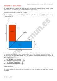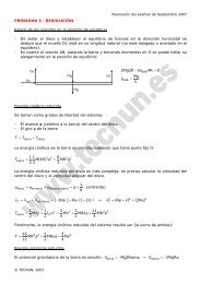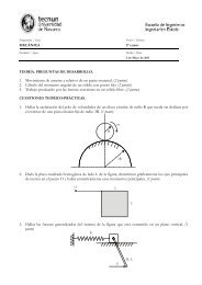
table of contents - Tecnun
table of contents - Tecnun
table of contents - Tecnun
- No tags were found...

Create successful ePaper yourself
Turn your PDF publications into a flip-book with our unique Google optimized e-Paper software.
TABLE OF CONTENTS11.11.21.31.41.51.61.71.81.922.12.22.32.42.52.62.72.8PROPERTIES AND DEFINITIONSOF DIGITAL ICS 1Inverting and Non-Inverting Cates 1Ideal Logic Elements 2Inverter Voltage Transfer Characteristic 4Logic Swing and Transition Width 6Noise in Digital CircuitsFan-In and Fan-Out 76Transient Characteristics 8Power Dissipation 10Power-Delay Product 11DIODES 15PN Junction and MN Schottky Diodes 15Diode Modelling 15Diode CapacitanceSPICE Diode Model1818Diode- Resistor Logic 19Level-Shifted Diode-Resistor Logic 21Clamping Diodes 23Level-Shifting Diodes 243 BIPOLAR JUNCTIONTRANSISTORS3.1 Junction Isolated NPN BJT 273.2 Oxide Isolated NPN BJT 273.3 Multi-Emitter BJT 273.4 Schottky-Clamped BJT 283.5 Lateral PNP BJTs 313.6 The Ebers-Moll BJTModel 313.7 BJTModes <strong>of</strong> Operation 323.8 The Cummel-Poon BJTModel 353.9 SPICE BJTModel 373.10 Integrated Circuit Resistors 394 INTRODUCTION TO BIPOLARDIGITAL CIRCUITS 424.1 Analysis <strong>of</strong> BJT Circuits with KnownStates 424.2 BJTInverter 454.3 TTL Super-Circuitry 464.4 Level-Shifting BJTs 48274.5 Discharge Paths and Base DrivingCircuitry 484.6 Self-Biasing BJTs 494.7 Power Dissipation <strong>of</strong> Bipolar LogicCircuits 505 RESISTOR- TRANSISTORLOGIC (RTL) 565.1 Basic RTL Inverter 565.2 Basic RTL NOR Cate 565.3 Basic RTL NAND Cate 575.4 RTL Fan-Out 595.55.6RTL Power DissipationBasic RTL Non-Inverter62625.7 Basic RTL OR and AND Cates 645.8 RTL with Active Pull-Up 645.9 RTL SPICE Simulation 675.10 Direct Coupled Transistor Logic and CurrentHogging 686 DIODE- TRANSISTOR6.1LOGIC (DTL)Basic DTL Inverter 726.2 Modified DTL 736.3 Transistor Modified DTL 746.4 DTL NAND Cate 756.5 DTL Fan-Out 756.6 DTL Power Dissipation 786.7 DTL SPICE Simulation 807 TRANSISTOR- TRANSISTORLOGIC (TTL) 837.1 Basic TTL Inverter 837.2 Comparison <strong>of</strong> Stored-ChargeDTL and TTL 84Removal from7.3 Basic TTL NAND Cate and the Multiple-Emitter BJT 857.47.5Standard TTL NAND Cate with Totem PoleOutput 85Standard TTL Voltage TransferCharacteristic 877.6 TTL Fan-Out 897.7 TTL Power Dissipation 9172Xl
xiiTable <strong>of</strong> Contents7.8 Open-conector TfL 917.9 Low Power TfL (LTfL) 927.10 High Speed ITL (HTfL) 927.11 TfL SPICE Simulation 938 SCHOTTKY TRANSISTOR-TRANSISTOR LOGIC (STTL)8.1 Schottky-Barrier Diodes 988.2 Schottky-Clamped BJTs 988.3 Schottky-Clamped TfL (STfL) 1018.4 STfL Fan-Out 1048.5 STfL Power Dissipation 1048.6 Low-Power STfL (LSTfL) 1078.7 STfL SPICE Simulation 1109 ADVANCEDSCHOTTKYTRANSISTOR- TRANSISTORLOGIC (ASTTL)9.19.29.3Advanced LSITL (ALSTfL) 115Fairchild Advanced Schottky TfL(FAST) 118Advanced Schottky Transistor-TransistorLogic (ASTfL) 12110 OTHER TTL GA TES10.1 TfL AND Cates 12410.2 TfL NOR Cates 12910.3 TfL OR Cates 13110.4 TfL AND-OR-Invert (AOI) Cates 13310.5 TfL XOR Cates 13710.6 TfL Schmitt Trigger Inverters and NANDCates 14010.7 TfL Tri-State Buffers 14411 BASIC EMITTER-COUPLEDLOGIC(ECL)11.1 BJTCurrent Switch 15511.2 ECL Current Switch Voltage TransferCharacteristic 15611.3 ECL Super-Circuitry 15811.4 Basic ECL NOR/OR Cate 15911512411.5 MECL I NOR/OR Cate with OutputBuffers 16111.611.7MECL I Voltage Transfer CharacteristicMECL I Fan-Out 16316211.8 MECL I Power Dissipation 16511.9 MECL I SPICE Simulation 1679815512 TEMPERA TURECOMPENSA TING EMITTER-COUPLED LOGIC 17112.1 MECL 11with Temperature CompensatingBias Network 17112.2 DC Analysis <strong>of</strong> the Bias Network 17312.3 The Need For TemperatureCompensation 17412.4 Bias Network Compensation for12.5Temperature Variation 176Fan-Out <strong>of</strong> MECL 11 17712.612.7Power Dissipation <strong>of</strong> MECL 11 177MECL 11SPICE Simulation 17913 MECL III and ECL 10K13.1 MECL III 18213.2 MECL III Voltage TransferCharacteristic 18313.3 MECL III Fan-Out 18513.4 MECL III Power Dissipation 18713.5 ECL 10K Series 18913.6 ECL 10K Series SPICE Simulation 18914 MODERN EMITTER-COUPLEDLOGIC14.1 100K ECL Subfamily 19414.2 DC Analysis <strong>of</strong> the 100K ECL BiasNetwork 19614.3 Bias Network Compensation forTemperature Variation 19814.4 Power Dissipation <strong>of</strong> 100K ECLSubfamily 19914.5 Other ECL Families 19915 OTHER ECL GATES15.1 Use <strong>of</strong> NOR/OR Cates as AND/NANDCates with Inverted Inputs 20115.2 conector Dotting Wired-AND Cates 20215.3 conector Dotting Complex OR-AND LogicCates 20615.4 Series Cating-Basic ECL NAND/ANDCurrent Switch 20815.5 Series Cating NAND/AND Cate 21115.6 Series Cating Complex OR-ANDCates 21515.7 ECL XOR/XNOR Cates 21615.8 ECL Decoding Tree 219182194201
Table <strong>of</strong> Contentsxiii16 METAL OXIDESEMICONDUCTOR FIELDEFFECT TRANSISTORS22116.1 Metal Gate N-Channel MOSFETs 22116.2 Silicon Gate N -Channel MOSFETs 22116.3 MOSFET Modes <strong>of</strong> Operation 22116.4 MOSFET Transconductance Parameter 22516.5 MOSFET Threshold Voltage 22616.6 P-Channel MOSFET 22716.7 MOSFET Capacitances 22716.8 SPICE MOSFET Model 22816.9 CMOS Devices 23016.10 Integrated Circuit Capacitors 23217INTRODUCTION TO MOSDIGITAL CIRCUITS17.1 General NMOS Inverter 23417.2 The Zero Drain Current ActiveMOSFET 23417.3 Graphical Solution <strong>of</strong> the NMOSInverter 23717.4 Partial Differentials 23917.5 Analytical Solution <strong>of</strong> the NMOSInverter 24017.617.7Power Dissipation 240MOS Fan-Out 24018 RESISTOR LOADED NMOSINVERTER23424418.1 Operation <strong>of</strong> Resistor Loaded NMOSInverter 24418.2 Graphical Determination <strong>of</strong> VTC for ResistorLoaded NMOS Inverter 24518.3 Calculation <strong>of</strong> VTC Critical Points forResistor Loaded NMOS Inverter 24718.4 Power Dissipation <strong>of</strong> Resistor Loaded NMOSInverter 25018.5 Resistor Loaded NMOS Inverter Dynamic18.6Response 252Resistor Loaded NMOS SPICESimulation 25819 SA TURATED ENHANCEMENT-ONL y LOADED NMOSINVERTER 26119.1 Operation <strong>of</strong> Saturated EIlhancement-OnlyLoaded NMOS Inverter 26119.2 Graphical Determination <strong>of</strong> SaturatedEnhancement-Only Loaded NMOS InverterVTC 26319.3 Calculation <strong>of</strong> VTC Critical Points forSaturated Enhancement-Only LoadedNMOS Inverter 26419.4 Body Bias Considerations for SaturatedEnhancement-Only Loaded NMOSInverter 26619.5 Power Dissipation <strong>of</strong> SaturatedEnhancement-Only Loaded NMOS 27019.6 Saturated Enhancement-Only LoadedNMOS SPICE Simulation 27120LINEAR ENHANCEMENT -ONL yLOADED NMOS INVERTER 27420.1 Operation <strong>of</strong> Linear Enhancemnet-OnlyLoaded NMOS Inverter 27420.2 Graphical Determination <strong>of</strong> LinearEnhancement-Only Loaded NMOS InverterVTC 27620.3 Calculation <strong>of</strong> VTC Critical Points for LinearEnhancement-Only Loaded NMOSInverter 27720.4 Body Bias Consideration for LinearEnhancement-Only Loaded NMOSInverter 28120.5 Power Dissipation <strong>of</strong> Linear Enhancement-Only Loaded NMOS 28420.6 Linear Enhancement-Only Loaded NMOSSPICE Simulation 28521ENHANCEMENT -DEPLETIONLOADED NMOS INVERTER 28821.1 Operation <strong>of</strong> Enhancement-DepletionLoaded NMOS Inverter 28821.2 Graphical Determination <strong>of</strong> Enhancement-Depletion NMOS Inverter VTC 28921.3 Calculation <strong>of</strong> VTC Critical Points forDepletion Loaded NMOS Inverter 29021.4 Body Bias Considerations for Enhancement-Depletion Loaded NMOS Inverter 29421.5 Enhancement-Depletion Loaded NMOSPower Dissipation 29721.6 Enhancement-Depletion Loaded NMOSSPICE Simulation 298
xivTable <strong>of</strong> Contents22 NMOS GATES22.1 NMOS NOR Cate 30322.2 NMOS NAND Cate 30522.3 NMOS OR and AND Cates 30822.4 NMOS Complex Logic Cates (AOIs andOAIs) 30822.5 NMOS XNOR/XOR Logic Cates 31322.622.7NMOS Schmitt Triggers 316NMOS Transmission Cates 323. 30123 CMOS INVERTER 33623.1 Operation <strong>of</strong> ComplementaryInverter 336MOS (CMOS)23.2 Power Dissipation <strong>of</strong> CMOS 33823.3 Craphical DeterminationVTC 339<strong>of</strong> CMOS Inverter23.4 Calculation <strong>of</strong> VTC Critical Points for CMOSInverter 34023.523.6The Symmetric CMOS Inverter 343The Minimum Size CMOS Inverter 34523.7 CMOS Inverter Capacitances 34623.823.9CMOS Inverter Dynamic ResponseCMOS Fan-Out 35834923.10 CMOS Inverter SPICE Simulation 36123.11 Design <strong>of</strong> CMOS Inverters 36423.12 CMOS Latch-Up 36723.13 Electro-Static Discharge and Input ClampingSections 36924CMOS COMBINATIONALLOGIC GATES24.1 CMOS Inverter Pull-Up and Pull-DownReview 37324.2 CMOS NAND Cate 37424.3 CMOS NOR Cate 37924.4 CMOS AND and OR Cates 38424.5 CMOS Complex Logic Cates (AOIs andOAIs) 38424.6 CMOS XOR/XNOR Cates 39937325 CMOS TRI-STATE GATES 41125.1 CMOS Logic Cates with High ImpedanceZ-States 41125.2 CMOS Logic Cates with ContentionX-States 41425.3 CMOS Tri-State (Clocked) Inverters 41725.4 Application <strong>of</strong> Tri-State Inverters 41925.5 Integrated Circuit BUSes Utilizing Tri-StateInverters 42225.6 Ordering <strong>of</strong> Stack Transistors in Tri-StateInverters 42225.7 Tri-State Logic <strong>of</strong> Multi-Input LogicFunctions 42225.8 CMOS Bi-Directional Transmission Cate(Switch) 42625.9 Application <strong>of</strong> CMOS Bi-DirectionalTransmission Cates 43125.10 Disadvantages <strong>of</strong> CMOS Bi-DirectionalTransmission Cates (Non-FaultGradability) 43226CMOS SCHMITT TRIGGERGATES26.1 Hysteresis 43726.2 CMOS Schmitt Inverter 43926.3 Operation and Voltage TransferCharacteristic <strong>of</strong> the CMOS SchmittInverter 44126.4 Design <strong>of</strong> CMOS Schmitt Inverter 44426.5 CMOS Schmitt Inverter with BufferedOutput 44626.6 CMOS Schmitt Inverter with BufferedOutput and Feedback 44726.7 CMOS Schmitt NAND Cates 45143727 CMOS DRIVERS 45327.1 Cascaded CMOS Inverters Driving a LoadCapacitance 45427.2 CMOS Multi-Stage Inverter Drivers 45727.3 CMOS Tri-State Pin Drivers (PadDrivers) 46127.4 Pad Driver with Break-Before-MakeEmbodiment 46328 DYNAMIC CMOS28.1 Pseudo-NMOS Logic 46728.2 CMOS Precharging and Discharging <strong>of</strong> aLoad Capacitance 467283. Dynamic CMOS Logic 46928.4 CMOS Domino Logic 47129COMPARISON ANDINTERFACING OFLOGIC FAMILIES29.1 Comparison <strong>of</strong> Silicon lC LogicFamilies 477467477
Table <strong>of</strong> Contentsxv29.2 Comparison with Callium Arsenide DigitalLogic Families 47829.3 Interfacing Logic Families 47830 BiCMOS48630.1 Reason for BiCMOS 48630.2 BiCMOS Devices 48630.3 BiCMOS Inverters with ResistiveShunts 48830.4 BiCMOS Inverters with Active Shunts 48830.5 BiCMOS Inverters with Parallel OutputCMOS Inverter 48830.6 BiCMOS NAND Cates with ResistiveShunts 49030.7 BiCMOS NAND Cates with ActiveShunts 49130.8 BiCMOS Drivers 49230.9 Full Swing Methods 49431 LATCHES AND FLIP-FLOPS31.1 Basic Definitions for Sequential LogicGates 49831.2 Cross Coupled Inverters 50131.3 Reset-Set (RS) Latch 50431.4 Gated RS Latches 51131.5 Gated RS Latches with Asynchronous Clearand Preset 51331.6 Edge-Triggered Master-Slave RS Flip-Flops 51531.7 JK Latch 52631.8 Edge-Triggered Master-Slave JK Flip-FlopsGKFF) 52831.9 Basic Data (D) Latch 53431.10 Gated Data (D) Latch 53631.11 Tri-State Embodied Cated Data (D)Latches 54031.12 Edge- Triggered Master-Slave DFlip-Flops 54332498SEMI CONDUCTOR READ-ONLyMEMORIES 55632.1 Diode Read-Only Memories 55732.2 BJTRead-Only Memories 56332.3 Bipolar ROM Une Amplifier 57232.4 NMOS NOR Read-Only Memories 57232.5 NMOS NAND Read-Only Memories 58032.6 CMOS Precharging and Discharging <strong>of</strong> aLoad Capacitance 583 .32.7 CMOS Read-Only Memories 58533 SEMI CONDUCTOR STATICRANDOM-ACCESSMEMORIES 60333.1 Static RAM Cell with TransmissionCates 60333.2 MOSFET Static RAM Cell Technologies 60733.3 BJT Static RAM Cell Technologi~s 60834 GALLIUM ARSENIDE METALSEMICONDUCTOR FIELDEFFECT TRANSISTORS 61334.1 N-Channel MESFETs (NMESFETs) 61334.2 Enhancement-Depletion NMESFETs 61534.3 Enhancement-Only NMESFETs 61634.434.5NMESFET Modes <strong>of</strong> OperationNMESFET Transconductance616Parameter 61834.6 NMESFET Threshold Voltage 61834.734.8NMESFET CapacitanceNMESFET Choice 61961934.9 SPICE NMESFET Model 62035DIRECT COUPLED NMESFETLOGIC (DCFL) INVERTER 62235.1 Direct-Coupled Enhancement-OnlyNMESFET Inverters 62235.2 Operation <strong>of</strong> Direct Coupled NMESFETInverter 62235.3 Craphical Determination <strong>of</strong> Direct CoupledInverter VTC 62435.4 Calculation <strong>of</strong> VTC Critical Points for DCFLInverter 62435.5 Optimum 130/I3L0No/WL) Ratio for DCFLInverter 62735.6 Power Dissipation <strong>of</strong> DCFL Inverter 62835.7 DCFL Fan-Out 62835.8 DCFL Inverter SPICE Simulation 62936 SCHOTTKY DIODE NMESFETLOGIC (SDFL) INVERTER 63336.1 SchottkyDiode Enhancement-DepletionInverters 63336.2 Operation <strong>of</strong> SDFLInverter 63336.3 Calculation<strong>of</strong> VTCCriticalVoltagesfor theSDFLInverter 63536.4 Optimum I3D/I3L= WD/WLRatio for SDFLInverter 636
xviTable <strong>of</strong> Contents36.5 Power Dissipation <strong>of</strong> SDFL Inverter 63736.6 SDFL Fan-Out 63836.7 SDFL Inverter SPICE Simulation 63937 BUFFERED NMESFET LOGIC(BFL) INVERTER 64237.1 Buffered Enhancement-Depletion NMESFETInverters 64237.2 Operation <strong>of</strong> BFL Inverter 64237.3 Calculation <strong>of</strong> VTC Critical Voltages for theBFL Inverter 64337.4 Power Dissipation <strong>of</strong> BFL Inverter 64537.5 BFL Fan-Out 64637.6 BFL Inverter SPICE Simulation 64638 OTHER GALLIUM ARSENIDELOGIC FAMILY INVERTERS 64938.1 Capacitar Coupled NMESFET Logic (CCFL)Inverter 64938.2 Capacitar-Diode NMESFET Logic (CDFL)Inverter 64938.3 Source Coupled NMESFET Logic (SCFL)Inverter 65038.4 Low Pinch-Off Voltage NMESFET Logic(LPFL) Inverter 65138.5 Callium Arsenide Transmission Cates 65238.6 Power Dissipation 65339 GALLIUM ARSENIDENMESFET GATES39.1 DCFL NOR Cate 65539.2 DCFL NAND Cate 65639.3 DCFL OR Cate 65765539.4 SDFL NOR Cate 65739.5 SDFL NAND Cate 65839.6 BFL NOR Cate 65939.7 BFL NAND Cate 65939.8 Callium Arsenide NMESFET Complex AND-OR-Invert (AOI) and OR-AND-Invert (OA!)Cates 65939.9 DCFL XOR Cate 66039.10 Other OR/NOR Cates 66139.11 Callium Arsenide Transmission CateLogic 66239.12 Callium Arsenide Static RAM MemoryElements 663APPENDIX AAlA2A3A4DIODE SWITCHINGTIMES 666Development <strong>of</strong> the Stored ChargeEquation 666Shockley's Expression 667Diode Turn-On Transient 668Diode Turn -Off Transient 669APPENDIX BB.1B.2B.3BJT SWITCHINGTIMESDevelopment <strong>of</strong> the Stored ChargeEquation 670BJTTurn-On Transient 670BJTTurn-Off Transient 671SUPPLEMENTARYREADING670672SELECTED ANSWERS674INDEX 679