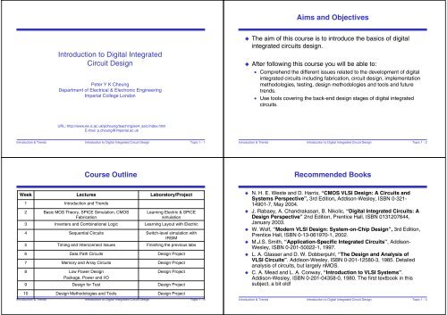
Introduction to Digital Integrated Circuit Design Aims and Objectives ...
Introduction to Digital Integrated Circuit Design Aims and Objectives ...
Introduction to Digital Integrated Circuit Design Aims and Objectives ...
- No tags were found...
You also want an ePaper? Increase the reach of your titles
YUMPU automatically turns print PDFs into web optimized ePapers that Google loves.
Routing a St<strong>and</strong>ard Cell-based ICSt<strong>and</strong>ard Cell LibrariesUse a design kit from the IC vendorBuy an IC-vendor library from a library vendorBuild your own cell libraryRouting a CBIC (cell-based IC)• A “wall” of st<strong>and</strong>ard cells forms a flexible block• metal2 may be used in a feedthrough cell <strong>to</strong> cross over cell rows that usemetal1 for wiring• Other wiring cells: spacer cells, row-end cells, <strong>and</strong> power cells<strong>Introduction</strong> & Trends<strong>Introduction</strong> <strong>to</strong> <strong>Digital</strong> <strong>Integrated</strong> <strong>Circuit</strong> <strong>Design</strong>Topic 1 - 25<strong>Introduction</strong> & Trends<strong>Introduction</strong> <strong>to</strong> <strong>Digital</strong> <strong>Integrated</strong> <strong>Circuit</strong> <strong>Design</strong>Topic 1 - 26Macrocell-Based <strong>Design</strong>Macrocell-Based <strong>Design</strong> ExampleMacrocellInterconnect BusSRAMRouting ChannelSRAMRouting ChannelData pathsSt<strong>and</strong>ard cellsVideo-encoder chip[Brodersen92]<strong>Introduction</strong> & Trends<strong>Introduction</strong> <strong>to</strong> <strong>Digital</strong> <strong>Integrated</strong> <strong>Circuit</strong> <strong>Design</strong>Topic 1 - 27<strong>Introduction</strong> & Trends<strong>Introduction</strong> <strong>to</strong> <strong>Digital</strong> <strong>Integrated</strong> <strong>Circuit</strong> <strong>Design</strong>Topic 1 - 28
Gate-Array–Based ICsGate-Array–Based ICs (con’t)A gate array, masked gate array, MGA, or prediffused array usesmacros (books) <strong>to</strong> reduce turnaround time <strong>and</strong> comprises a basearray made from a base cell or primitive cell. There are three types:• Channeled gate arrays• Channelless gate arrays• Structured gate arraysA channelless gate array (channelfreegate array, sea-of-gates array,or SOG array)• Routing uses rows of unusedtransis<strong>to</strong>rsA channeled gate array• The interconnect uses predefinedspaces between rows of base cellsAn embedded gate array orstructured gate array (mastersliceor masterimage)• Either channeled or channelless• Cus<strong>to</strong>m blocks (the same for eachdesign) can be embedded<strong>Introduction</strong> & Trends<strong>Introduction</strong> <strong>to</strong> <strong>Digital</strong> <strong>Integrated</strong> <strong>Circuit</strong> <strong>Design</strong>Topic 1 - 29<strong>Introduction</strong> & Trends<strong>Introduction</strong> <strong>to</strong> <strong>Digital</strong> <strong>Integrated</strong> <strong>Circuit</strong> <strong>Design</strong>Topic 1 - 30Gate Array Approach - ExamplePrewired ArrayspolysiliconIn1 In2 In3 In4 Categories of prewired arrays (or field-programmabledevices):V DDGNDmetalpossiblecontact• Fuse-based (program-once)• Non-volatile EPROM basedOut• RAM basedUncommitedCellCommittedCell(4-input NOR)<strong>Introduction</strong> & Trends<strong>Introduction</strong> <strong>to</strong> <strong>Digital</strong> <strong>Integrated</strong> <strong>Circuit</strong> <strong>Design</strong>Topic 1 - 31<strong>Introduction</strong> & Trends<strong>Introduction</strong> <strong>to</strong> <strong>Digital</strong> <strong>Integrated</strong> <strong>Circuit</strong> <strong>Design</strong>Topic 1 - 32
Programmable Logic DevicesEPLD Block DiagramPrimary inputsMacrocellPLA PROM PALCourtesy Altera Corp.<strong>Introduction</strong> & Trends<strong>Introduction</strong> <strong>to</strong> <strong>Digital</strong> <strong>Integrated</strong> <strong>Circuit</strong> <strong>Design</strong>Topic 1 - 33<strong>Introduction</strong> & Trends<strong>Introduction</strong> <strong>to</strong> <strong>Digital</strong> <strong>Integrated</strong> <strong>Circuit</strong> <strong>Design</strong>Topic 1 - 34Field-Programmable Gate Arrays Fuse-basedInterconnectI/O BuffersProgrammed interconnectionInput/output pinProgram/Test/DiagnosticsVertical routesCellI/O BuffersI/O BuffersSt<strong>and</strong>ard-cell likefloorplanAntifuseHorizontaltracksRows of logic modulesRouting channelsI/O BuffersVertical tracksProgramming interconnect using anti-fuses<strong>Introduction</strong> & Trends<strong>Introduction</strong> <strong>to</strong> <strong>Digital</strong> <strong>Integrated</strong> <strong>Circuit</strong> <strong>Design</strong>Topic 1 - 35<strong>Introduction</strong> & Trends<strong>Introduction</strong> <strong>to</strong> <strong>Digital</strong> <strong>Integrated</strong> <strong>Circuit</strong> <strong>Design</strong>Topic 1 - 36
Field-Programmable Gate Arrays RAM-basedRAM-based FPGA Basic Cell (CLB)Combinational logicS<strong>to</strong>rage elementsHorizontalroutingchannelCLBCLBswitching matrixInterconnect pointAB/Q1/Q2C/Q1/Q2DAB/Q1/Q2C/Q1/Q2DAny function of up t o4 variablesAny function of up <strong>to</strong>4 variablesRD inFGFGFGRD Q1CERD Q2CEGFCLBCLBEClockCEVertical routing channelCourtesy of Xilinx<strong>Introduction</strong> & Trends<strong>Introduction</strong> <strong>to</strong> <strong>Digital</strong> <strong>Integrated</strong> <strong>Circuit</strong> <strong>Design</strong>Topic 1 - 37<strong>Introduction</strong> & Trends<strong>Introduction</strong> <strong>to</strong> <strong>Digital</strong> <strong>Integrated</strong> <strong>Circuit</strong> <strong>Design</strong>Topic 1 - 38Outline<strong>Design</strong> Abstraction LevelsHis<strong>to</strong>rySYSTEMImplementation methodologies<strong>Design</strong> flow+MODULETechnology scalingGATEVLSI/IC economicsCIRCUITFuture trendsDEVICESn+GDn+<strong>Introduction</strong> & Trends<strong>Introduction</strong> <strong>to</strong> <strong>Digital</strong> <strong>Integrated</strong> <strong>Circuit</strong> <strong>Design</strong>Topic 1 - 39<strong>Introduction</strong> & Trends<strong>Introduction</strong> <strong>to</strong> <strong>Digital</strong> <strong>Integrated</strong> <strong>Circuit</strong> <strong>Design</strong>Topic 1 - 40
ASIC <strong>Design</strong> FlowASIC <strong>Design</strong> Flow (con’t)A design flow is a sequence of steps <strong>to</strong> design an ASIC• <strong>Design</strong> entry.• Logic synthesis.• Pre-layout simulation.• Floorplanning.• Placement.• Routing.• Extraction.• Postlayout simulation.<strong>Introduction</strong> & Trends<strong>Introduction</strong> <strong>to</strong> <strong>Digital</strong> <strong>Integrated</strong> <strong>Circuit</strong> <strong>Design</strong>Topic 1 - 41<strong>Introduction</strong> & Trends<strong>Introduction</strong> <strong>to</strong> <strong>Digital</strong> <strong>Integrated</strong> <strong>Circuit</strong> <strong>Design</strong>Topic 1 - 42OutlineMoore’s LawHis<strong>to</strong>ryImplementation methodologies<strong>Design</strong> flowTechnology scalingVLSI/IC economics In 1965, Gordon Moore, co-founder of Intel, predicted the exponential growth of thenumber of transis<strong>to</strong>rs on an IC (number of transis<strong>to</strong>rs per square inch in ICs <strong>to</strong>double every year) Predicted > 65,000 transis<strong>to</strong>rs by 1975! In subsequent years, the pace slowed down a bit, but density has doubledapproximately every 18 months, <strong>and</strong> this is the current definition of Moore's Law. Growth limited by power Most experts, including Moore himself, expectMoore's Law <strong>to</strong> hold for at least another twodecadesFuture trends<strong>Introduction</strong> & Trends<strong>Introduction</strong> <strong>to</strong> <strong>Digital</strong> <strong>Integrated</strong> <strong>Circuit</strong> <strong>Design</strong>Topic 1 - 43<strong>Introduction</strong> & Trends<strong>Introduction</strong> <strong>to</strong> <strong>Digital</strong> <strong>Integrated</strong> <strong>Circuit</strong> <strong>Design</strong>Topic 1 - 44
Moore’s Law – Intel MicroprocessorsEvolution in ComplexitySource: Intel<strong>Introduction</strong> & Trends<strong>Introduction</strong> <strong>to</strong> <strong>Digital</strong> <strong>Integrated</strong> <strong>Circuit</strong> <strong>Design</strong>Topic 1 - 45<strong>Introduction</strong> & Trends<strong>Introduction</strong> <strong>to</strong> <strong>Digital</strong> <strong>Integrated</strong> <strong>Circuit</strong> <strong>Design</strong>Topic 1 - 46Why ?Scaling Why more transis<strong>to</strong>rs per IC?• Smaller transis<strong>to</strong>rs• Larger dice Why faster computers?• Smaller, faster transis<strong>to</strong>rs• Better microarchitecture• Fewer gate delays per cycle The only constant in VLSI/IC design is constant change Feature size shrinks by 30% every 2-3 years• Transis<strong>to</strong>rs become smaller, faster, less power hungry, cheaper <strong>to</strong>manufacture• Noise, reliability issues1010• Current density goes up63• Wires do not improve1.5(<strong>and</strong> may get worse)S = 2• Typically• Technology nodes Scale fac<strong>to</strong>r SFeature Size (μm)10.11 0.80.60.350.250.180.130.091965 1970 1975 1980 1985 1990 1995 2000 2005Year<strong>Introduction</strong> & Trends<strong>Introduction</strong> <strong>to</strong> <strong>Digital</strong> <strong>Integrated</strong> <strong>Circuit</strong> <strong>Design</strong>Topic 1 - 47<strong>Introduction</strong> & Trends<strong>Introduction</strong> <strong>to</strong> <strong>Digital</strong> <strong>Integrated</strong> <strong>Circuit</strong> <strong>Design</strong>Topic 1 - 48
Scaling ImplicationsPerformance Improvement Improved Performance10,000 Improved Cost1,00040048008 Interconnect Woes Power WoesClock Speed (MHz)100108080808680286Intel386Intel486PentiumPentium Pro/II/III Productivity Challenges1Pentium 4 Physical Limits1970 1975 1980 1985 1990 1995 2000 2005Year<strong>Introduction</strong> & Trends<strong>Introduction</strong> <strong>to</strong> <strong>Digital</strong> <strong>Integrated</strong> <strong>Circuit</strong> <strong>Design</strong>Topic 1 - 49<strong>Introduction</strong> & Trends<strong>Introduction</strong> <strong>to</strong> <strong>Digital</strong> <strong>Integrated</strong> <strong>Circuit</strong> <strong>Design</strong>Topic 1 - 50Cost ImprovementInterconnect WoesIn 2003, $0.01 bought you 100,000 transis<strong>to</strong>rs SIA made a gloomy forecast in 1997• Delay would reach minimum at 250 – 180 nm, then get worsebecause of wires But…• Misleading scale• Global wires 100 kgate blocks ok<strong>Introduction</strong> & Trends<strong>Introduction</strong> <strong>to</strong> <strong>Digital</strong> <strong>Integrated</strong> <strong>Circuit</strong> <strong>Design</strong>Topic 1 - 51<strong>Introduction</strong> & Trends<strong>Introduction</strong> <strong>to</strong> <strong>Digital</strong> <strong>Integrated</strong> <strong>Circuit</strong> <strong>Design</strong>Topic 1 - 52
Reachable RadiusDynamic PowerWe can’t send a signal across a large fast chip in one cycle anymoreBut the microarchitect can plan around this• Just as off-chip memory latencies were <strong>to</strong>leratedChip sizeScaling ofreachable radiusIntel VP Patrick Gelsinger(ISSCC 2001)• If scaling continues atpresent pace, by 2005,high speed processorswould have powerdensity of nuclearreac<strong>to</strong>r, by 2010, arocket nozzle, <strong>and</strong> by2015, surface of sun.• “Business as usual willnot work in the future.”Intel s<strong>to</strong>ck dropped 8% onthe next dayBut attention <strong>to</strong> power isincreasing<strong>Introduction</strong> & Trends<strong>Introduction</strong> <strong>to</strong> <strong>Digital</strong> <strong>Integrated</strong> <strong>Circuit</strong> <strong>Design</strong>Topic 1 - 53<strong>Introduction</strong> & Trends<strong>Introduction</strong> <strong>to</strong> <strong>Digital</strong> <strong>Integrated</strong> <strong>Circuit</strong> <strong>Design</strong>Topic 1 - 54Static PowerProductivityV DD decreases• Save dynamic power• Protect thin gate oxides <strong>and</strong> short channels• No point in high value because of velocity sat.V t must decrease <strong>to</strong>maintain device performanceBut this causes exponentialincrease in OFF leakageMajor future challenge Transis<strong>to</strong>r count is increasing faster than designerproductivity (gates / week)• Bigger design teams Up <strong>to</strong> 500 for a high-end microprocessor• More expensive design cost• Pressure <strong>to</strong> raise productivity Rely on synthesis, IP blocks• Need for good engineering managers<strong>Introduction</strong> & Trends<strong>Introduction</strong> <strong>to</strong> <strong>Digital</strong> <strong>Integrated</strong> <strong>Circuit</strong> <strong>Design</strong>Topic 1 - 55<strong>Introduction</strong> & Trends<strong>Introduction</strong> <strong>to</strong> <strong>Digital</strong> <strong>Integrated</strong> <strong>Circuit</strong> <strong>Design</strong>Topic 1 - 56
Very Few Companies Can <strong>Design</strong> High-End ICsLess First Silicon Success <strong>and</strong> the Changing Rate of Failures10,0001,000Logic transis<strong>to</strong>rs per 100chip10(in millions) 10.10.010.001<strong>Design</strong> productivity gapIC capacityproductivity198119831985198719891991199319951997199920012003200520072009 <strong>Design</strong>er productivity growing at slower rate1981: 100 designer months ~$1M2002: 30,000 designer months ~$300MGap100,00010,0001000100 Productivity(K) Trans./Staff-Mo.1010.1Source: ITRS’990.01Trends are IncreasingLogic/FunctionalNoise / SIPow er ConsumptionClockingFast PathSlow PathAnalog TuningIR DropsYield / ReliabilityFirmw areMixed-SignalInterf aceOtherRET10%28%8%22%13%18%17%16%23%14%9%14%12%10%14%5%4%3%0%45%2003200162% First silicon success rates Betterdeclining• Functional Verification• First Silicon OK48%Noisein/2000SI• 39% Clocking200234% in 2003• IR Drops• Third Silicon OK Worse>90% in 2000• >70% Analog in Tuning 2002•>60%Mixed-Signalin 2003Interface• DFM (RET)Collett International Research:2000, 2002 Functional Verification Studies;2003 <strong>Design</strong> Closure Study, 01/04Trends are Decreasing0% 10% 20% 30% 40% 50% 60% 70%<strong>Introduction</strong> & Trends<strong>Introduction</strong> <strong>to</strong> <strong>Digital</strong> <strong>Integrated</strong> <strong>Circuit</strong> <strong>Design</strong>Topic 1 - 57<strong>Introduction</strong> & Trends<strong>Introduction</strong> <strong>to</strong> <strong>Digital</strong> <strong>Integrated</strong> <strong>Circuit</strong> <strong>Design</strong>Topic 1 - 58Physical LimitsOutlineWill Moore’s Law run out of steam?• Can’t build transis<strong>to</strong>rs smaller than an a<strong>to</strong>m…Many reasons have been predicted for end of scaling• Dynamic power• Subthreshold leakage, tunneling• Short channel effects• Fabrication costs• Electromigration• Interconnect delayRumors of demise have been exaggeratedHis<strong>to</strong>ryImplementation methodologies<strong>Design</strong> flowTechnology scalingVLSI/IC economicsFuture trends<strong>Introduction</strong> & Trends<strong>Introduction</strong> <strong>to</strong> <strong>Digital</strong> <strong>Integrated</strong> <strong>Circuit</strong> <strong>Design</strong>Topic 1 - 59<strong>Introduction</strong> & Trends<strong>Introduction</strong> <strong>to</strong> <strong>Digital</strong> <strong>Integrated</strong> <strong>Circuit</strong> <strong>Design</strong>Topic 1 - 60
Selling price S <strong>to</strong>tal• S <strong>to</strong>tal = C <strong>to</strong>tal / (1-m) m = profit margin<strong>Integrated</strong> <strong>Circuit</strong>s Economics C <strong>to</strong>tal = <strong>to</strong>tal cost• Nonrecurring engineering cost (NRE)• Recurring cost• Fixed costNon-Recurring Engineering Costs (NRE) Engineering cost• Depends on size of design team• Include benefits, training, computers• CAD <strong>to</strong>ols:<strong>Digital</strong> front end: $10KAnalog front end: $100K<strong>Digital</strong> back end: $1M Pro<strong>to</strong>type manufacturing• Mask costs: $500k – 1M in 130 nm process• Test fixture <strong>and</strong> package <strong>to</strong>oling<strong>Introduction</strong> & Trends<strong>Introduction</strong> <strong>to</strong> <strong>Digital</strong> <strong>Integrated</strong> <strong>Circuit</strong> <strong>Design</strong>Topic 1 - 61<strong>Introduction</strong> & Trends<strong>Introduction</strong> <strong>to</strong> <strong>Digital</strong> <strong>Integrated</strong> <strong>Circuit</strong> <strong>Design</strong>Topic 1 - 62Recurring CostsFixed Cost Fabrication• Wafer cost / (Dice per wafer * Yield)• Wafer cost: $500 - $3000• Dice per wafer:2r 2rN = π ⎡⎢ −⎤• Yield: Y = e -ADA⎥⎣ 2A⎦For small A, Y ≈ 1, cost proportional <strong>to</strong> areaFor large A, Y → 0, cost increases exponentially Data sheets <strong>and</strong> application notes Marketing <strong>and</strong> advertising Yield analysis Packaging Test<strong>Introduction</strong> & Trends<strong>Introduction</strong> <strong>to</strong> <strong>Digital</strong> <strong>Integrated</strong> <strong>Circuit</strong> <strong>Design</strong>Topic 1 - 63<strong>Introduction</strong> & Trends<strong>Introduction</strong> <strong>to</strong> <strong>Digital</strong> <strong>Integrated</strong> <strong>Circuit</strong> <strong>Design</strong>Topic 1 - 64
New IC <strong>Design</strong> is Fairly Capital IntensiveCost BreakdownEstimated capital <strong>to</strong> start a company <strong>to</strong> design a wireless communication IC <strong>Digital</strong> designers (7):• $70k salary• $30k overhead• $10k computer• $10k CAD <strong>to</strong>ols• Total: $120k * 7 = $840k Analog designers (3)• $100k salary• $30k overhead• $10k computer• $100k CAD <strong>to</strong>ols• Total: $240k * 3 = $720k Support staff (5)• $45k salary• $20k overhead• $5k computer• Total: $70k * 5 = $350k Fabrication• Back-end <strong>to</strong>ols: $1M• Masks: $1M• Total: $2M / year Summary• 2 years @ $3.91M / year• $8M design & pro<strong>to</strong>typefabbackend <strong>to</strong>ols25%25%salary26%11%9%4%overheadcomputerentry <strong>to</strong>ols<strong>Introduction</strong> & Trends<strong>Introduction</strong> <strong>to</strong> <strong>Digital</strong> <strong>Integrated</strong> <strong>Circuit</strong> <strong>Design</strong>Topic 1 - 65<strong>Introduction</strong> & Trends<strong>Introduction</strong> <strong>to</strong> <strong>Digital</strong> <strong>Integrated</strong> <strong>Circuit</strong> <strong>Design</strong>Topic 1 - 66OutlineEvolution of Intel Microprocessors His<strong>to</strong>ry Implementation methodologies <strong>Design</strong> flow Technology scaling VLSI/IC economics Future trendsIntel Intel Intel Intel Pentium IntelIntel Itanium 8080 4004 486Pentium 286III2IVTransis<strong>to</strong>r Transis<strong>to</strong>r Transis<strong>to</strong>r Transis<strong>to</strong>r count count count count = count = 3,200,000= 221,000,00028,000,000 7,500,000 1,200,000 = 6,000 2,300 = 134,000 42,000,0001971974 198219891993199719992000 2002<strong>Introduction</strong> & Trends<strong>Introduction</strong> <strong>to</strong> <strong>Digital</strong> <strong>Integrated</strong> <strong>Circuit</strong> <strong>Design</strong>Topic 1 - 67<strong>Introduction</strong> & Trends<strong>Introduction</strong> <strong>to</strong> <strong>Digital</strong> <strong>Integrated</strong> <strong>Circuit</strong> <strong>Design</strong>Topic 1 - 68
Intel Microprocessors SummarySilicon in 201010 4 increase in transis<strong>to</strong>r count, clock frequency over 30 years!Die Area: 2.5x2.5 cmVoltage: 0.6 VTechnology:0.07 μmDensity Access Time(Gbits/cm2) (ns)DRAM 8.5 10DRAM (Logic) 2.5 10SRAM (Cache) 0.3 1.5Density Max. Ave. Power Clock Rate(Mgates/cm2) (W/cm2) (GHz)Cus<strong>to</strong>m 25 54 3Std. Cell 10 27 1.5Gate Array 5 18 1Single-Mask GA 2.5 12.5 0.7FPGA 0.4 4.5 0.25<strong>Introduction</strong> & Trends<strong>Introduction</strong> <strong>to</strong> <strong>Digital</strong> <strong>Integrated</strong> <strong>Circuit</strong> <strong>Design</strong>Topic 1 - 69<strong>Introduction</strong> & Trends<strong>Introduction</strong> <strong>to</strong> <strong>Digital</strong> <strong>Integrated</strong> <strong>Circuit</strong> <strong>Design</strong>Topic 1 - 70ITRSSummarySemiconduc<strong>to</strong>r Industry Association forecast• Intl. Technology Roadmap for Semiconduc<strong>to</strong>rs<strong>Integrated</strong> circuits are the faster growing technology the last 45 yearsDifferent implementation methodologies• Trade-off: design <strong>and</strong> turn around time vs design density <strong>and</strong> performanceAbstraction is the basis of design flows <strong>and</strong> <strong>to</strong>olsThe only constant in VLSI design is scaling• Moore’s Law <strong>and</strong> implicationsThe development of integrated circuits requires large investment 32nm in 2013, what next ?<strong>Introduction</strong> & Trends<strong>Introduction</strong> <strong>to</strong> <strong>Digital</strong> <strong>Integrated</strong> <strong>Circuit</strong> <strong>Design</strong>Topic 1 - 71<strong>Introduction</strong> & Trends<strong>Introduction</strong> <strong>to</strong> <strong>Digital</strong> <strong>Integrated</strong> <strong>Circuit</strong> <strong>Design</strong>Topic 1 - 72
Journals <strong>and</strong> ConferencesFurther ReadingIEEE Journal of Solid State <strong>Circuit</strong>sIEICE Transactions on Electronics (Japan)IEEE Transactions on VLSI SystemsOriginal article by MooreArticle on Moore’s LawInternational Solid-State <strong>and</strong> <strong>Circuit</strong>s Conference (ISSCC)VLSI <strong>Circuit</strong>s SymposiumCus<strong>to</strong>m <strong>Integrated</strong> <strong>Circuit</strong>s Conference (CICC)European Solid-State <strong>Circuit</strong>s Conference (ESSCIRC)International ASIC ConferenceInternational Technology Roadmap for Semiconduc<strong>to</strong>rs (2003 Edition,2004 Update)Assignment: Analysis of ITRS 2003 Edition (or 2004 update)<strong>Introduction</strong> & Trends<strong>Introduction</strong> <strong>to</strong> <strong>Digital</strong> <strong>Integrated</strong> <strong>Circuit</strong> <strong>Design</strong>Topic 1 - 73<strong>Introduction</strong> & Trends<strong>Introduction</strong> <strong>to</strong> <strong>Digital</strong> <strong>Integrated</strong> <strong>Circuit</strong> <strong>Design</strong>Topic 1 - 74


