MAX3471 1.6µA, RS-485/RS-422, Half-Duplex, Differential ... - Maxim
MAX3471 1.6µA, RS-485/RS-422, Half-Duplex, Differential ... - Maxim
MAX3471 1.6µA, RS-485/RS-422, Half-Duplex, Differential ... - Maxim
- No tags were found...

You also want an ePaper? Increase the reach of your titles
YUMPU automatically turns print PDFs into web optimized ePapers that Google loves.
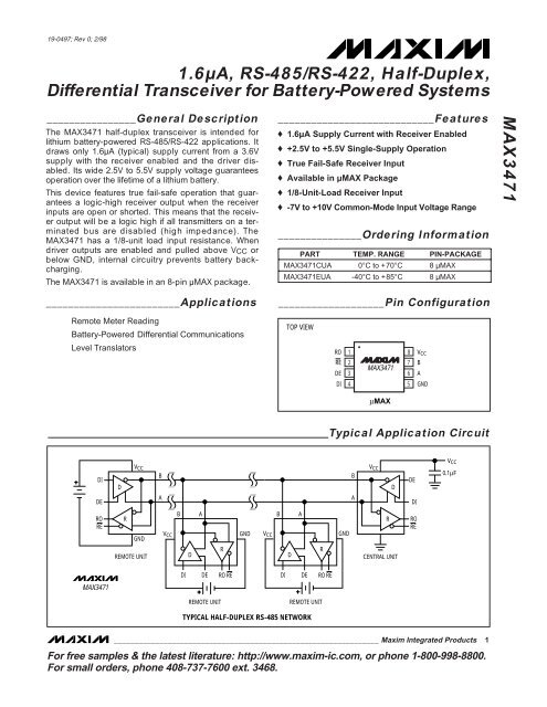
19-0497; Rev 0; 2/98<strong>1.6µA</strong>, <strong>RS</strong>-<strong>485</strong>/<strong>RS</strong>-<strong>422</strong>, <strong>Half</strong>-<strong>Duplex</strong>,<strong>Differential</strong> Transceiver for Battery-Powered Systems________________General DescriptionThe <strong>MAX3471</strong> half-duplex transceiver is intended forlithium battery-powered <strong>RS</strong>-<strong>485</strong>/<strong>RS</strong>-<strong>422</strong> applications. Itdraws only <strong>1.6µA</strong> (typical) supply current from a 3.6Vsupply with the receiver enabled and the driver disabled.Its wide 2.5V to 5.5V supply voltage guaranteesoperation over the lifetime of a lithium battery.This device features true fail-safe operation that guaranteesa logic-high receiver output when the receiverinputs are open or shorted. This means that the receiveroutput will be a logic high if all transmitters on a terminatedbus are disabled (high impedance). The<strong>MAX3471</strong> has a 1/8-unit load input resistance. Whendriver outputs are enabled and pulled above VCC orbelow GND, internal circuitry prevents battery backcharging.The <strong>MAX3471</strong> is available in an 8-pin µMAX package.________________________Applications____________________________Features♦ <strong>1.6µA</strong> Supply Current with Receiver Enabled♦ +2.5V to +5.5V Single-Supply Operation♦ True Fail-Safe Receiver Input♦ Available in µMAX Package♦ 1/8-Unit-Load Receiver Input♦ -7V to +10V Common-Mode Input Voltage Range_______________Ordering InformationPART TEMP. RANGE PIN-PACKAGE<strong>MAX3471</strong>CUA 0°C to +70°C 8 µMAX<strong>MAX3471</strong>EUA -40°C to +85°C 8 µMAX___________________Pin Configuration<strong>MAX3471</strong>Remote Meter ReadingBattery-Powered <strong>Differential</strong> CommunicationsLevel TranslatorsTOP VIEWROREDE123<strong>MAX3471</strong>876V CCBADI45GNDµMAXTypical Application CircuitDIDEDBABAV CCDDEDIV CC0.1µFV CCV CC GNDRORERGNDREMOTE UNITBDARV CCBDARGNDRCENTRAL UNITROREDIDERO REDIDERO RE<strong>MAX3471</strong>REMOTE UNITREMOTE UNITTYPICAL HALF-DUPLEX <strong>RS</strong>-<strong>485</strong> NETWORK________________________________________________________________ <strong>Maxim</strong> Integrated Products 1For free samples & the latest literature: http://www.maxim-ic.com, or phone 1-800-998-8800.For small orders, phone 408-737-7600 ext. 3468.
<strong>1.6µA</strong>, <strong>RS</strong>-<strong>485</strong>/<strong>RS</strong>-<strong>422</strong>, <strong>Half</strong>-<strong>Duplex</strong>,<strong>Differential</strong> Transceiver for Battery-Powered Systems<strong>MAX3471</strong>ABSOLUTE MAXIMUM RATINGS (Note 1)Supply Voltage (V CC ) ..............................................................7VControl Input Voltage (RE, DE)...................-0.3V to (V CC + 0.3V)Driver Input Voltage (DI).............................-0.3V to (V CC + 0.3V)Driver Output/Receiver Input Voltage (A, B).....................±10.5VReceiver Output Voltage (RO)....................-0.3V to (V CC + 0.3V)Continuous Power DissipationµMAX (derate 4.5mW/°C above +70°C) ......................362mWOperating Temperature Ranges<strong>MAX3471</strong>CUA.....................................................0°C to +70°C<strong>MAX3471</strong>EUA ..................................................-40°C to +85°CStorage Temperature Range .............................-65°C to +160°CLead Temperature (soldering, 10sec) .............................+300°CNote 1: All currents into the device are positive; all currents out of the device are negative. All voltages are referred to deviceground unless otherwise noted.Stresses beyond those listed under “Absolute <strong>Maxim</strong>um Ratings” may cause permanent damage to the device. These are stress ratings only, and functionaloperation of the device at these or any other conditions beyond those indicated in the operational sections of the specifications is not implied. Exposure toabsolute maximum rating conditions for extended periods may affect device reliability.DC ELECTRICAL CHARACTERISTICS(V CC = +2.5V to +5.5V, T A = T MIN to T MAX , unless otherwise noted. Typical values are at V CC = +3.6V and T A = +25°C.) (Note 1)PARAMETE<strong>RS</strong>YMBOLCONDITIONSMIN TYP MAXUNITS<strong>Differential</strong> Driver Output (no load)V OD1Figure 1 (R = open)V CCVR = 750Ω (<strong>RS</strong>-<strong>422</strong>)1.5 3.28<strong>Differential</strong> Driver Output(with load)V OD2Figure 1R = 27Ω (<strong>RS</strong>-<strong>485</strong>)R = 27Ω (<strong>RS</strong>-<strong>485</strong>),V CC = 5V, T A = +25°C0.2 0.831.5VChange in Magnitude of<strong>Differential</strong> Output Voltage(Note 2)∆V ODFigure 1, R = 750Ω or 27Ω0.2VDriver Common-Mode OutputVoltageV OCFigure 1, R = 750Ω or 27Ω0.6 x V CCVChange in Magnitude ofCommon-Mode Voltage (Note 2)∆V OCFigure 1, R = 750Ω or 27Ω0.2VInput High VoltageInput Low VoltageDI Input HysteresisInput CurrentInput Current (A and B),<strong>Half</strong> <strong>Duplex</strong>Driver Short-Circuit OutputCurrent (Note 3)Receiver <strong>Differential</strong> ThresholdVoltageReceiver Input HysteresisReceiver Output High VoltageReceiver Output Low VoltageThree-State Current at ReceiverOutputReceiver Input ResistanceV IHV ILV HYSI IN1I IN2I OSDV TH∆V THV OHV OLI OZRR INDE, DI, REDE, DI, REDE, DI, REDE = GND,V CC = GND or 5.5V-7V ≤ V OUT ≤ 10V-7V ≤ V CM ≤ 10VV CM = 0I O = -0.8mA, V ID = -50mVI O = 2.2mA, V ID = -450mVV IN = 10VV IN = -7V -0.075V CC ≤ 3.6V-60 60V CC ≤ 5.5V0.7 x V CC0.3 x V CC100±0.001 ±10.105-130 130-450 -250 -50V CC - 0.40 ≤ V O ≤ V CC ±1 µA-7V ≤ V CM ≤ 10V 96kΩ320.4VVmVµAmAmAmVmVVV2 _______________________________________________________________________________________
<strong>1.6µA</strong>, <strong>RS</strong>-<strong>485</strong>/<strong>RS</strong>-<strong>422</strong>, <strong>Half</strong>-<strong>Duplex</strong>,<strong>Differential</strong> Transceiver for Battery-Powered SystemsDC ELECTRICAL CHARACTERISTICS (continued)(V CC = +2.5V to +5.5V, T A = T MIN to T MAX , unless otherwise noted. Typical values are at V CC = +3.6V and T A = +25°C.) (Note 1)PARAMETERReceiver Output Short-CircuitCurrentSupply CurrentSYMBOLI OSRI CCCONDITIONSMIN TYP MAXV CC ≤ 3.6V-20 500 ≤ V RO ≤ V CCV CC ≤ 5.5V -40 110V CC ≤ 3.6V, no load,RE = DI = GND or V CC ,V A = V B = 0V CC ≤ 5.5V, no load,RE = DI = GND or V CC ,V A = V B = 0UNITSmADE = V CCDE = GND501.6602µADE = V CC83 100DE = GND 2.8 4<strong>MAX3471</strong>SWITCHING CHARACTERISTICS(V CC = +2.5V to +5.5V, T A = T MIN to T MAX , unless otherwise noted. Typical values are at V CC = +3.6V and T A = +25°C.)PARAMETERDriver Input to OutputPropagation DelayDriver Output Skew(t DPLH - t DPHL )Driver Rise or Fall TimeDriver Enable Time to OutputHighDriver Enable Time to OutputLowDriver Disable Time from LowDriver Disable Time from HighReceiver Input to OutputPropagation Delay<strong>Differential</strong> Receiver Skew(t RPLH - t RPHL )Data RateReceiver Enable Time toOutput LowReceiver Enable Time toOutput HighReceiver Disable Time from LowReceiver DisableTime from HighSYMBOLCONDITIONSMIN TYP MAXt DPLH, Figures 3 and 5, R DIFF = 1.5kΩ,1.40 2.00t DPHL C L1 = C L2 = 100pFt DSKEWt DR , t DFt DZHt DZLFigures 3 and 5, R DIFF = 1.5kΩ,C L1 = C L2 = 100pFFigures 3 and 5, R DIFF = 1.5kΩ,C L1 = C L2 = 100pF0.0250.75 1.34 1.75UNITSFigures 4 and 6, C L = 100pF, S2 closed, S1 open 1.5 6.00 µsFigures 4 and 6, C L = 100pF, S1 closed, S2 open 0.86 4.00 µst DLZ Figures 4 and 6, C L = 15pF, S1 closed, S2 open 0.4 1.5 µst DHZ Figures 4 and 6, C L = 15pF, S2 closed, S1 open 0.6 1.5 µst RPLH 5.2 12Figures 7 and 9, C L = 15pF, |V ID| = 2Vt RPHL6.4 12µst <strong>RS</strong>KEWf MAXt RZLt RZHt RLZt RHZFigures 7 and 9, |V ID| = 2V 1.2µsFigure 9, C L = 100pFFigures 2 and 8, C L = 15pF, S1 closed, S2 openFigures 2 and 8, C L = 15pF, S2 closed, S1 openFigures 2 and 8, C L = 15pF, S1 closed, S2 openFigures 2 and 8, C L = 15pF, S2 closed, S1 open6470 50085 50050 20035 200µsµsµskbpsnsnsnsnsNote 1: All currents into the device are positive; all currents out of the device are negative. All voltages are referred to deviceground unless otherwise noted.Note 2: ∆V OD and ∆V OC are the changes in magnitude of V OD and V OC , respectively, when the DI input changes state.Note 3: <strong>Maxim</strong>um and minimum current levels apply to peak current just prior to foldback-current limiting._______________________________________________________________________________________ 3
<strong>1.6µA</strong>, <strong>RS</strong>-<strong>485</strong>/<strong>RS</strong>-<strong>422</strong>, <strong>Half</strong>-<strong>Duplex</strong>,<strong>Differential</strong> Transceiver for Battery-Powered Systems<strong>MAX3471</strong>__________________________________________Typical Operating Characteristics(V CC = +3.6V, T A = +25°C, unless otherwise noted.)OUTPUT CURRENT (mA)454035302520151050OUTPUT CURRENTvs. RECEIVER OUTPUT LOW VOLTAGEV CC = 5VV CC = 3.6V0 0.2 0.4 0.6 0.8 1.0 1.2 1.4 1.6 1.8 2.0OUTPUT LOW VOLTAGE (V)<strong>MAX3471</strong>toc01OUTPUT CURRENT (mA)20181614121086420OUTPUT CURRENT vs. RECEIVEROUTPUT HIGH VOLTAGEV CC = 3.6VV CC = 5V0 0.5 1.0 1.5 2.0 2.5 3.0 3.5 4.0 4.5 5.0OUTPUT HIGH VOLTAGE (V)<strong>MAX3471</strong>toc02RECEIVER OUTPUT VOLTAGE (V)5.55.04.54.03.53.0RECEIVER OUTPUT HIGHVOLTAGE vs. TEMPERATURELOAD = 0.8mAV CC = 5VV CC = 3.6V-50 -25 0 25 50 75 100 125TEMPERATURE (°C)<strong>MAX3471</strong>toc03RECEIVER OUTPUT VOLTAGE (mV)140120100806040200RECEIVER OUTPUT LOWVOLTAGE vs. TEMPERATURELOAD = 2.2mAV CC = 3.6VV CC = 5V-50 -25 0 25 50 75 100 125TEMPERATURE (°C)<strong>MAX3471</strong>toc04DRIVER OUTPUT CURRENT (mA)4035302520151050DRIVER OUTPUT CURRENTvs. DIFFERENTIAL OUTPUT VOLTAGEV CC = 3.6VV CC = 5V0 0.5 1.0 1.5 2.0 2.5 3.0 3.5 4.0 4.5 5.0DIFFERENTIAL OUTPUT VOLTAGE (V)<strong>MAX3471</strong>toc05DIFFERENTIAL OUTPUT VOLTAGE (V)2.01.81.61.41.21.00.80.60.4DRIVER DIFFERENTIALOUTPUT VOLTAGE vs. TEMPERATUREV CC = 5VV CC = 3.6V0.2R DIFF = 54Ω0-50 -25 0 25 50 75 100 125TEMPERATURE (°C)<strong>MAX3471</strong>toc06DIFFERENTIAL OUTPUT VOLTAGE (V)5.04.54.03.53.02.52.01.51.0DRIVER DIFFERENTIALOUTPUT VOLTAGE vs. TEMPERATUREV CC = 5VV CC = 3.6V0.5R DIFF = 1.5kΩ0-50 -25 0 25 50 75 100 125TEMPERATURE (°C)<strong>MAX3471</strong>toc07OUTPUT CURRENT (mA)6050403020100OUTPUT CURRENT vs. DRIVEROUTPUT LOW VOLTAGE (V CC = 5V)V CC = 5V0 1 2 3 4 5 6 7 8 9 10OUTPUT LOW VOLTAGE (V)<strong>MAX3471</strong>toc08OUTPUT CURRENT (mA)302520151050OUTPUT CURRENT vs. DRIVEROUTPUT LOW VOLTAGE (V CC = 3.6V)V CC = 3.6V0 2 4 6 8 10 12OUTPUT LOW VOLTAGE (V)<strong>MAX3471</strong>toc094 _______________________________________________________________________________________
<strong>1.6µA</strong>, <strong>RS</strong>-<strong>485</strong>/<strong>RS</strong>-<strong>422</strong>, <strong>Half</strong>-<strong>Duplex</strong>,<strong>Differential</strong> Transceiver for Battery-Powered SystemsTypical Operating Characteristics (continued)(V CC = +3.6V, T A = +25°C, unless otherwise noted.)OUTPUT CURRENT (mA)454035302520151050OUTPUT CURRENT vs. DRIVEROUTPUT HIGH VOLTAGE (V CC = 5V)V CC = 5V-12 -10 -8 -6 -4 -2 0 2 4 6OUTPUT HIGH VOLTAGE (V)<strong>MAX3471</strong>toc10OUTPUT CURRENT (mA)2520151050OUTPUT CURRENT vs. DRIVEROUTPUT HIGH VOLTAGE (V CC = 3.6V)V CC = 3.6V-12 -10 -8 -6 -4 -2 0 2 4OUTPUT HIGH VOLTAGE (V)<strong>MAX3471</strong>toc11SUPPLY CURRENT (µA)9080706050403020100NO-LOAD SUPPLY CURRENTvs. TEMPERATURE (DE = V CC )V CC = 5.5VV CC = 5.0VV CC = 3.6VV CC = 2.5VDE = V CC-50 -25 0 25 50 75 100 125TEMPERATURE (°C)<strong>MAX3471</strong>toc12<strong>MAX3471</strong>SUPPLY CURRENT (µA)3.02.52.01.51.00.50NO-LOAD SUPPLY CURRENTvs. TEMPERATURE (DE = GND)V CC = 5.5VV CC = 5.0VV CC = 3.6VV CC = 2.5VDE = GND-50 -25 0 25 50 75 100 125TEMPERATURE (°C)<strong>MAX3471</strong>toc13PROPAGATION DELAY (µs)1.51.41.31.21.11.00.90.80.7DRIVER PROPAGATION DELAY(t DPHL , t DPLH ) vs. TEMPERATUREV CC = 3.6V, R DIFF = 1.5kΩV CC = 5V, R DIFF = 1.5kΩV CC = 5V, R DIFF = 54ΩC L1 = C L2 = 100pFV CC = 3.6V, R DIFF = 54Ω-40 -20 0 20 40 60 80 100TEMPERATURE (°C)<strong>MAX3471</strong>toc14PROPAGATION DELAY (µs)6543210RECEIVER PROPAGATIONDELAY (t PLH ) vs. TEMPERATUREV CC = 3.6VCIRCUIT OF FIGURE 9C L = 100pF|V ID | = 2VV CC = 5V-40 -20 0 20 40 60 80 100TEMPERATURE (°C)MAS3471toc15PROPAGATION DELAY (µs)7.57.06.56.05.55.04.54.03.53.0RECEIVER PROPAGATIONDELAY (t PHL ) vs. TEMPERATUREV CC = 3.6VV CC = 5V|V ID | = 2VC L = 100pF-40 -20 0 20 40 60 80 100TEMPERATURE (°C)<strong>MAX3471</strong>toc16_______________________________________________________________________________________ 5
<strong>1.6µA</strong>, <strong>RS</strong>-<strong>485</strong>/<strong>RS</strong>-<strong>422</strong>, <strong>Half</strong>-<strong>Duplex</strong>,<strong>Differential</strong> Transceiver for Battery-Powered Systems<strong>MAX3471</strong>Typical Operating Characteristics (continued)(V CC = +3.6V, T A = +25°C, unless otherwise noted.)RECEIVER PROPAGATION DELAY<strong>MAX3471</strong>toc17B(2V/div)ADI(2V/div)DRIVER PROPAGATION DELAY<strong>MAX3471</strong>toc18A(2V/div)BDI(2V/div)A-B(2V/div)R O(2V/div)A-B(1V/div)1µs/div400ns/divR = 1.5kΩ, C L = 100pF______________________________________________________________Pin DescriptionPIN12345678NAMEROREDEDIGNDABV CCReceiver Output. When RE is low, if A - B ≥ -50mV, RO will be high; if A - B ≤ -450mV, RO will be low.Receiver Output Enable. Drive RE low to enable RO; RO is high impedance when RE is high.Driver Output Enable. Drive DE high to enable the driver outputs. These outputs are high impedance whenDE is low.Driver Input. With DE high, a low on DI forces the noninverting output low and the inverting output high.Similarly, a high on DI forces the noninverting output high and the inverting output low.GroundNoninverting Driver Output and Noninverting Receiver InputInverting Driver Output and Inverting Receiver InputPositive Supply: +2.5V ≤ V CC ≤ +5.5VFUNCTION_______________Detailed DescriptionThe <strong>MAX3471</strong> half-duplex transceiver consumes only<strong>1.6µA</strong> from a single +3.6V supply. Its wide 2.5V to 5.5Vsupply voltage guarantees operation over the lifetime ofa lithium battery. This device contains one driver andone receiver. Its true fail-safe receiver input guaranteesa logic-high receiver output when the receiver inputsare open or shorted, or when they are connected to aterminated transmission line with all drivers disabled.Reduced-slew-rate drivers minimize EMI and reducereflections caused by improperly terminated cables,allowing error-free data transmission up to 64kbps.Receiver Input FilteringThe <strong>MAX3471</strong> receiver operates at up to 64kbps andincorporates input filtering in addition to input hysteresis.This filtering enhances noise immunity when differentialsignals have very slow rise and fall times.The <strong>MAX3471</strong> guarantees a logic-high receiver outputwhen the receiver inputs are shorted or open, or whenthey are connected to a terminated transmission linewith all drivers disabled. This is accomplished by settingthe receiver threshold between -50mV and-450mV. If the differential receiver input voltage (A-B) isgreater than or equal to -50mV, RO is a logic high. IfA-B is less than or equal to -450mV, RO is a logic low.In the case of a terminated bus with all transmitters disabled,the receiver’s differential input voltage is pulledto 0V by the termination. With the <strong>MAX3471</strong>’s receiverthresholds, this results in a logic high with a 50mV minimumnoise margin.6 _______________________________________________________________________________________
<strong>1.6µA</strong>, <strong>RS</strong>-<strong>485</strong>/<strong>RS</strong>-<strong>422</strong>, <strong>Half</strong>-<strong>Duplex</strong>,<strong>Differential</strong> Transceiver for Battery-Powered SystemsTable 1. TransmittingINPUTSOUTPUTSRE DE DI B AX 1 1 01X 1 0 100 0 X Z D Z D1 0 X Z D Z DZ D = Driver output disabledTable 2. Receiving0 010INPUTSRE DE A-BRO0 0 ≥ -0.05V1≤ -0.45V0 0 Open/Shorted1X = Don’t careZ = Receiver output high impedanceXOUTPUT0Z<strong>MAX3471</strong>__________ Applications InformationTransceivers on the BusThe <strong>MAX3471</strong> is optimized for the unterminated busnormally used in slow, low-power systems. Witha +2.5V supply, the part is guaranteed to drive up toeight standard loads (for example, 64 other <strong>MAX3471</strong>s or56 <strong>MAX3471</strong>s plus one standard load). Drive capabilityincreases significantly with supply. For example, witha +5V supply, the <strong>MAX3471</strong> typically meets the <strong>RS</strong>-<strong>485</strong>driver output specifications (1.5V with 54Ω differential termination).See the Typical Operating Characteristics.ABRRReduced EMI and ReflectionsThe <strong>MAX3471</strong> is slew-rate limited, minimizing EMI andreducing reflections caused by improperly terminatedcables. In general, the rise time of a transmitter directlyrelates to the length of an unterminated stub, which canbe driven with only minor waveform reflections. The followingequation expresses this relationship conservatively:Length = t RISE / (10 x 1.5ns/foot)where t RISE is the transmitter’s rise time.For example, the <strong>MAX3471</strong>’s rise time is typically 1.3µs,which results in excellent waveforms with a stub lengthup to 82 feet. In general, systems operate well withlonger unterminated stubs, even with severe reflections,if the waveform settles out before the UART samplesthem.Driver Output ProtectionExcessive output current and power dissipation causedby faults or bus contention are prevented by foldbackcurrent limiting. A foldback current limit on the outputstage provides immediate protection against short circuitsover the whole common-mode voltage range (seeTypical Operating Characteristics).Figure 1. Driver DC Test LoadRECEIVEROUTPUTTESTPOINT1kS1V ODV OCDEV CCDIV CCR DIFFC L1DRIVERAV OC LS2BC L2Figure 2. Receiver Enable/Disable Timing Test LoadFigure 3. Driver Test Circuit_______________________________________________________________________________________ 7
<strong>1.6µA</strong>, <strong>RS</strong>-<strong>485</strong>/<strong>RS</strong>-<strong>422</strong>, <strong>Half</strong>-<strong>Duplex</strong>,<strong>Differential</strong> Transceiver for Battery-Powered Systems<strong>MAX3471</strong>OUTPUTUNDER TESTC L12kS1S2V CCV CCDI0VBAV DIFF-V OV O0VV CC2V O1/2 V Ot DPLHt DPHLV DIFF = V (A) - V (B)V CC21/2 V O90% 90%10% 10%t DRt DSKEW = (t DPLH - t DPHL )t DFFigure 4. Driver Enable/Disable Timing Test LoadFigure 5. Driver <strong>Differential</strong> Propagation Delay and Rise/Fall TimesV CCDE0VV CC2V CC2V TESTV CCA, B2OUTPUT NORMALLY LOW V OL + 0.5VV OH OUTPUT NORMALLY HIGHV OLA, BV CCV OH - 0.5V0V2t DZH t DHZV TEST = 0.91V CCt DZLt DLZV OHR OV OLABt RPHL|V ID | = 2Vt <strong>RS</strong>KEW = (t RPLH = t RPHL )1.4V OUTPUT 1.4Vt RPLHINPUTFigure 6. Driver Enable and Disable TimesFigure 7. Receiver Propagation DelayV CCRE0VV CC2t RZLt RLZV CCROV OLV OH1.4VOUTPUT NORMALLY LOWOUTPUT NORMALLY HIGHV OL + 0.5VROV OH - 0.5V0V1.4Vt RZH t RHZFigure 8. Receiver Enable and Disable TimesV CC2V IDBARECEIVERREC LRECEIVEROUTPUTFigure 9. Receiver Propagation Delay and <strong>Maxim</strong>um Data-Rate Test Circuit___________________Chip InformationTRANSISTOR COUNT: 351<strong>Maxim</strong> cannot assume responsibility for use of any circuitry other than circuitry entirely embodied in a <strong>Maxim</strong> product. No circuit patent licenses areimplied. <strong>Maxim</strong> reserves the right to change the circuitry and specifications without notice at any time.8 _____________________<strong>Maxim</strong> Integrated Products, 120 San Gabriel Drive, Sunnyvale, CA 94086 408-737-7600© 1998 <strong>Maxim</strong> Integrated Products Printed USA is a registered trademark of <strong>Maxim</strong> Integrated Products.