ECE 4670 Spring 2011 Lab 5 Frequency Modulation, Demodulation ...
ECE 4670 Spring 2011 Lab 5 Frequency Modulation, Demodulation ...
ECE 4670 Spring 2011 Lab 5 Frequency Modulation, Demodulation ...

Create successful ePaper yourself
Turn your PDF publications into a flip-book with our unique Google optimized e-Paper software.
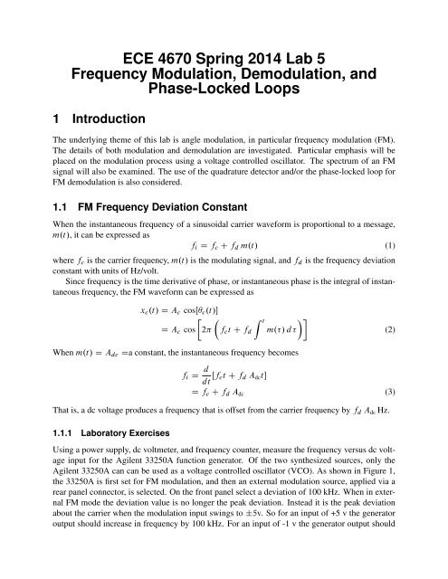
<strong>ECE</strong> <strong>4670</strong> <strong>Spring</strong> 2014 <strong>Lab</strong> 5<strong>Frequency</strong> <strong>Modulation</strong>, <strong>Demodulation</strong>, andPhase-Locked Loops1 IntroductionThe underlying theme of this lab is angle modulation, in particular frequency modulation (FM).The details of both modulation and demodulation are investigated. Particular emphasis will beplaced on the modulation process using a voltage controlled oscillator. The spectrum of an FMsignal will also be examined. The use of the quadrature detector and/or the phase-locked loop forFM demodulation is also considered.1.1 FM <strong>Frequency</strong> Deviation ConstantWhen the instantaneous frequency of a sinusoidal carrier waveform is proportional to a message,m.t/, it can be expressed asf i D f c C f d m.t/ (1)where f c is the carrier frequency, m.t/ is the modulating signal, and f d is the frequency deviationconstant with units of Hz/volt.Since frequency is the time derivative of phase, or instantaneous phase is the integral of instantaneousfrequency, the FM waveform can be expressed asx c .t/ D A c cosŒ c .t/ Z tD A c cos 2 f c t C f d m./ d(2)When m.t/ D A dc Da constant, the instantaneous frequency becomesf i D d dt Œf ct C f d A dc tD f c C f d A dc (3)That is, a dc voltage produces a frequency that is offset from the carrier frequency by f d A dc Hz.1.1.1 <strong>Lab</strong>oratory ExercisesUsing a power supply, dc voltmeter, and frequency counter, measure the frequency versus dc voltageinput for the Agilent 33250A function generator. Of the two synthesized sources, only theAgilent 33250A can can be used as a voltage controlled oscillator (VCO). As shown in Figure 1,the 33250A is first set for FM modulation, and then an external modulation source, applied via arear panel connector, is selected. On the front panel select a deviation of 100 kHz. When in externalFM mode the deviation value is no longer the peak deviation. Instead it is the peak deviationabout the carrier when the modulation input swings to ˙5v. So for an input of +5 v the generatoroutput should increase in frequency by 100 kHz. For an input of -1 v the generator output should
1.2 FM <strong>Modulation</strong> Index - ˇ6781-+*#99:$%6?3B&"",-CD*-)+01A@6781-+*#99
1.2 FM <strong>Modulation</strong> Index - ˇ=*7D&EFD==.>(=.>(1&%#9='8)0138B)C?>@='8)&%)90A23(B)CNGB9)C=.>(!%&'()&*+,789:'%$;)0(GB9)C=.>(1GB9)C=.>(109B9)C"%.>(H!"#$%I32IE"G.#J)1K'I1)LI,22M!+O!+O1UV012K23456-.)/013?56G0QRS;J8%#T H2M*#$%0A23OP8%(7?$0&2@$706A*,>2(*1$B$C$D$*+$,/*1$E71(!"#$%E"G.#J)E"G.#J)1**,*0A23OP8!"#$%&'()$*+,&$-.$&/01$*1$.$230/()(4$,/($5$6/71($1/*8,19:$;.$2(,$*1=!------------ "#= ! &8$+&$E&+E()+$/()("#Figure 3: ADS simulation schematic.%""$""#""123.(,-*1!"""'!""'#""'$""'%""" !" #" $" %"&"()*+,-./+0Figure 4: ADS FM output waveform.<strong>ECE</strong> <strong>4670</strong> <strong>Lab</strong> 5 5
1.3 FM with Other than Sinusoidal Signals!'$!:;?9'&!'*!')!'(!'+!!"% !"# $"! $"$$"&,-./0.123456789Figure 5: ADS FM spectrum with ˇ D 3.swing in carrier frequency from its unmodulated value. The bandwidth occupied by an FMsignal is related to the peak deviation, but not in rigorous fashion. Set the peak deviation,f d A m D f , at a fixed value that gives sidebands out to about 100 kHz on each side of thecarrier (use about 50 kHz per division on the analyzer).7. Decrease the modulating frequency without changing f , and notice the effect on the spectrum.Measure the bandwidth at several different modulating frequencies. If you are usingthe 10dB per division vertical scale you can define spectral bandwidth in terms of the frequenciesfor which the spectrum is say 10 or 20dB down from its peak value. Calculatethe relationship between f and bandwidth for each. Carson’s rule for FM by a sinusoidalsignal of frequency f m states that the bandwidth is approximatelyWould you agree with this approximation?1.3 FM with Other than Sinusoidal SignalsBW D 2 f m .ˇ C 1/ D 2.f C f m / (6)The Fourier series (or transform) for an FM waveform is mathematically tractable for only a fewspecial cases, the sinusoidal case being one of them. For signals which are more complicated,the detailed structure of the spectrum cannot be analyzed. Only a few rules relating modulatingfrequency, bandwidth, and peak deviation can be used to describe the frequency domain representationof FM for the general case.<strong>ECE</strong> <strong>4670</strong> <strong>Lab</strong> 5 6
1.3 FM with Other than Sinusoidal Signals:;?9!'$!'&!'*!')!?$@-./A$"!!!678$!BC;D$!5:EF.2G-H1$9I*!A'$&")%!?$!"#$%&"'$()*#+&),(-..'/-&*011-%'(!'+!!"% !"# $"! $"$$"&,-./0.123456789Figure 6: ADS spectrum with ˇ such that the third sideband is nulled.<strong>ECE</strong> <strong>4670</strong> <strong>Lab</strong> 5 7
1.3 FM with Other than Sinusoidal SignalsSuppose m.t/ is a zero average value square wave of amplitude ˙A m . Then the instantaneousfrequency of the resulting FM signal jumps from .f c f d A m / to .f c C f d A m / or from .f c f /to .f c C f /. Mathematically we can write this as1Xx c .t/ D p.t nT m / (7)wherenD 1 t Tm =4p.t/ D A c…cosŒ2.f c C f /tT m =2 t 3Tm =4C …cosŒ2.f c f /tT m =2For this special case the power spectral density of x c .t/ is relatively easy to obtain. Clearly S x .f /will consist of delta functions spaced at multiples of 1=T m . The envelope of S x .f / is proportionalto jP.f /j 2 .1.3.1 <strong>Lab</strong>oratory Exercises1. Using the Agilent 33250A function generator with a carrier frequency of 1 MHz, apply asquare wave signal of 10 kHz to the v mod input. The test set-up is shown in Figure 7.(8)6781-+*#99:$%6?3B&"",-CD*-)+01A@6781-+*#99
1.4 FM <strong>Demodulation</strong>3. Observe the spectrum on the analyzer as f is increased. Use the analyzer with zero frequencyin the center and with 500 kHz per division so that both positive and “negative”frequencies can be observed. Compare your measured results to ADS simulation resultssimilar that shown in Figures 8 and 9.+,-.+,-./Q%#(+8B)0/3B')*J-V+8B)Q%)(0@43.')*ABFigure 8: ADS simulation schematic for squarewave FM.4. Slowly increase and decrease the modulation amplitude. Notice that at high levels the spectrumseems to cross the zero frequency line.5. Return the 33250A frequency deviation back to 100 kHz as in Section 1.1.1. Set the amplitudefor a ˙100 kHz bandwidth and decrease the modulation frequency without changingf . Does Carson’s rule seem to hold for this signal?6. Use an FM radio for a voice/music signal to modulate the 33250A generator. Set the bandwidthat about ˙100 kHz for this “random” signal and observe the spectrum. Manuallyincrease the analyzer sweep speed so that you can more clearly see the constant changes inthe spectral picture for this general case.1.4 FM <strong>Demodulation</strong>To recover the information contained in an FM signal requires obtaining the signals instantaneousfrequency. For the signal Z tx c .t/ D A c cosŒ! c t C .t/ D A c cos ! c t C k f m.˛/ d˛(9)the instantaneous radian frequency is! i .t/ D ! c C d.t/dtD ! c C k f m.t/ (10)<strong>ECE</strong> <strong>4670</strong> <strong>Lab</strong> 5 9
1.4 FM <strong>Demodulation</strong>$!!($!>$?,-.@ $"$!!567$!AB:C$!49DE-1F,G0$8H*!@(&"$!I>$!"#$%&#'()*+,-.,'%/0123,)0'4)1,52")6789#:)6;;)
1.4 FM <strong>Demodulation</strong>where k f D 2f d . The ideal FM discriminator, shown in Figure 10, produces outputy D .t/ D 12 K d.t/DdtD K D f d m.t/: (11)Practical implementation of the ideal FM discriminator can be done using analog circuit designor using digital signal processing. In this part of the lab we will consider the use of an analog phaselockedloop (PLL) with sinusoidal phase detector, as shown in Figure 11, for FM demodulation.For modeling purposes we let# $ %$%&'()*(+(,+-.& ' %!" & ! %!"#& ( %Figure 11: General PLL diagram employing a sinusoidal phase detector.x r .t/ D A c sin 2f c t C .t/ (12)e o .t/ D A v cos 2f c t C O .t/ : (13)Note that frequency error may also be included in .t/ D .t/frequency term is removed, we can writeO .t/. Assuming the doublee d .t/ D 1 2 A cA v K d sin .t/ O .t/: (14)The VCO, see Figure 12, converts voltage to frequency deviation relative the VCO quiescent frequencyf 0 . The VCO output instantaneous frequency in Hz isf VCO .t/ D f 0 C K v2 e v.t/ D f 0 C 12 d .t/ O : (15)dte v () tVCOK vA v cos[ ω 0 t + θˆ () t ]Figure 12: VCO model.The frequency deviation in radians/s isVCO <strong>Frequency</strong> Deviation D d O .t/dtD K v e v .t/ (16)<strong>ECE</strong> <strong>4670</strong> <strong>Lab</strong> 5 11
1.4 FM <strong>Demodulation</strong>In mathematical terms we now close the loop by connecting the phase detector output to the VCOthrough a convolution of the loop filter impulse responsed.t/O D A ZcA v K d K tvf .t / sin ./ ./ O d (17)dt 2This equation can be represented in block diagram form as the nonlinear feedback control modelof Figure 13. %" %&"#$! ' & " !------------------- (%!$# ) " %ˆ %!----- "#Figure 13: Non-linear baseband PLL model.When the loop is in lock, with small phase error, i.e.sinŒ.t/ D sinŒ.t/ O .t/ ' .t/ O .t/ D .t/; (18)we can linearize the loop. This linearizing leads to the s-domain PLL model shown in Figure 14.Working from the block diagram we can solve for ‚.s/ in terms of ˆ.s/ ("! (% & % " !------------------- '!$# ) " (ˆ (!----- "#Figure 14: Linear baseband PLL model.whereor O‚.s/ 1 C K ts F .s/O‚.s/ D K t ‚.s/sO‚.s/ F .s/D K t‚.s/F .s/; (19)sK t D 1 2 A cA v K d K v / rad/s (20)Finally, the closed-loop transfer function, H.s/ D O‚.s/=‚.s/, can be written asH.s/ D O ‚.s/‚.s/ DK tF .s/s C K t F .s/ : (21)<strong>ECE</strong> <strong>4670</strong> <strong>Lab</strong> 5 12
1.4 FM <strong>Demodulation</strong>For a first-order PLL F .s/ D 1, then we haveH.s/ DK ts C K t(22)We are finally in a position to consider the details of how the first-order PLL recovers the FMmessage signal m.t/. With FM the phase deviation at the PLL input (from the FM transmitter) iswhere M.s/ D Lfm.t/g. The VCO control voltage input is‚.s/ D f dM.s/; (23)sE v .s/ D ‚.s/ D k vM.s/sD f dK vsK v H.s/sK vK ts C K tK t M.s/: (24)s C K tThe 3dB bandwidth in Hz of the FM demodulator is just the loop gain divided by 2Demodulator 3dB Bandwidth D K t2Hz (25)The linear analysis assumes that the loop is in lock. The first-order PLL is in lock if d O .t/=dt D0. The governing relationship for the loop to be in lock is the nonlinear differential equation of(17). For the case of the first-order loop we haved O .t/dtD K t sinŒ.t/: (26)Suppose the loop is in lock for t < 0 and the input phase deviation undergoes a step change infrequency, i.e.,d.t/D ! u.t/; (27)dtwhere we assume ! > 0. Combining this with (26), we can writed.t/dtD ! u.t/ K t sinŒ.t/: (28)A plot of d.t/=dt versus .t/ is known as the phase plane plot. The phase plane plot for afirst-order PLL having ! > 0 is shown in Figure 15. At t D 0 the phase plane operating pointjumps to d.t/=dtj tD0 D !. Since dt is also positive, we conclude that d is also positive.If d.t/=dt should become negative d is also negative, which drives the operating point to thestable lock point which again has d.t/=dt D 0 (a frequency error of zero). Due to the finiteloop gain, K t , there is a steady-state phase error ss when the loop finally settles. We conclude thatfor the loop to lock, or in this case remain locked, the phase plane curve must cross the d=dt D 0axis.<strong>ECE</strong> <strong>4670</strong> <strong>Lab</strong> 5 13
1.4 FM <strong>Demodulation</strong>d------------ tdt – K t sint 0Start at t = 02K tEquilibriumpoint sstFigure 15: Phase plane plot for first-order PLL with a frequency step of ! > 0.The maximum ! the loop can handle is K t rad/s, so the total lock range of the PLL isTotal Lock Range in Hz: f 0K t2 f f 0 C K t2 ; (29)where we recall that f 0 is the VCO quiescent frequency. For a given ! within the lock range, thesteady-state phase error is ! ss D sin 1 (30)K t1.4.1 <strong>Lab</strong>oratory ExercisesThe PLL exercises focus on the test set-up of Figure 16, which uses the TFM-3 mixer board shownin Figure17. Note the SRA-3+ mixer of <strong>Lab</strong> 3 would also work, except the coupling capacitor onthe IF port needs to be by bypassed.1. Configure the Agilent 33250 (VCO) as shown in the Figure 16. Note that the loop filter inthis case is just a wire from the phase detector directly to the VCO input (back panel of the33250). Initially do not connect the phase output to the VCO input. Probe with the scope tosee the difference frequency at the phase detector output. When the input signal and VCO areslightly offset in frequency you observe the difference frequency (beat note) on the scope. Itis of the forme d .t/ D K m sin.2f t/; (31)which is actually of the same form of the phase detector output when the loop is locked, thatis K m sin./. Note that the phase detector gain coefficient K m is equivalent to A c A v K d =2shown in Figures 13 and 14. The phase detector gain, in volts per radian, is thus the peakvoltage you observe on the scope. Record the value of K m you observe for PLL closed-loopanalysis.<strong>ECE</strong> <strong>4670</strong> <strong>Lab</strong> 5 14
1.4 FM <strong>Demodulation</strong>Agilent 33120AAgilent 33120100.000 kHz OutputInitially configure withno modulation, just apure carrier600 mv ppat 5 MHznominallyLater set up for FMwith 500 Hz deviationand a 1000 Hz messageRFSinusoidal Phase DetectorLOTFM-3LPF to removedouble freq. term51 ohmsIF10 nfAgilent 33250AAgilent 33250100.000 kHzLoop FilterFs = 1VCOExt. ModInputTo ScopeDemodOutputOutput Ext. FM Modwith deviationat 10 kHz initially6 dBm5 MHzFigure 16: Instrument configuration for building a first-order PLL using a Minicircuits TFM-3mixer as the phase detector.2/3/)/+),/($&45267&892:5 ;
1.4 FM <strong>Demodulation</strong>2. Calculate K t using the measured value of K m and the previously measured value of the VCOsensitivity. Formally you need to have K v in rads/s, but since we are most interested in thelock range in Hz, K v in Hz/v is sufficient.3. Now close the loop by connecting the VCO to the phase detector output. Verify that the loopis locked by observing the phase detector output on the scope using DC coupling. The beatnote should be gone and you should see a DC level. You might need to lock the loop bytuning the input signal (Agilent 33120) in small 10 Hz steps above or below the nominal 5MHz set value. Once the loop locks you will notice that the DC level you observe movesup and down with the frequency tuning of the input signal. Next measure the lock range ofthe PLL by varying the frequency of the input signal about 5 MHz. Take very small stepsto insure that the loop does not jump out of lock before reaching the true upper and lowerlock range limits. For the first-order PLL this should be twice the open loop gain in Hz,that is twice the product of the peak phase detector output voltage times the VCO sensitivityK v in Hz/v. See if your calculations agree with your observation. The ADS simulation ofFigures 18 and 18 shows what happens when the frequency of the input signal exceeds thelock range.O*GTCUVTOOX4!"#$%#&'()**+#,-)*-.-/01&'(&'(4AB-)3/0F?@;
1.4 FM <strong>Demodulation</strong>)!!! = !"#$%234.56789:;-,
1.4 FM <strong>Demodulation</strong>#!!234.56789:;-,