Design, Synthesis and Evaluation of Heterogeneous FPGA with ...
Design, Synthesis and Evaluation of Heterogeneous FPGA with ...
Design, Synthesis and Evaluation of Heterogeneous FPGA with ...

You also want an ePaper? Increase the reach of your titles
YUMPU automatically turns print PDFs into web optimized ePapers that Google loves.
<strong>Design</strong>, <strong>Synthesis</strong> <strong>and</strong> <strong>Evaluation</strong> <strong>of</strong> <strong>Heterogeneous</strong> <strong>FPGA</strong><strong>with</strong> Mixed LUTs <strong>and</strong> Macro-GatesYu HuElectrical Engineering Dept.Univ. <strong>of</strong> California Los AngelesLos Angeles, CA 90095hu@ee.ucla.eduSatyaki DasXilinx Research Lab2100 Logic Dr.San Jose, CA 95124satiyaki.das@xilinx.comLei HeElectrical Engineering Dept.Univ. <strong>of</strong> California Los AngelesLos Angeles, CA 90095lhe@ee.ucla.eduABSTRACTSmall gates, such as AND2, XOR2 <strong>and</strong> MUX2, have beenmixed <strong>with</strong> lookup tables (LUTs) inside the programmablelogic block (PLB) to reduce area <strong>and</strong> power <strong>and</strong> increaseperformance in <strong>FPGA</strong>s. However, it is unclear whether incorporatingmacro-gates <strong>with</strong> wide inputs inside PLBs isbeneficial. In this paper, we first propose a methodologyto extract a small set <strong>of</strong> logic functions that are able toimplement a large portion <strong>of</strong> functions for given <strong>FPGA</strong> applications.Assuming that the extracted logic functions areimplemented by macro-gates in PLBs, we then develop acomplete synthesis flow for such heterogeneous PLBs <strong>with</strong>mixed LUTs <strong>and</strong> macro-gates. The flow includes a cut-baseddelay-optimal technology mapping, a mixed binary integer<strong>and</strong> linear programming based area recovery algorithm tobalance the resource utilization <strong>of</strong> macro-gates <strong>and</strong> LUTsfor area-efficient packing, <strong>and</strong> a SAT-based packing. We finallyevaluate the proposed heterogeneous <strong>FPGA</strong> using thenewly developed flow <strong>and</strong> show that mixing LUT <strong>and</strong> macrogates,both <strong>with</strong> 6 inputs, improves performance by 16.5%<strong>and</strong> reduces logic area by 30% compared to using merely6-input LUTs.1. INTRODUCTIONThe popular isl<strong>and</strong> style <strong>FPGA</strong> architecture [1] consists <strong>of</strong> programmablelogic blocks (PLBs) embedded in routing channels.The logic element <strong>with</strong>in the PLB can be a lookup table (LUT)[3], programmable logic array (PLA) [4], or macro-gate (e.g. ANDgates <strong>and</strong> multiplexers) [5]. These logic elements <strong>of</strong>fer a spectrum<strong>of</strong> trade-<strong>of</strong>fs between functionality <strong>and</strong> costs in terms <strong>of</strong> area, power<strong>and</strong> delay. For instance, a circuit can be implemented by fewer K-input LUTs than by K-input macro-gates, while a K-input macrogaterequires smaller silicon area <strong>and</strong> has lower propagation delaythan a K-input LUT. The PLB is heterogeneous if it consists <strong>of</strong>different types <strong>of</strong> logic elements, otherwise it is homogeneous. Inthis paper, we assume that heterogeneity exists only inside a PLBwhile the structures <strong>of</strong> all PLBs are identical, <strong>and</strong> study the impact<strong>of</strong> heterogeneous PLBs.Recent work has shown when uniform LUTs are used for thePLB, a larger LUT size increases performance [6, 7], but it reducesthe LUT pin utilization rate. For example, mapping IWLS’05benchmarks [8] using 6-input LUTs <strong>and</strong> the Berkeley ABC mapper[22], we find that over 60% <strong>of</strong> the LUTs use less than five inputs.Initial studies in the literature have suggested that mixed-sized LUTs[6, 9, 10, 25], mixing LUTs <strong>and</strong> PLAs [11] inside the PLB, or PLBs<strong>with</strong> hard-wired connections [26] may improve logic density. Inaddition, commercial <strong>FPGA</strong>s [6] have benefited from small macrogates(e.g., XOR2 <strong>and</strong> MUX2) inside the PLB. However it is unclearwhether incorporating macro-gates <strong>with</strong> wide inputs inside PLB isbeneficial. The first contribution <strong>of</strong> this paper is to propose amethodology to extract a small set <strong>of</strong> logic functions that are able toimplement a large portion <strong>of</strong> functions for given <strong>FPGA</strong> applications.Assuming that the extracted logic functions are implemented bymacro-gates in PLB, we design a heterogeneous PLB consisting <strong>of</strong>both LUTs <strong>and</strong> macro-gates.Effective <strong>and</strong> efficient synthesis tools are key enablers for theexploration <strong>of</strong> different architecture options. There are extensivestudies (e.g., [12, 13, 14, 15, 16, 17]) on synthesis for homogeneousPLBs, but only limited research on synthesis for heterogeneousPLBs. [10] proposed heuristics to speedup the technology mappingfor homogeneous PLBs <strong>and</strong> then extended them to considerheterogeneous PLBs <strong>with</strong> mixed LUT sizes. [18, 19] integratedBoolean Satisfiability solvers into re-synthesis to deal <strong>with</strong> macrogatesin heterogeneous PLBs. However, the high time complexityprohibits exploring complicated heterogeneous PLBs. The secondcontribution <strong>of</strong> this work is to develop an efficient logic synthesisflow for heterogeneous PLBs. The flow includes a cut-based delayoptimaltechnology mapping, a mixed binary integer <strong>and</strong> linearprogramming (MBILP) based area recovery algorithm to balancethe resource utilization <strong>of</strong> macro-gates <strong>and</strong> LUTs for area-efficientpacking, <strong>and</strong> a SAT-based packing. Using the newly developedflow, we evaluate the proposed heterogeneous PLB, <strong>and</strong> show thatmixing LUT <strong>and</strong> macro-gates, both <strong>with</strong> 6 inputs, improves performanceby 16.5% <strong>and</strong> reduces logic area by 30% for IWLS’05benchmarks [8] when compared to using 6-input LUTs.The rest <strong>of</strong> this paper is organized as follows. Section 2 presentsthe methodology to design heterogeneous PLBs <strong>with</strong> mixed LUTs<strong>and</strong> macro-gates. Section 3 describes the improved technologymapping <strong>and</strong> post-mapping area recovery algorithms to deal <strong>with</strong>the proposed <strong>FPGA</strong> architecture. Section 4 proposes a flexibleSAT-based packing algorithm. The architecture evaluation resultsare given in Section 5, <strong>and</strong> the paper is concluded in Section 6. Tothe best <strong>of</strong> our knowledge, this paper is the first systematic study<strong>of</strong> the logic synthesis flow for <strong>FPGA</strong>s consisting <strong>of</strong> heterogeneousPLBs <strong>with</strong> wide-input macro-gates.2. HETEROGENEOUS PLB DESIGNThe key step in designing a heterogeneous PLB is to extracta small set <strong>of</strong> logic functions that are able to implement a largeportion <strong>of</strong> functions in given <strong>FPGA</strong> applications. In this section,we discuss how to extract such a set <strong>of</strong> logic functions by performinglogic function ranking, <strong>and</strong> then present our macro-gate design.2.1 NPN-Class Diagram (NCD)
architecture <strong>with</strong> LUT-MG ratio 1:1, we first perform a binarysearch to find the best area weight assignment which gives a smallN <strong>and</strong> an α close to the target LUT-MG ratio. From Figure 6,we see that the total number <strong>of</strong> LUTs <strong>and</strong> macro-gates (N in (7))increases dramatically if an extremely small weight is assigned tomacro-gates (see the bar for 1:0.5 <strong>and</strong> 1:0.1) since the mapper isbiased. We find that 1:0.95, 1:0.9 <strong>and</strong> 1:0.8 all give good trade-<strong>of</strong>fsbetween N <strong>and</strong> α under the target LUT-MG ratio but it is hard t<strong>of</strong>urther improve resulting LUT-MG ratio, β, by simply adjustingarea weight.6000500040003000MG#LUT6#as follows.min t (15)s.t.P∀v j ∈V m(G) mj − 1 · N ≤ t1+βP∀v j ∈V m(G) mj − 1 · N ≥ −t1+βt ≥ 0 (16)3.2.2 ExampleFigure 7 shows a circuit which is pre-mapped by LUTs <strong>and</strong>macro-gates <strong>with</strong> the same inputs. The delay <strong>of</strong> an LUT <strong>and</strong> amacro-gate is 5 units <strong>and</strong> 4 units, respectively. The rectangularnodes represent LUTs <strong>and</strong> the elliptical nodes represent macrogates.The numbers in each node denote the arrival time <strong>and</strong> requiredtime <strong>of</strong> the node given that the required time in PO is equalto the clock period.2000100001:1 1:0.95 1:0.9 1:0.8 1:0.5 1:0.1Figure 6: Impact <strong>of</strong> area weight on LUT-MG ratio3.2.1 MBILP FormulationGiven the mapped result after binary search, the total number <strong>of</strong>LUTs <strong>and</strong> macro-gates, N, <strong>and</strong> delay target, T , are fixed. Motivatedby the timing slack budgeting [21], we can reassign macro-gates <strong>and</strong>LUTs in such a way that the resulting LUT-MG ratio is sufficientlyclose to the target LUT-MG ratio while preserving the delay target.The combinational portion <strong>of</strong> the mapped result is represented ina DAG G = (V, E), where ∀v j ∈ V is mapped to an LUT or amacro-gate. Without loss <strong>of</strong> generality, we assume that the intrinsicdelay <strong>of</strong> an LUT is ∆D larger than a macro-gate. In this case, thebinary search should be able to find an LUT-MG ratio, α, whichis slightly smaller than the target LUT-MG ratio, β/(1 + β). Tobalance the number <strong>of</strong> LUTs <strong>and</strong> macro-gates according to β, certainmacro-gates should be re-mapped as LUTs. For each node v j thatis mapped as a macro-gate, if its input number is not larger thanthe LUT size, it can be re-mapped as an LUT <strong>with</strong>out changingthe functionality. All such nodes are stored in set V m. A binaryvariable m j indicates if node v j can be re-mapped as an LUT forthe given timing slack b j. The objective is to minimize the gapbetween the mapped macro-gate number P ∀v j ∈Vmj m(G)<strong>and</strong> the1ideal number · N. The overall problem can be formulated as a1+βmixed binary integer <strong>and</strong> linear programming (MBILP) as follows.min | P ∀v j ∈V m(G) mj − 1 · N| (9)1+βs.t.m j ≤ b j, ∀vi ∈ Vm(G)∆D(10)m j ∈ {0, 1}, ∀v i ∈ V m(G) (11)a i + d j + b j ≤ a j, ∀e(i, j) ∈ E(G) (12)b i ≥ 0, ∀v i ∈ V (G) (13)a i ≤ T, ∀v i ∈ V (G) (14)where a i <strong>and</strong> d j are the arrival time <strong>and</strong> intrinsic delay for nodev i, respectively. All the other variables have been explained above.Note that the absolute operator in the objective function can be easilytransformed into linear form by introducing an auxiliary variable tPI, (0/0)n1, (5/5)n4, (4/5)n3, (9/9)n5, (8/9)n2, (9/13)n6, (13/13)n7, (17/17)PO, (17/17)Figure 7: The pre-mapped circuitBased on the MBILP formulation presented in Subsection 3.2.1,the MBILP form for this area recovery problem can be expressed asfollows. Shown in (12), arrival time constraints are listed accordingto all edges.a P I + 5 + b 1 ≤ a 1, a P I + 4 + b 4 ≤ a 4, a 1 + 4 + b 2 ≤ a 2,a 1 + 4 + b 3 ≤ a 3, a 4 + 4 + b 3 ≤ a 3, a 4 + 4 + b 5 ≤ a 5,a 2 + 4 + b 7 ≤ a 7, a 3 + 4 + b 6 ≤ a 6, a 5 + 4 + b 6 ≤ a 6,a 6 + 4 + b 7 ≤ a 7, a 7 ≤ a P O (17)Based on (13), the following constraints guarantee that the timingslack budget is nonnegative.b i ≥ 0, i = {1, · · · , 7} (18)Based on (14), the critical path delay is preserved by the followingconstraints.a P O ≤ T, a P I = 0 (19)Based on (10), the following constraints leverage timing slack <strong>with</strong>resource remapping.(5 − 4) · m i ≤ b i, m i = {0, 1}, i = {2, · · · , 7} (20)Since there are equal numbers <strong>of</strong> LUTs <strong>and</strong> macro-gates in the targetPLB, the ideal number <strong>of</strong> macro-gates is N/2 = 7/2. Therefore, theobjective is to minimize the gap between the number <strong>of</strong> macro-gates(m 2 + · · · + m 7) <strong>and</strong> 7/2. We write it as a linear form based on(16) as follows.mins.t. m 2 + · · · + m 7 − 7/2 ≤ t,tm 2 + · · · + m 7 − 7/2 ≥ t (21)Solving the MBILP problem <strong>with</strong> objective (21) <strong>and</strong> constraints(17), (18), (19) <strong>and</strong> (20), the solutions are as follows.a 1 = 5, a 2 = 10, a 3 = 9, a 4 = 5, a 5 = 9,a 6 = 13, a 7 = 17, a P O = 17, a P I = 0,b 3 = b 5 = b 6 = b 7 = 0, b 2 = b 4 = 1,m 3 = m 5 = m 6 = m 7 = 0, m 2 = m 4 = 1
This solution corresponds to a set <strong>of</strong> resource reassignment byremapping node 2 <strong>and</strong> node 4 to LUT-6 <strong>and</strong> the resulting applicationhas 3 LUT-6 <strong>and</strong> 4 macro-gates, which achieves the best balance <strong>and</strong>can be packed into 4 PLBs. Compared to the original application,logic area is reduced by 30% (from 6 PLBs to 4 PLBs). There-mapped circuit is shown in Figure 8.PI, (0/0)n1, (5/5)n4, (5/5)n3, (9/9)n5, (8/9)n2, (10/13)n6, (13/13)n7, (17/17)PO, (17/17)Figure 8: The re-mapped circuit after area recovery3.2.3 GeneralizationThe above algorithm can be generalized to h<strong>and</strong>le the case that thetarget architecture has more than one type <strong>of</strong> macro-gate. Withoutloss <strong>of</strong> generality, suppose there are two types <strong>of</strong> macro-gates in thetarget architecture, e.g., G 1 <strong>and</strong> G 2. The number <strong>of</strong> LUTs, G 1s <strong>and</strong>G 2s <strong>with</strong>in a PLB is C L, C g1 <strong>and</strong> C g2, respectively. The intrinsicdelay <strong>of</strong> LUTs, G 1s <strong>and</strong> G 2s <strong>with</strong>in a PLB is D lut , D g1 <strong>and</strong> D g2,respectively. The objective is to remap the logic elements so thatthe number <strong>of</strong> LUTs, G 1s <strong>and</strong> G 2s in the resulting application is asclose to C L : C g1 : C g2 as possible.For each node (logic element) n i, if n i can be implemented byan LUT (i.e., fan-in number <strong>of</strong> this node is smaller or equal toLUT inputs), we associate a binary variable u i <strong>with</strong> it, where u i= 1 means that this node is remapped to an LUT, otherwise it isremapped by G 1 or G 2. In the same manner, we associate binaryvariables g 1i <strong>and</strong> g i2 to indicate if node n i is mapped to G 1 orG 2. The following constraints guarantee that only one mapping isaccepted.u i + g 1i + g i2 = 1 (22)To leverage the timing slack <strong>with</strong> the resource assignment solution,we have the following constraints according to the current mapping<strong>of</strong> node i. For concise presentation, we use n i |= G to denotethat node i can be implemented by device G (could be an LUT ormacro-gate).Case 1. Node i has been mapped by LUT at present.(D g1 − D lut ) · g 1i ≤ b i , if n i |= G 1 (23)(D g2 − D lut ) · g i2 ≤ b i , if n i |= G 2 (24)Case 2. If node i has been mapped by G 1 at present.(D lut − D g1) · u i ≤ b i, , if n i |= LUT (25)(D g2 − D g1) · g i2 ≤ b i, , if n i |= G 2 (26)Case 3. If node i is mapped by G 2 at present, we have the followingconstraints.(D g1 − D g2) · g 1i ≤ b i, , if n i |= G 1 (27)(D lut − D g2) · u i ≤ b i, , if n i |= LUT (28)The non-negativity constraints for timing slack budget is not neededsince we may have the case that D g1 < D g2 <strong>and</strong> node i is remappedfrom G 2 to G 1. All other timing constraints are the same as theabove example.The objective function is represented as follows.minW u · | P u i −W 1 · | P g 1i −W 2 · | P g i2 −N·C LC L +C g1 +C g2| +N·C g1C L +C g1 +C g2| +N·C g2C L +C g1 +C g2| (29)which can be linearized as follows.min t u + t 1 + t 2 (30)s.t.t uW u≤ P N·Cu i −LC L +C g1 +C g2≤ tuW u(31)t 1W 1≤ P N·Cg 1i −g1C L +C g1 +C g2≤ t 1W 1(32)t 2W 2≤ P N·Cg i2 −g2C L +C g1 +C g2≤ t 2W 2(33)t u ≥ 0, t 1 ≥ 0, t 2 ≥ 0 (34)where W 1, W 2 <strong>and</strong> W u are the weight to indicate which resourceis the most crucial one that needs to be balanced.4. SAT BASED FLEXIBLE PLB PACKERGiven the mapped application, the following step is to pack thelogic elements, such as LUTs, FFs <strong>and</strong> macro-gates, into <strong>FPGA</strong>PLBs. This problem essentially solves a clustering problem sincewe want to group circuit elements that are connected together in thesame PLB so that wire lengths are reduced <strong>and</strong> routing congestion isavoided. Typically, a packer (e.g. T-VPack [1]) uses heuristics todetermine what circuit elements should be clustered together. Theneach <strong>of</strong> the clusters is checked to see if it can really fit into a <strong>FPGA</strong>PLB according to certain constraints. In T-VPack, the clusteringconstraints include the number <strong>of</strong> PLBs, in/out pins <strong>and</strong> clocks <strong>of</strong>each cluster. However the PLB architecture <strong>of</strong> recent commercial<strong>FPGA</strong>s is more complicated. In general, the clustering constraintsthat should be met for each cluster are as follows: (i) each circuitelement in the cluster can be placed in certain location in the PLB,(ii) all interconnections <strong>with</strong>in the cluster can be implemented inthe PLB itself, <strong>and</strong> (iii) each outgoing/incoming signal is assignedto an appropriate PLB output/input pin.However, the existing packing tools such as T-VPack hardcodesthe architecture specification <strong>of</strong> a PLB <strong>and</strong> this check has to bewritten from scratch if the PLB architecture changes. This is timeconsuming <strong>and</strong> needs to be debugged carefully to avoid bugs.Different from [18] <strong>and</strong> [19], we solve the problem <strong>of</strong> validatingPLB packing as a local place <strong>and</strong> route problem at the PLBlevel. It is a placement problem since multiple compatible sitesmay be present for each logic element in the cluster 5 . Also, for thechosen placement, all interconnections <strong>with</strong>in the cluster must berouted in the PLB <strong>and</strong> all external connections must be connectedto appropriate PLB input/output pins.We use a satisfiability (SAT) solver to carry out this PLB packingvalidation. The tool takes a netlist description <strong>of</strong> the target PLB,the user netlist, <strong>and</strong> the netlist elements clustered into the PLB togenerate a set <strong>of</strong> Boolean equations such that each solution to theseequations represents a valid packing. Then a SAT-solver can be usedto find a solution to this set <strong>of</strong> equations. If a solution exists thenthe PLB packing is valid <strong>and</strong> an assignment <strong>of</strong> the netlist elementsto locations in the PLB <strong>and</strong> PLB input or output pins to nets isproduced. If no solution exists, then the packing is invalid.Now we briefly sketch the problem formulation <strong>with</strong> an example.Assume that we are attempting to fit the fragment described inFigure 9 (b) into the simplified Xilinx Spartan3-like PLB in Figure9 (a). We have variables X@A, X@B encoding placement <strong>of</strong> LUTX at either the site A or B. Now we generate the exclusivityconstraint <strong>and</strong> presence constraint as follows.(¬X@A) ∨ (¬X@B) (35)X@A ∨ X@B (36)Constraint (35) implies that if X is placed at A then it cannot beplaced at B <strong>and</strong> vice versa. Constraint (36) means that X has to be5 For instance in Xilinx Spartan3 [5] PLB there are two LUTs.
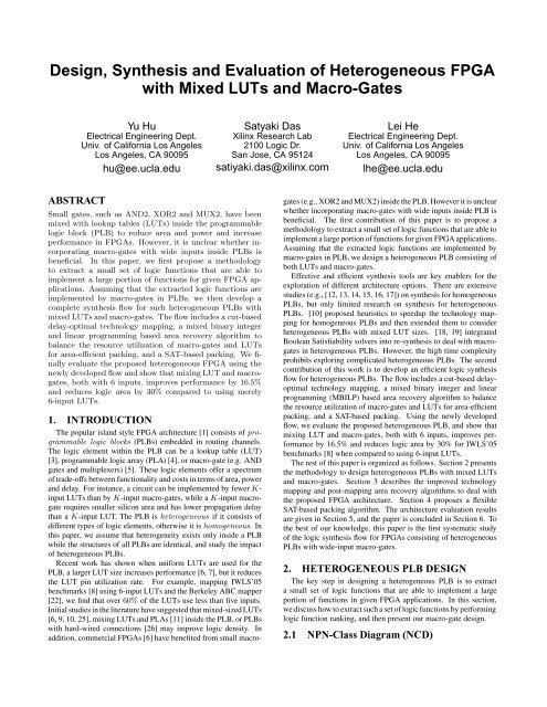
elated to the other input pins <strong>and</strong> to other possible nets will also begenerated as needed.Certain input pins <strong>of</strong> logic elements are swappable, i.e., they maybe interchanged if it helps <strong>with</strong> producing a valid PLB. Variablesare introduced to encode the choice <strong>of</strong> equivalent pins that havebeen swapped <strong>and</strong> equivalent pin constraints corresponding tothese added.Finally, boundary constraints forcing input (or output) nets tobe assigned to at least one <strong>of</strong> the input (or output) pins are added.An example <strong>of</strong> such a constraint is(a)(b)Figure 9: (a) Architecture <strong>of</strong> a <strong>FPGA</strong> PLB, (b) Subcircuitto be packedplaced at at least one <strong>of</strong> the sites A <strong>and</strong> B. The two equations aboveguarantee that X would be placed at exactly one location. Similarconstraints would be generated for the flip flop Z <strong>and</strong> the possiblelocations D <strong>and</strong> E.Nets are treated like logic element sites, which are encoded asBoolean variables, U i@N j (∀i ∈ {1 · · · 8}, j ∈ {0 · · · 15}). Themutual exclusion conditions apply on nets, as well, so that distinctnets in the user netlist cannot be present at any one net in the PLB.We also have input <strong>and</strong> output constraints for all logic elements.One such output constraint would beX@A → U 5@N 10, (37)which guarantees that if X is placed at location A in the PLB, thenthe N 10 net in the PLB carries the U 5 signal. Input constraints shallalso be generated in an analogous fashion.For routing multiplexers (like G <strong>and</strong> H) which are controlled byconfiguration logic we have variables that determine which inputdrives the output. So for G, we would have the variables, G 0→out<strong>and</strong> G 1→out, <strong>and</strong> we need to add exclusive driver constraints(38) so that no output is driven by two inputs. We also need to addrouting constraints (39) so that if a net is present at an input toa routing multiplexer <strong>and</strong> the appropriate control bit is active thenthe output has the correct net.G 0→out → (¬G 1→out) (38)(G 0→out ∧ U 5@N 10) → U 5@N 12 (39)Finally, extra variables are needed to encode the choice that somelogic elements can act as route-throughs. An example <strong>of</strong> such anelement is a lookup table. It can be programmed to pass one <strong>of</strong>its inputs out to the output <strong>and</strong> thus act like a routing multiplexerif it is not being used. This increases the routing flexibility if weneed it. Corresponding to these extra variables, route-throughconstraints are generated. For example, some <strong>of</strong> the constraintsgenerated for taking into consideration that LUT B might be usedas a route-through are(RT B ∧ B 0→out) → (¬B 1→out) (40)(RT B ∧ B 0→out ∧ U8@N5) → U8@N11 (41)where RT B encodes the choice as to whether LUT B is used as aroute-through. Constraint (40) maintains that inputs 0 <strong>and</strong> 1 cannotdrive the output simultaneously. There will be other constraints correspondingto mutual exclusion <strong>of</strong> every pair <strong>of</strong> inputs. Constraint(41) specifies that if input 0 does drive the output <strong>and</strong> if net N 5 isat input 0, then it would also appear at the output. Note that constraint(40) is just a representative constraint <strong>and</strong> other constraintsU 6@N 13 ∨ U 6@N 14 ∨ U 6@N 15 (42)Once all the constraints are automatically generated from a topologicaldescription <strong>of</strong> the PLB graph <strong>and</strong> the logic elements in theuser’s netlist that we wish to pack into a PLB, we use a SAT-solver tocheck if they can all be satisfied simultaneously. If they are all satisfied,we can generate a valid placement <strong>and</strong> route from the solutionthat the SAT solver gives us. Translating the solution to an assignment<strong>of</strong> netlist elements to PLB locations, PLB input pins to nets<strong>and</strong> control bits in the routing multiplexers is easy. We construct thePLB based on all the variables that are TRUE in the satisfying assignment.In our example, the satisfying assignment could have thefollowing variables be TRUE U 1@N 0, U 2@N 1, · · · , X@A, RT B,where U 1@N 0 means that the net U 1 is at the PLB input N 0, X@Ameans that LUT X is placed at location A <strong>and</strong> RT B means thatLUT B is used as a route-through.The principal advantage <strong>of</strong> this method is that we can validatePLB packing for different PLB architectures <strong>with</strong>out any architecturespecific code. This method can be especially useful for newarchitectures before specialized code has been written to validatepacking <strong>and</strong> also to check correctness <strong>of</strong> the specialized code duringregression testing. The method is also applicable for architectureexploration as it is infeasible to write specialized valid packingcheckers for all c<strong>and</strong>idate architectures.5. ARCHITECTURE EVALUATION5.1 Area <strong>and</strong> Delay ModelingSuggested in [4], an LUT-4 can be implemented by 16 1-bitSRAM, 4 inverters <strong>and</strong> 15 2:1MUXes which are 16 × 6 + 4 × 2 +15 × 4 = 164 transistors 6 . Following the <strong>FPGA</strong> area modeling in[4], an LUT-6 can be implemented by 64 1-bit SRM, 6 inverters <strong>and</strong>63 2:1MUXes <strong>and</strong> a macro-gate in Figure 4 can be implementedby 9 1-bit SRM, 7 inverters, 3 2:1MUXes <strong>and</strong> 63 transistors (forimplementing the embedded logic gates g 1, · · · , g 4). Hence thenumber <strong>of</strong> transistors needed to implement a macro-gate <strong>and</strong> anLUT-6 is 143 <strong>and</strong> 648, respectively. Due to the space limit we omitthe schematics <strong>of</strong> the implementation. The logic delay is modeledby the square root <strong>of</strong> the logic area. The area <strong>and</strong> delay modelsused in our experiments are summarized in Table 2.LUT-4 macro-gate LUT-6transistor number 164 143 648normalized area 1.15 1.00 4.53normalized delay 1.07 1.00 2.13Table 2: Summary <strong>of</strong> the area <strong>and</strong> delay models5.2 Experimental ResultsWe implement the improved mapping algorithms in BerkeleyABC platform [22] <strong>with</strong> C language <strong>and</strong> the SAT-based packer <strong>with</strong>6 [4] assumes that a 1-bit SRAM, an inverter <strong>and</strong> a 2:1MUX needs 6,2 <strong>and</strong> 4 transistors, respectively.
circuit Logic depth Estimated delay (normalized) PLB# Estimated area (normalized)LUT4 LUT4 LUT6 LUT6 LUT4 LUT4 LUT6 LUT6 LUT4 LUT4 LUT6 LUT6 LUT4 LUT4 LUT6 LUT6MG MG MG MG MG MG MG MGac97 ctrl 4 4 3 4 4 4 6 4 4010 1739 2898 1523 4599 3733 13132 8424aes core 8 7 6 9 8 7 12 10 8959 4147 3912 2932 10275 8903 17727 16218des area 10 10 7 10 10 10 14 11 2153 1004 968 674 2469 2154 4386 3728des perf 6 6 4 7 6 6 8 7 32371 15652 6872 4863 37125 33601 31140 26900ethernet 10 9 7 9 10 9 14 12 5047 2438 3953 2215 5788 5234 17913 12252i2c 5 4 4 4 5 4 8 6 392 188 265 144 450 404 1201 794mem ctrl 11 9 8 9 11 9 16 12 3687 1731 2892 1413 4228 3715 13105 7813pci bridge32 9 8 7 8 9 8 14 11 6596 3156 5413 2911 7565 6774 24529 16102pci spoci ctrl 6 5 5 5 6 5 10 7 372 173 251 137 427 370 1137 755sasc 3 3 2 4 3 3 4 4 206 87 147 85 236 186 666 470simple spi 4 4 3 4 4 4 6 4 295 121 200 113 338 259 906 625spi 10 9 7 9 10 9 14 11 1315 601 913 440 1508 1289 4137 2431ss pcm 3 3 2 3 3 3 4 3 124 61 102 48 142 131 462 266systemcaes 11 11 8 13 11 11 16 16 2948 1470 1926 1158 3381 3155 8728 6405systemcdes 9 8 5 9 9 8 10 10 1125 580 608 351 1290 1245 2755 1942tv80 17 15 11 15 17 15 22 20 2963 1404 2132 1129 3398 3013 9661 6245usb funct 9 9 6 9 9 9 12 10 4906 2227 3408 1775 5626 4781 15443 9816usb phy 4 3 2 3 4 3 4 4 188 89 145 60 216 190 657 332vga lcd 7 7 6 7 7 7 12 9 40814 18145 28791 16561 46808 38954 130466 91604wb conmax 9 7 6 7 9 7 12 10 14580 6966 11003 5895 16721 14954 49860 32608wb dma 10 9 6 9 10 9 12 11 1469 711 1129 579 1685 1525 5116 3200average 7.86 7.14 5.48 7.48 7.86 7.14 10.95 9.14 6406 2985 3711 2142 7346 6408 16816 11849Table 1: Delay <strong>and</strong> area comparisons among different architecturesLISP language, <strong>and</strong> test them on IWLS’05 benchmarks [8]. TheMBILP <strong>and</strong> SAT problem are solved by mosek [24] <strong>and</strong> zChaff[23], respectively.Table 1 compares four architectures, i.e., a PLB containing anLUT-4 (column “LUT4”), the mix <strong>of</strong> an LUT-4 <strong>and</strong> a macro-gatein Figure 4 (column “LUT4+MG”), an LUT-6 (column “LUT6”),<strong>and</strong> the mix <strong>of</strong> an LUT-6 <strong>and</strong> a macro-gate (column “LUT6+MG”),respectively. The logic depth, number <strong>of</strong> PLBs, estimated delay<strong>and</strong> area 7 <strong>of</strong> the circuits <strong>with</strong> different architectures are shown inthe table. Compared to LUT-4 only architecture, the mix <strong>of</strong> LUT-4 <strong>and</strong> macro-gates reduces both logic depth <strong>and</strong> logic delay by9.2%, <strong>and</strong> reduces logic area by 12.9%. Compared to LUT-6 onlyarchitecture, the mix <strong>of</strong> LUT-6 <strong>and</strong> macro-gates reduces logic delay<strong>and</strong> logic area by 16.5% <strong>and</strong> 30%, respectively, while it increasesthe logic depth by 36.5%. The average logic depth <strong>of</strong> mixing LUT-6<strong>and</strong> macro-gate is larger than that for mixing LUT-4 macro-gatesbecause our technology mapper sets the delay weight <strong>of</strong> an LUT-6<strong>and</strong> a macro-gate as 2.13:1.00 based on Table 2.In addition, the experimental results show that the functionalpruning (FP) technique (Subsection 3.1) used in technology mappingprunes 30% more cuts <strong>and</strong> reduces 8% overall runtime comparedto the algorithm <strong>with</strong>out using FP. More improvement isexpected when larger macro-gates are used. Furthermore, the logicarea is reduced by 5% due to the MBILP based area recovery algorithm(Subsection 3.2).6. CONCLUSIONS AND FUTURE WORKTargeting macro-gate based heterogeneous <strong>FPGA</strong>s, a methodologyhas been proposed to extract a small set <strong>of</strong> logic functions thatare able to implement a large portion <strong>of</strong> functions for given <strong>FPGA</strong>applications. Assuming that the extracted logic functions are implementedby macro-gates in PLBs, a complete synthesis flow hasbeen developed for such heterogeneous PLBs <strong>with</strong> mixed LUTs <strong>and</strong>macro-gates. The flow includes a cut-based delay-optimal technologymapping, a mixed binary integer <strong>and</strong> linear programming basedarea recovery algorithm to balance the resource utilization <strong>of</strong> macrogates<strong>and</strong> LUTs for area-efficient packing, <strong>and</strong> a SAT-based packing.The proposed heterogeneous <strong>FPGA</strong> design has been evaluated usingthe newly developed flow. The experimental results show thatmixing LUT <strong>and</strong> macro-gates, both <strong>with</strong> 6 inputs, improves perfor-7 Given areas in Table 2, the area ratio between these four PLBs is1.15:(1.15+1):4.53:(4.53+1).mance by 16.5% <strong>and</strong> reduces logic area by 30% compared to using6-input LUTs.In the future, we will investigate more complicated macro-gatebased heterogeneous PLBs architectures by the proposed synthesisflow, <strong>and</strong> consider area, delay <strong>and</strong> power optimization during thetechnology mapping <strong>and</strong> packing processes. We will also connectour synthesis flow <strong>with</strong> the back-end tools such as placement <strong>and</strong>routing for even more accurate architecture evaluation consideringboth logic <strong>and</strong> routing cost.7. REFERENCES[1] V. Betz, J. Rose, <strong>and</strong> A. Marquardt, Architecture <strong>and</strong> CAD for Deep-Submicron<strong>FPGA</strong>s. Kluwer Academic Publishers, 1999.[2] P. Jamieson <strong>and</strong> J. Rose, “A verilog RTL synthesis tool for heterogeneous<strong>FPGA</strong>s,” in <strong>FPGA</strong>, 2005.[3] “The programmable gate array data book,” in Xilinx, 1989.[4] J. Cong, H. Huang, <strong>and</strong> X. Yuan, “Technology mapping <strong>and</strong> architectureevaluation for k/m-macrocell-based <strong>FPGA</strong>s,” ACM TODAES, 2005.[5] “Xilinx product datasheets,” in http://www.xilinx.com/literature.[6] A. Cosoroaba <strong>and</strong> F. Rivoallon, “Achieving higher system performance<strong>with</strong> the virtex-5 family <strong>of</strong> <strong>FPGA</strong>s,” in http://www.xilinx.com/literature.[7] F. Li <strong>and</strong> L. He, “Power modeling <strong>and</strong> characteristics <strong>of</strong> fieldprogrammable gate arrays,” IEEE TCAD, 2005.[8] “Iwls 2005 benchmarks,” in http://iwls.org/iwls2005/benchmarks.html.[9] J. Cong <strong>and</strong> S. Xu, “Delay-optimal technology mapping for <strong>FPGA</strong>s <strong>with</strong>heterogeneous LUTs,” in DAC, 1998.[10] J. Cong, C. Wu, <strong>and</strong> Y. Ding, “Cut ranking <strong>and</strong> pruning: Enabling ageneral <strong>and</strong> efficient fpga mapping solution,” in <strong>FPGA</strong>, 1999.[11] A. Kaviani <strong>and</strong> S. Brown, “Hybrid <strong>FPGA</strong> architecture,” in <strong>FPGA</strong>, 1996.[12] J. Cong <strong>and</strong> Y. Ding, “Flowmap: An optimal technology mappingalgorithm for delay optimization in lookup-table based <strong>FPGA</strong> designs,” inIEEE TCAD, 1994.[13] J. Cong <strong>and</strong> Y. Ding, “On area/depth trade-<strong>of</strong>f in LUT-based <strong>FPGA</strong>technology mapping,” in IEEE TVLSI, 1994.[14] D. Chen <strong>and</strong> J. Cong, “Daomap: A depth-optimal area optimizationmapping algorithm for <strong>FPGA</strong> designs,” in ICCAD, 2004.[15] V. Manohara-rajah, S. D. Brown, <strong>and</strong> Z. G. Vranesic, “Heuristics for areaminimization in LUT-based <strong>FPGA</strong> technology mapping,” in IWLS, 2004.[16] A. Mishchenko, S. Chatterjee, R. Brayton, <strong>and</strong> P. Pan, “Integrating logicsynthesis, technology mapping, <strong>and</strong> retiming,” in IWSL, 2005.[17] S. Chatterjee, A. Mishchenko, <strong>and</strong> R. Brayton, “Factor cuts,” in ICCAD,2006.[18] A. Ling, D. Singh, <strong>and</strong> S. Brown, “Fpga logic synthesis using quantifiedboolean satisfiability,” in SAT 2005 Springer LNCS Vol 3569, pp. 444–450.[19] S. Safarpour, A. Veneris, G. Baeckler, <strong>and</strong> R. Yuan, “Efficient SATbasedboolean matching for fpga technology mapping,” in DAC[20] D. Chai <strong>and</strong> A. Kuehlmann, “Building a better boolean matcher <strong>and</strong>symmetry detector,” in DATE, 2006.[21] S. C. Soheil Ghiasi, Elaheh Bozorgzadeh <strong>and</strong> M. Sarrafzadeh, “A unifiedtheory <strong>of</strong> timing budget management,” in ICCAD, 2004.[22] “Abc: A system for sequential synthesis <strong>and</strong> verification,” inhttp://www.eecs.berkeley.edu/ alanmi/abc/.[23] M. Moskewicz, C. Madigan, Y. Zhao, L. Zhang, <strong>and</strong> S. Malik,“Chaff:Engineering an endcient SAT solver,” in DAC, 2001.[24] http://www.mosek.com.[25] Jianshe He, “Technology Mapping <strong>and</strong> Architecture <strong>of</strong> HeterogenousField-Programmable Gate Arrays,” M.A.Sc. Thesis, University <strong>of</strong> Toronto,1993.[26] Kevin Chung, “Architecture <strong>and</strong> <strong>Synthesis</strong> <strong>of</strong> Field-Programmable GateArrays <strong>with</strong> Hard-wired Connections,” Ph.D. Thesis, University <strong>of</strong>Toronto, 1994.