Lecture 4: Karnaugh Maps, Timing Diagrams ... - CS-CSIF
Lecture 4: Karnaugh Maps, Timing Diagrams ... - CS-CSIF
Lecture 4: Karnaugh Maps, Timing Diagrams ... - CS-CSIF

You also want an ePaper? Increase the reach of your titles
YUMPU automatically turns print PDFs into web optimized ePapers that Google loves.
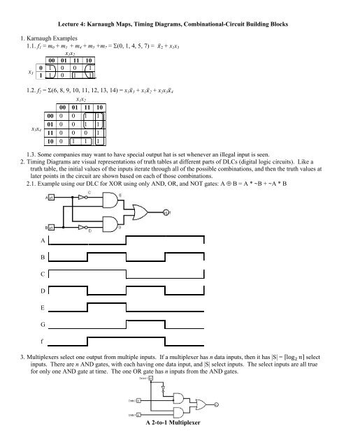
<strong>Lecture</strong> 4: <strong>Karnaugh</strong> <strong>Maps</strong>, <strong>Timing</strong> <strong>Diagrams</strong>, Combinational-Circuit Building Blocks1. <strong>Karnaugh</strong> Examples1.1. f 1 = m 0 + m 1 + m 4 + m 5 +m 7 = Σ(0, 1, 4, 5, 7) = x̅2 + x 1 x 3x 1 x 200 01 11 10x 30 1 0 0 11 1 0 1 11.2. f 2 = Σ(6, 8, 9, 10, 11, 12, 13, 14) = x 1 x̅3 + x 1 x̅2 + x 2 x 3 x̅4x 1 x 200 01 11 1001 0 0 1 1x 3 x 411 0 0 0 100 0 0 1 110 0 1 1 11.3. Some companies may want to have special output hat is set whenever an illegal input is seen.2. <strong>Timing</strong> <strong>Diagrams</strong> are visual representations of truth tables at different parts of DLCs (digital logic circuits). Like atruth table, the initial values of the inputs iterate through all of the possible combinations, and then the truth values atlater points in the circuit are shown based on each of those combinations.2.1. Example using our DLC for XOR using only AND, OR, and NOT gates: A ⊕ B = A * ~B + ~A * BABCDEGf3. Multiplexers select one output from multiple inputs. If a multiplexer has n data inputs, then it has |S| = ⌈log 2 n⌉ selectinputs. There are n AND gates, with each having one data input, and |S| select inputs. The select inputs are all truefor only one AND gate at time. The one OR gate has n inputs from the AND gates.A 2-to-1 Multiplexer
3.1. Multiplexers are used to control signal and data routing.3.2. We can use a n-input MUX to implement any Boolean equation of log 2 (n) variables by feeding the variables to theselect inputs, and setting the data inputs to the expected values for the equation.3.2.1. For the following 4-to1 MUX, what are the constant voltages (high = true, low = false) applied to the four Datainputs to implement XOR based the select inputs?4. Decoders s are combinational circuits that convert binary information from n input lines to a maximum of 2 n uniqueoutput lines.4.1. For many designs, only one output is asserted at a time, which is called one-hot encoded. This type is extremelyimportant in memory circuits, since you give an address that is encoded and one of the spots in the memory hasto be selected. Most kinds of random-access memory use a n-to-2 n decoder to convert the selected address on theaddress bus to one of the row address select lines.4.2. An additional input that is attached to all of the AND gates can be used in two ways.4.2.1. If data is fed to that input, then the decoder can be used a s demultiplexer that guides the data to a specificoutput, i.e. a 2 n -to-1 demultiplexer.4.2.2. If the additional input line is thought of as a separate enabling input, then it is a way to turn the decoder on oroff.5. Adder = a digital circuit that adds two numbers.5.1. Half adder adds two single binary digits A and B. It has two outputs, sum (S) and carry (C).5.2. Full adder adds binary numbers and accounts for values carried in as well as out. Notice that the longest path (A to C out )goes through three gates. This will be involved in determining the clock speed.
5.3. Two types of multiple-bit adders.5.3.1. Ripple-carry adder = an adder in which each full adder uses C out of the previous bit as its C in . This causes adelay as the signal propagates through the gates of each full adder.5.3.2. Carry-lookahead adder = They work by creating two signals (p and g) for each bit position, based on if a carry ispropagated through from a less significant bit position (at least one input is a '1'), a carry is generated in that bitposition (both inputs are '1'), or if a carry is killed in that bit position (both inputs are '0'). In most cases, p issimply the sum output of a half-adder and g is the carry output of the same adder. After p and g are generated thecarries for every bit position are created. (Wikipedia) This permits the adders to work simultaneously.5.3.3. c i+1 = g i + p i c i , where g i = x i y i , and p i = x i ⊕ y i .5.3.3.1. Thus c i+1 = g i + pg i-1 + p i p i-1 g i-2 +…+ p i p i-1 …p 2 p 1 g 0 + p i p i-1 …p 1 p 0 c 0 . This expression represents a two-levelAND-OR circuit in which c i+1 is evaluated very quickly.
This is also a great place to motivate/explain why we are "stuck" with two's compliment numbers. Show how we can usethis same adder design to perform subtraction, with only the addition of a mux and an inverter on the outside, andintelligent use of the carry in signal (A-B = A + (-B), and -B = invert B and add one, which is where the carry comes in).