Static Noise Margin Analysis of Various SRAM Topologies - IJET
Static Noise Margin Analysis of Various SRAM Topologies - IJET
Static Noise Margin Analysis of Various SRAM Topologies - IJET
You also want an ePaper? Increase the reach of your titles
YUMPU automatically turns print PDFs into web optimized ePapers that Google loves.
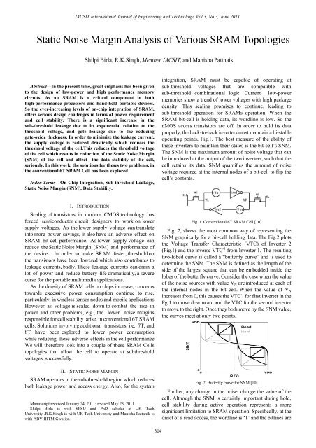
IACSIT International Journal <strong>of</strong> Engineering and Technology, Vol.3, No.3, June 2011<strong>Static</strong> <strong>Noise</strong> <strong>Margin</strong> <strong>Analysis</strong> <strong>of</strong> <strong>Various</strong> <strong>SRAM</strong> <strong>Topologies</strong>Shilpi Birla, R.K.Singh, Member IACSIT, and Manisha PattnaikAbstract—In the present time, great emphasis has been givento the design <strong>of</strong> low-power and high performance memorycircuits. As an <strong>SRAM</strong> is a critical component in bothhigh-performance processors and hand-held portable devices.So the ever-increasing levels <strong>of</strong> on-chip integration <strong>of</strong> <strong>SRAM</strong>,<strong>of</strong>fers serious design challenges in terms <strong>of</strong> power requirementand cell stability. There is a significant increase in thesub-threshold leakage due to its exponential relation to thethreshold voltage, and gate leakage due to the reducinggate-oxide thickness. In order to minimize the leakage current,the supply voltage is reduced drastically which reduces thethreshold voltage <strong>of</strong> the cell.This reduces the threshold voltage<strong>of</strong> the cell which results in reduction <strong>of</strong> the <strong>Static</strong> <strong>Noise</strong> <strong>Margin</strong>(SNM) <strong>of</strong> the cell and affect the data stability <strong>of</strong> the cell,seriously. In this work, the solutions for theses two problems, inthe conventional 6T <strong>SRAM</strong> Cell has been explored.Index Terms—On-Chip Integration, Sub-threshold Leakage,<strong>Static</strong> <strong>Noise</strong> <strong>Margin</strong> (SNM), Data Stability.integration, <strong>SRAM</strong> must be capable <strong>of</strong> operating atsub-threshold voltages that are compatible withsub-threshold combinational logic. Current low-powermemories show a trend <strong>of</strong> lower voltages with high packagedensity. This scaling promises to continue, leading tosub-threshold operation for <strong>SRAM</strong>s operation. When the<strong>SRAM</strong> bit-cell is holding data, its wordline is low. So thenMOS access transistors are <strong>of</strong>f. In order to hold its dataproperly, the back-to-back inverters must maintain a bi-stableoperating points, Fig.1. The best measure <strong>of</strong> the ability <strong>of</strong>these inverters to maintain their states is the bit-cell’s SNM.The SNM is the maximum amount <strong>of</strong> noise voltage that canbe introduced at the output <strong>of</strong> the two inverters, such that thecell retains its data. SNM quantifies the amount <strong>of</strong> noisevoltage required at the internal nodes <strong>of</strong> a bit-cell to flip thecell’s contents.I. INTRODUCTIONScaling <strong>of</strong> transistors in modern CMOS technology hasforced semiconductor circuit designers to work on lowersupply voltages. As the lower supply voltage can translateinto more power savings, it also have an adverse effect on<strong>SRAM</strong> bit-cell performance. As lower supply voltage canreduce the <strong>Static</strong> <strong>Noise</strong> <strong>Margin</strong> (SNM) and performance <strong>of</strong>the device. In order to make <strong>SRAM</strong> faster, threshold onthe transistors have been lowered which also contributes toleakage currents, badly. These leakage currents can drain alot <strong>of</strong> power and reduce battery life dramatically, a severecurse for the portable multimedia applications.As the density <strong>of</strong> <strong>SRAM</strong> cells on chips increase, concernstowards excessive power consumption continue to rise,particularly, in wireless sensor nodes and mobile applications.However, as voltage is scaled down to combat the rise inpower and other problems, e.g., the lower noise marginsresponsible for cell stability arise in conventional 6T <strong>SRAM</strong>cells. Solutions involving additional transistors, i.e., 7T, and8T have been explored to lower power consumptionwhile reducing these adverse effects in the cell performance.We will therefore look into a couple <strong>of</strong> these <strong>SRAM</strong> Cellstopologies that allow the cell to operate at subthresholdvoltages, successfully.Fig. 1. Conventional 6T <strong>SRAM</strong> Cell [10]Fig. 2, shows the most common way <strong>of</strong> representing theSNM graphically for a bit-cell holding data. The Fig.2 plotsthe Voltage Transfer Characteristic (VTC) <strong>of</strong> Inverter 2(Fig.1) and the inverse VTC -1 from Inverter 1. The resultingtwo-lobed curve is called a “butterfly curve” and is used todetermine the SNM. The SNM is defined as the length <strong>of</strong> theside <strong>of</strong> the largest square that can be embedded inside thelobes <strong>of</strong> the butterfly curve. Consider the case when the value<strong>of</strong> the noise sources with value V N are introduced at each <strong>of</strong>the internal nodes in the bit cell. When the value <strong>of</strong> V Nincreases from 0, this causes the VTC -1 for first inverter in theFg.1 to move downward and the VTC for the second inverterto move to the right. Once they both move by the SNM value,the curves meet at only two points.II. STATIC NOISE MARGIN<strong>SRAM</strong> operates in the sub-threshold region which reducesboth leakage power and access energy. Also, for the systemManuscript received January 24, 2011; revised May 23, 2011.Shilpi Birla is with SPSU and PhD scholar at UK TechUniversity .R.K.Singh is with UK Tech University and Manisha Pattanik iswith ABV-IIITM Gwalior.Fig. 2. Butterfly curve for SNM [10]Further, any change in the noise, change the value <strong>of</strong> thecell. Although the SNM is certainly important during hold,cell stability during active operation represents a moresignificant limitation to <strong>SRAM</strong> operation. Specifically, at theonset <strong>of</strong> a read access, the wordline is ‘1’ and the bitlines are304
IACSIT International Journal <strong>of</strong> Engineering and Technology, Vol.3, No.3, June 2011still precharged to ‘1’. The internal node <strong>of</strong> the bit-cell thatrepresents a zero gets pulled upward through the accesstransistor due to the voltage dividing effect across the accesstransistor and drive transistor. This increase in voltageseverely degrades the SNM during the read operation (readSNM) as shown in the Fig.3. The butterfly curve during holdand read illustrates the degradation in SNM during read.C. Dependence <strong>of</strong> SNM on Sizing <strong>of</strong> the TransistorsThe cell ratio has very little impact on SNM duringsub-threshold read. The lower impact <strong>of</strong> sizing is reasonableconsidering the exponential dependence <strong>of</strong> sub-thresholdcurrent on other parameters. Fig. 6 shows that the sizingchange affects linearly and only have a logarithmic impact onthe VTCs. As a result <strong>of</strong> narrow or short channel effects, theV T for deep submicron devices tends to vary with size. Theseeffects depend on the technology and make the general SNMmodeling more complicated, see [10,21].Fig. 3. Butterfly Curves during Read and Write [10]III. SNM DEPENDENCIESThis section explores the different parameters on which theSNM is dependent. The factors are supply voltage,temperature and doping variations.A. Dependence <strong>of</strong> SNM on VddThe SNM for a bit-cell with ideal VTCs is still limitedV dd /2 to because <strong>of</strong> the two sides <strong>of</strong> the butterfly curve. Anupper limit on the change in SNM with V dd is thus 1/2. Fig. 4,plots SNM versus V dd directly for both, hold and read mode.From [10], the slopes <strong>of</strong> the curves confirm that less than 1/2V dd <strong>of</strong> noise will translate into SNM changes.Fig. 4. SNM versus Vdd Curve [10]B. Dependence <strong>of</strong> SNM on TemperatureFig.5. SNM versus Temperature Curve [21][21] it is shown that the exponential dependence <strong>of</strong> currenton sub-threshold operation increases the random variationeffects.Fig. 6. SNM versus Cell Ratio Curve [10]IV. READ AND WRITE ABILITY OF <strong>SRAM</strong> CELLSThere are three operating modes in <strong>SRAM</strong>, standby, read,and write. Each mode can define its own operating margin.When the cell is in the standby, its wordline (WL) isconnected to the ground. In order to hold its data properly,the cross-coupled two inverters in the cell must sustainbi-stable operating points. As shown in [14], the SNM is acommon measure <strong>of</strong> the ability for the cell inverters tomaintain their state. The SNM equals the minimum noisevoltage present at each <strong>of</strong> the data storage nodes (VL, VR)necessary to flip state <strong>of</strong> the cell. As shown in the dotted linein Fig.2, it is graphically defined as the length <strong>of</strong> side <strong>of</strong> thepossible maximum square between the normal and inversevoltage transfer characteristic (VTC) <strong>of</strong> two identical cellinverters. Specifically, the Conventional 6T <strong>SRAM</strong> cell ismore sensitive to noise during read access. When the cell is in,the read access, the wordline is connected to V dd while thebit-line pairs (BL, BLB) are precharged to V dd . The data ‘0’storage node rises to a certain voltage higher than the groundaccording to the voltage dividing across the access transistorand driver transistor. Moreover, the gain <strong>of</strong> the <strong>Static</strong>Transfer Characteristic (STC) is lowered due to the parallelconnection <strong>of</strong> the conducting access transistor and the loadPMOS transistor. This severely degrades the cell immunity tonoise. The side <strong>of</strong> the possible maximum square nestedbetween the normal and inverse VTC during the read accessthus equals the read SNM <strong>of</strong> the cell. It is represented by thesolid line in Fig. 3.In the Fig. 7 (a), a conceptual setup measuring for the cellwrite margin is shown. Let’s assume that the inv-1 side in thecell initially holds a data ‘0’ and the inv-2 side holds a data‘1’, respectively. When the cell is in the write access, theword-line is connected to V dd , while the bitline pairs aredriven to V dd and the ground to flip the cell state. Then, thedata storage node <strong>of</strong> inverter-2 side will be falling down from305
IACSIT International Journal <strong>of</strong> Engineering and Technology, Vol.3, No.3, June 2011V . dd The figure plots the respective transfer characteristics <strong>of</strong>the cell inverters in this write access. Particularly, whenobtaining the characteristic <strong>of</strong> inverter-2 side, the wordlinevoltage <strong>of</strong> its access transistor is used as an input signal,,while the input node <strong>of</strong> inverter-2 is set to V OL the lowestvoltage level <strong>of</strong> the output <strong>of</strong> inverter-1. Since the output <strong>of</strong>inverter-1, V DN , will not be reversed until the output <strong>of</strong>inverter-2, V /DN , reaches a logic threshold voltage (V LT ) <strong>of</strong>inverter-1, the margin 0V is assumed to occur when V /DNequals V LT <strong>of</strong> inverter-1. Here, the voltage level <strong>of</strong> WL forthe case <strong>of</strong> margin 0V is referred to as VWL0. This is atrigger for the cell to begin a toggle.,Because the voltage level <strong>of</strong> accessed WL is V dd thewrite margin (WM) is thus defined as V dd –VWL0. This writemargin quantifies a surplus amount between the accessed WLvoltage and the minimum WL voltage required for the cell t<strong>of</strong>lip its contents.increases, the write margin improves. The write margin inthis case is 0.6V. This voltage is above V , T so, the PMOS hasweakened relative to the NMOS because the mobility.dominates the differences in V T Even at 0.6V, the writemargin is barely negative for the worst-case corner and thisdoes not account for local V T variations. For these reasons,V dd at 0.6V is the best case voltage for which we can expecttraditional write operations to work for a sub-thresholdmemory in this 65-nm process [8].A. 7T <strong>SRAM</strong> CellA read SNM free <strong>SRAM</strong> is implemented in [8]. But thelimitation was the write operations at the lower V dd cannot beperformed and the read operations at low V dd levels result inlow storage destructions in <strong>SRAM</strong> cells due to the leakagecurrent <strong>of</strong> PMOS cells. The other 7T <strong>SRAM</strong> cell (Fig. 8) usesa novel write mechanism which depends only on one <strong>of</strong> the2-bit lines to perform a write operation, which reduces theactivity factor <strong>of</strong> discharging the bit-line pair. Simulationshows that the write power saving is at least 49% [8,9]. Both,the read delay and the static noise margins are maintainedafter carefully sizing the cell transistors. The limitation isarea overhead from conventional 6T <strong>SRAM</strong> cell [9].Fig. 8 7T <strong>SRAM</strong> Cell with Novel Write Mechanism [9]B. 8T <strong>SRAM</strong> CellA dual-port 8T-<strong>SRAM</strong> cell is created by adding two dataoutput transistors to a conventional 6T-<strong>SRAM</strong> cell (Fig. 9).Separation <strong>of</strong> data retention element and data output elementmeans there will be no correlation between read SNM andI cell .(a)(b)Fig. 7. Operating <strong>Margin</strong> <strong>of</strong> 6T <strong>SRAM</strong> Cell(a) SNM during Standby and Read and (b) Write <strong>Margin</strong> [14]V. <strong>SRAM</strong> TOPOLOGIES<strong>Various</strong> <strong>SRAM</strong> topologies have been analyzed in thissection and implemented at various process technologies.<strong>Various</strong> types <strong>of</strong> <strong>SRAM</strong>s are implemented and the stabilityfactor (SNM) has been analyzed for them.The conventional 6T <strong>SRAM</strong> Cell is implemented at 65nmnode and the analysis <strong>of</strong> the stability is done. A 6T <strong>SRAM</strong> isdesigned in the 65-nm process. In this the iso-size PMOSdevices are stronger in sub-V T than NMOS by roughly anorder <strong>of</strong> magnitude, which makes the write functionalitymore challenging. The general trend showing animprovement <strong>of</strong> write operation, i.e., more negative margin,at higher temperature occurs because the PMOS transistorsweaken relative to NMOS as temperature rises. As V ddFig. 9 Dual-Port 8T <strong>SRAM</strong> Cell [14]In contrast to the worst normalized read SNM value <strong>of</strong>0.20 for a conventional 6T-<strong>SRAM</strong> cell, here the value is 1.22,and there is no I cell degradation. It is also possible here, tolower the Vth <strong>of</strong> the NMOS transistors in a <strong>SRAM</strong> cell inorder to improve I cell . As shown in [9], this 8T-<strong>SRAM</strong> cellhas 30% more area than a conventional 6T-<strong>SRAM</strong> cell,however. The 30% area overhead is composed <strong>of</strong> not only thetwo added transistors but also <strong>of</strong> the contact area <strong>of</strong> the WWL,the word-line for write operations. While WL contact area isconventionally assigned to the boundary line between two<strong>SRAM</strong> cells, in this <strong>SRAM</strong> cell the WWL contact area isassigned to within a cell, as shown in Fig. 9.An UDVS (Ultra Dynamic Voltage Scaling) 8T-<strong>SRAM</strong>(Fig. 10) is proposed in this read and write ports aredecoupled, (BVSS) virtual ground node for read buffer and iskept at V dd is cell is not accessed. Mchd is the virtual supplynode and its voltage can be brought down during write accessupto weaken PMOS. A 64Kb <strong>SRAM</strong> fabricated with a die306
IACSIT International Journal <strong>of</strong> Engineering and Technology, Vol.3, No.3, June 2011size <strong>of</strong> 1.4mmX1mm. At 250mv supply voltage, 20 KHzfrequency is obtained and at 1.2V, 200 MHz frequency isobtained. Low voltage operation is successfully achieved.The RSNM (Read <strong>Static</strong> <strong>Noise</strong> <strong>Margin</strong>) problem is alsoresolved. The only limitation is the area overhead asmentioned in [20].and WM (Write <strong>Margin</strong>), also improved. Another type <strong>of</strong>10T <strong>SRAM</strong> cell is as shown in Fig. 11. It shows a schematic<strong>of</strong> a 10T <strong>SRAM</strong> cell with differential read bitlines (RBL and/RBL) . Two NMOS transistors (N5 and N7) for the RBL andthe other additional NMOS transistors (N6 and N8) for /RBLare appended to the conventional 6T <strong>SRAM</strong> cell. As well asthe 8T <strong>SRAM</strong> cell, precharge circuits must be implementedon the RBL and /RBL [2, 6].Fig. 10 U-DVS 8T <strong>SRAM</strong> Cell [18]In [18], other type an 8T <strong>SRAM</strong> cell with variabilitytolerance is proposed. A two Transistor read stack is addedwith conventional 6T <strong>SRAM</strong> cell. Elimination <strong>of</strong> columnselect when the 8T array is floor planned, so that all the bitsare spatially adjacent. From [18] the proposed 32kb sub-arrayoperates at 5.3GHz at 1.2 V and 295MHz at 0.41V. This<strong>SRAM</strong> improves variability tolerance due to processvariation, temperature, and voltage and has SNMImprovement.An 8T sub-threshold <strong>SRAM</strong> with sense amplifier has beenproposed. It has ‘zero’ leakage read buffer. To resolve readbuffer footer limitation charge pump circuit is used. VirtualSupply is used V dd for internal feedback control as proposedin [17]. It uses Sense Amplifier Redundancy concept. Cellstability is also taken care in this and buffered read is used toensure read stability.The conventional dual-port <strong>SRAM</strong> cell comprised <strong>of</strong> eighttransistors (8T <strong>SRAM</strong>) is shown in Fig. 11. The 8T <strong>SRAM</strong>frees a SNM in a read operation because it has a separatedread port. Meanwhile, a precharge circuit must beimplemented on a read bitline (RBL), so that the two NMOStransistors at the read port can sink a bitline charge to theground. Thus, a certain power is dissipated by precharging.In addition to the precharge circuit, we have to prepare abit-line keeper on the RBL which imparts negative influenceon a readout time. To make the matters worse, the delayoverhead becomes larger as a supply voltage (V DD ) decreasesbecause <strong>of</strong> the bit-line keeper as shown in [7].Fig. 11 Dual-Port 8T <strong>SRAM</strong> Cell [7]C. 10T <strong>SRAM</strong> CellDual Port <strong>SRAM</strong> is used and it has only one read or writecan occur per cycle and operate the <strong>SRAM</strong> in subthresholdregion Fig. 12.The 10T <strong>SRAM</strong> cell can remove the problem <strong>of</strong> read SNMby buffering the stored data during a read access. It has 16%less leakage than the conventional 6T <strong>SRAM</strong> cell. Read SNMFig.12 10T <strong>SRAM</strong> Cell [6]D. 11T <strong>SRAM</strong> CellIn Fig.13, the schematic <strong>of</strong> the proposed 11T-<strong>SRAM</strong>bit-cell is shown. Transistors M2, M4, M5, and M6 areidentical to 6T-<strong>SRAM</strong>, but two transistors M1 and M3 aredownsized to the same size as the PMOS transistors. Thebit-line and word-line are distinct from the write word-line.In this case, memory can have distinct read and write ports.During the hold time, RDWL (Read Wordline) and WL arenot selected. Minimum size transistors were used for theadded 5T-circuitry, except the access transistor that has alarger size. The most important part <strong>of</strong> the 11T-<strong>SRAM</strong> cell isa boost capacitor (CB) that connects source <strong>of</strong> M9 to RDWL[13].Fig. 13 11T <strong>SRAM</strong> Cell [13]Supply voltage is kept at more than 0.3V. In this case, boththe cells are running at a satisfactory speed with a properwrite noise margin. The effective area overhead for theproposed circuit is typically between 22% - 28%, but due toemploying minimum size devices and lowering the sizes <strong>of</strong>PMOS devices in 6T-<strong>SRAM</strong> cell and also downsizing theNMOS transistors in 6T-<strong>SRAM</strong> cell, the area overhead maybe reduced. The SNM is significantly increased (more than6x in some cases compared with 6T-<strong>SRAM</strong> cell) and alsosimulations show that the speed <strong>of</strong> the proposed circuit isfour times higher than the 6T-<strong>SRAM</strong> cell architecture.VI. COMPARISON OF VARIOUS <strong>SRAM</strong> CELLSBrief comparisons with the conventional 6T <strong>SRAM</strong> cellhas been made in respect to the operating voltage andfrequency along with the key features and comments aboutthe power consumption and stability, in Table1 at 65nmprocess technology.307
IACSIT International Journal <strong>of</strong> Engineering and Technology, Vol.3, No.3, June 2011TABLE-I COMPARISON OF VARIOUS <strong>SRAM</strong> CELLSType <strong>of</strong> Cell Technology Stability Stability Comments7T <strong>SRAM</strong> Cell 65 SNM ImprovedPower saving, Operate at720mVArea Overhead from 6T <strong>SRAM</strong> Cell7T <strong>SRAM</strong> Cell using dynamicword-line voltage swingtechnique65RSNM improved by9.5%21% less leakage thanconventional 6TData is not stable for sub V t voltages. 4.8%area overhead from conventional 6T8T <strong>SRAM</strong> Cell having SenseAmplifier Redundancy65 Increased read stability Power constrainedCell stability and power should be taken carefor high speed8T <strong>SRAM</strong> Cell withvariability tolerance65SNM improved, writeability and readabilityimprovedLeakage reductionoperates between 1.2 Vto 0.41VDesign complexity increases.Area overhead from 6T Cell8T <strong>SRAM</strong> Cell withvariability tolerance65SNM improved, writeability and readabilityimprovedLeakage reductionoperates between 1.2 Vto 0.41VDesign complexity increases.Area overhead from 6T Cell8T <strong>SRAM</strong> Cell U-DVS 65RSNMimprovedproblemPower saving operatesfrom 250mV - 1.2VArea overhead from 6T Cell8T <strong>SRAM</strong> Cell using dynamicword-line65Read stabilityimprovement by 80%23% less leakage thanconventional 6T CellOperates in sub-threshold region. 19% areaoverhead from conventional 6T Cell9T <strong>SRAM</strong> Cell 65 SNM improved by 2x22.9% less leakage thanconventional 6T CellSuper cut<strong>of</strong>f scheme is used to reduce theleakage10T <strong>SRAM</strong> Cell 65Read SNM improved,WM also improved16% less leakage than6TOperates in sub threshold.Area inefficient11T <strong>SRAM</strong> Cell 65 SNM improved by 6xLess power consumptionas operates between0.2V - 0.35 VArea overhead by 22-28 %.I. CONCLUSIONIn this paper all, the <strong>SRAM</strong> cell topologies which aredesigned for higher SNM whose stability has been discussedand they are discussed at the 65nm process technology. Asthe process variations is now-a-days a prime concern in therealization <strong>of</strong> the performance <strong>of</strong> a cmos circuit. The stabilityis being measured by the static noise margin curve. Stabilityis the prime concern for today’s <strong>SRAM</strong>s as the leakagereduction is also has to be minimized. In this paper variousdependencies <strong>of</strong> <strong>SRAM</strong> has been given and the various<strong>SRAM</strong> cell has been incorporated with different transistorcells. It gives a road map how the various <strong>SRAM</strong> circuits arebeing designed stating the various features with theirlimitations.ACKNOWLEDGMENTThe authors are very grateful for their respectiveorganizations for their support & encouragement.REFERENCES[1] Jinhui Chen Clark, L.T.Tai-Hua Chen, “An Ultra-Low-Power Memorywith a Subthreshold Power Supply Voltage”, Solid-State Circuits,IEEE Journal, vol.41, Oct 2006, Issue: 10, pp- 2344-2353.[2] Sherif A.Tawfik, Volkan Kursun, “Stability Enhancement Techniquesfor Nanoscale <strong>SRAM</strong> circuits, International SOC design Conference,2008,pp 113-116.[3] Khellah, M.Somasekhar, D. Ye, Y. Kim, N. S. Howard, J. Ruhl,G.Sunna, M.Tschanz, J.Borkar, N.Hamzaoglu, F. Pandya, G.Farhang,A.Zhang, K. De, V. “A 256-Kb Dual-VCC <strong>SRAM</strong> Building Block in65-nm CMOS Process With Actively Clamped Sleep Transistor”,Solid-State Circuits, IEEE Journal ,vol. 42 Jan.2007, Issue 1 , pp.233-242.[4] Zhiyu Liu, Volkan Kursun, “ Characterization <strong>of</strong> a novel NineTransistor <strong>SRAM</strong> cell,IEEE Transactions on Very Large ScaleIntegration Systems,vol.46, Issue 4,April 2008.pp-488-492.[5] Hamzaoglu, F.; Zhang, K.; Yih Wang; Ahn, H.J.; Bhattacharya, U.;Zhanping Chen; Yong-Gee Ng; Pavlov, A.; Smits, K.; Bohr, M , “A 3.8GHz 3 Mb <strong>SRAM</strong> Design With Dynamic Stability Enhancement andLeakage Reduction in 45 nm High-k Metal Gate CMOS Technology” ,Solid-State Circuits, IEEE Journal ,vol. 44 , no. 1, 2009, pp.148 – 154.[6] Benton H. Calhoun Anantha P. Chandrakasan “A 256-kb 65-nmSub-threshold <strong>SRAM</strong> Design for Ultra-Low-Voltage Operation”,Solid-State Circuits, IEEE Journal vol. 42, March 2007, Issue 3 ,pp.680-688.308
IACSIT International Journal <strong>of</strong> Engineering and Technology, Vol.3, No.3, June 2011[7] Hiroki Noguchi et al., “Which is the best dual port <strong>SRAM</strong> in 45nmprocess technology? 8T,10T single end and 10T differential” RenesasTechnology corporation,2008.[8] Koichi Takeda et al, “A Read <strong>Static</strong> <strong>Noise</strong> <strong>Margin</strong> Free <strong>SRAM</strong> cell forLow Vdd and High Speed Applications”, Solidvol. 41, Jan.2006, Issue1 , pp.113-121.[9] Aly, R.E. Bayoumi, M.A., “Low-Power Cache Design Using 7T<strong>SRAM</strong> Cell” Circuits and Systems II: Express Briefs, IEEETransactions, vol. 54 April 2007, Issue: 4, pp. 318-322[10] Benton H. Calhoun Anantha P. Chandrakasan “<strong>Static</strong> <strong>Noise</strong> <strong>Margin</strong>Variation for Sub-threshold <strong>SRAM</strong> in 65 nm CMOS”, Solid-StateCircuits, IEEE Journal vol. 41, Jan.2006, Issue 7, pp.1673-1679.[11] Rajshekhar Keerthi, Henry Chen, “Stability and <strong>Static</strong> <strong>Noise</strong> marginanalysis <strong>of</strong> low power <strong>SRAM</strong>”IEEE International Instrumentation &Measurement Technology Conference, Victoria Canada, May2008,pp-1541-1544.[12] Farshad Moradi etal. “65nm Sub threshold 11 T <strong>SRAM</strong> for ultra lowvoltage Application, IEEE xplore, 2008, pp-113-117.[13] Yeonbae Chung, Seung-Ho Song , “Implementation <strong>of</strong> low-voltagestatic RAM with enhanced data stability and circuit speed”,Microelectronics Journal vol. 40, Issue 6, June 2009, pp. 944-951.[14] Peter Geens, Wim Dehaene, “A dual port dual width 90nm <strong>SRAM</strong> withguaranteed data retention at minimal standby supply voltage”, 34thEuropean Solid-State Circuits Conference, 2008. ESSCIRC2008.pp-290-293.[15] Naveen verma, Anantha P. Chandrakasan ,”A reconfigurable 65nm<strong>SRAM</strong> achieving voltage scalability from 0.25 v-1.2V & performancescalability from 20Khz-200Mhz, 34th European Solid-State CircuitsConference, 2008. ESSCIRC 2008, pp-282-285.[16] Naveen verma, Anantha P. Chandrakasan, “A 256kb 65nm 8TSubthreshold <strong>SRAM</strong> Employing Sense-Amplifier Redundancy”,Solid-State Circuits, IEEE Journal, vol. 43, no. 1, Jan 2008,pp.141-150.[17] Chang, L. Montoye, R.K. Nakamura, Y.Batson, K.A.Eickemeyer,R.J.Dennard, R.H. Haensch, W.Jamsek, D, “An 8T-<strong>SRAM</strong> forVariability Tolerance and Low-Voltage Operation inHigh-Performance Caches”, Solid-State Circuits, IEEE Journal vol. 43,April 2008, Issue 4, pp-956-963.[18] Jawar Singh, Dhiraj K.Pradhan et al,” A single ended 6T <strong>SRAM</strong> celldesign for ultra low voltage applications”, IEICE Electronic Express,2008,pp-750-755.[19] Sinangil M., Naveen Verma, A.P.Chandrakasan, “ A Reconfigurable8T Ultra –Dynamic Voltage Scalable( U-DVS ) <strong>SRAM</strong> in 65nmCMOS” , Solid-State Circuits, IEEE Journal ,vol. 44 , no. 11,Nov.2009, pp.3163-3173.[20] Benton H. Calhoun Anantha P. Chandrakasan, “Analyzing <strong>Static</strong><strong>Noise</strong> <strong>Margin</strong> for Sub-threshold <strong>SRAM</strong> in 65nmCMOS”,ESSCIRC,2005.Shilpi Birla, Asst. Pr<strong>of</strong>essor in the Department <strong>of</strong> Electronics &Communication Engineering, Sir Padampat Singhania University, Udaipur(Rajasthan) India. She is a Research Scholar at the UK Technical University,Dehradun (Uttarakhand) India. She has received her M.Tech. (VLSI Design)and B.E. (Electronics & Communication Engineering) Degrees from theUniversity <strong>of</strong> Rajasthan, Jaipur (Rajasthan) India and MITS University,Laxmangarh, (Rajasthan) India, respectively. Her main research interests arein Low-Power VLSI Design and its Multimedia Applications, RF-SiP, andLow-Power CMOS Circuit Design.R.K. Singh (IAENG, ACEEE, IE, ISTE), Pr<strong>of</strong>essor in the Department <strong>of</strong>Electronics & Communication Engineering, VCT-Kumaon EngineeringCollege, Dwarahat, Almora (UK) India. He is being honored with the Ph.D.in Electronics Engineering in the Year 2003 from the University <strong>of</strong>Allahabad, Allahabad (Uttar Pradesh), India. He has received his M.E.(Electronics & Control Engineering) in 1992 from BITS, Pilani and B.E.(Electronics & Communication Engineering) in 1990 from MarathawadaUniversity, India. He has authored several text-books in the field <strong>of</strong> VLSIDesign, Basic Electronics, and Opto-Electronics. He has worked at variouscapacities as, the Principle, Kumaon Engineering College, Dwarahat in theyear 2003-04, Director (O), Directorate <strong>of</strong> Technical Education, Uttaranchalin the year 2005, and Joint Director, State Project Facilitation Unit, Dehradunfor the World Bank TEQIP Project. He is also the recipient <strong>of</strong> couple <strong>of</strong>prestigious awards, e.g., Rastriya Samman Puruskar, Jewel <strong>of</strong> India Award,Rastriya Ekta Award, Life Time Achievement Award, and Arch <strong>of</strong>Excellence Award. His current areas <strong>of</strong> interest are VLSI Design,Opto-Electronics and its applications.Manisha Pattanaik (WSEAS, IE, ISTE) has been honored the Ph.D. fromIndian Institute <strong>of</strong> Technology (IIT) Kharagpur, India in the field <strong>of</strong> VLSIDesign from the Department <strong>of</strong> Electronics and Electrical CommunicationEngineering in the year 2004. Currently she is an Assistant Pr<strong>of</strong>essor (VLSIGroup) at ABV-India Institute <strong>of</strong> Information Technology & Management(ABV-IIITM), Gwalior, (Madhya Pradesh), India She has been awardedvarious scholarships, e.g., National Scholarships, Merit Scholarships andMHRD Fellowships. She shared the responsibility in the capacity <strong>of</strong> refereefor IEEE International Conferences on VLSI Design for two consecutiveyears,2003-04.309


