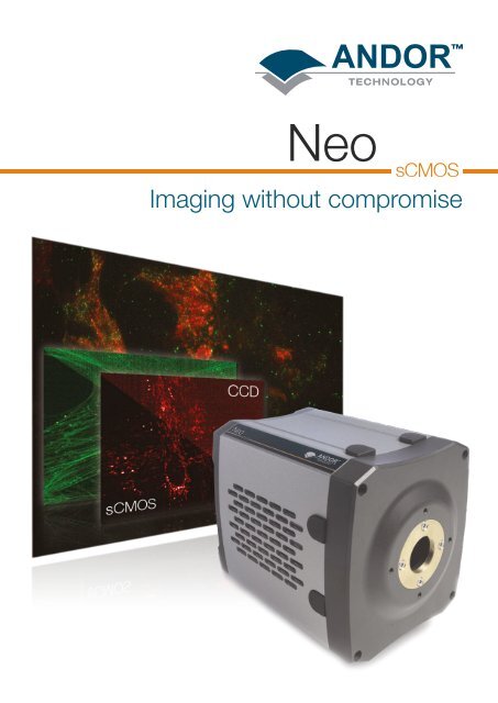
Imaging without compromise - Andor Technology
Imaging without compromise - Andor Technology
Imaging without compromise - Andor Technology

Create successful ePaper yourself
Turn your PDF publications into a flip-book with our unique Google optimized e-Paper software.
<strong>Imaging</strong> <strong>without</strong> <strong>compromise</strong>
Scientific CMOS (sCMOS)technology overviewScientific CMOS (sCMOS) is a breakthrough technology that offers an advanced set ofperformance features that render it ideal to high fidelity, quantitative scientific measurement.Scientific CMOS (sCMOS) can be considered unique in its ability to simultaneously deliver on many key performanceparameters, overcoming the ‘mutual exclusivity’ associated with current scientific imaging technology standards, anderadicating the performance drawbacks traditionally associated with CMOS imagers.sCMOS is uniquely capable of simultaneously delivering:• Extremely low noise• Rapid frame rates• Wide dynamic range• High resolution• Large field of view• High Quantum Efficiency (QE)• Rolling and Global (Snapshot) exposure modesDerek Toomre, PhD., AssociateProfessor, Department of Cell Biology,Yale University School of Medicine“Neo cameras will literally allow one to see cells in a new light withultra sensitive imaging at speeds never achieved before - as wehave seen in our tests of vesicle trafficking. These scientific CMOScameras are not a small step, but a quantum leap, that will open upnew possibilities of what can be studied in fast cellular processes,rapid screening, and super-resolution imaging.”sCMOS - No need to <strong>compromise</strong>The 5.5 megapixel sensor offers a large field of view and high resolution, <strong>without</strong>compromising read noise, dynamic range or frame rate. Rolling and Global (Snapshot)shutter readout ensure maximum application flexibility.Read noise is exceptional, even when compared to the highest performance ‘slow-scan’ CCDs. The fact that the sCMOSdevice can achieve 1 electron rms read noise while reading out 5.5 megapixels at 30 fps renders it truly extraordinary in themarket. Furthermore, the sensor is capable of achieving 100 full fps with a read noise 1.3 electrons rms. By way of comparison,the lowest noise Interline CCD, reading out only 1.4 megapixels at ~ 16 fps would do so with ~ 10 electrons read noise.The low noise readout is complemented by 30,000:1 dynamic range. Usually, for CCDs or EMCCDs to reach their highestdynamic range values, there needs to be a significant <strong>compromise</strong> in readout speed, yet sCMOS can achieve this value whiledelivering high frame rates. The unique dual amplifier architecture of sCMOS allows for high dynamic range by offering a largewell depth, despite the relatively small 6.5 µm pixel size, alongside lowest noise. A 1.4 megapixel Interline CCD with similarlysmall pixels achieves only ~1,800:1 dynamic range at 16 fps.Parameter sCMOS (Neo) Interline CCD EMCCDSensor Format 5.5 megapixel 1.4 to 4 megapixel 0.25 to 1 megapixelPixel Size 6.5 µm 6.45 to 7.4 µm 8 to 16 µmRead NoiseFull Frame Rate (max.)1 e - @ 30 fps1.4 e - @ 100 fpsSustained: >30 fps full frameBurst: 100 fps full frame4 - 10 e - < 1e - (with EM gain)3 to 16 fps ~ 30 fpsQuantum Efficiency (max.) 57% 60%90% ‘back-illuminated’65% ‘virtual phase’Dynamic Range30,000:1(@ 30 fps)~ 3,000:1(@ 11 fps)8,500:1(@ 30 fps withlow EM gain)Multiplicative Noise None None1.41x with EM gain(effectively halves the QE)SpeedResolutionDynamicRangeSee page 30 for‘Comparing sCMOS withother detectors’technical noteField ofViewSensitivityPage 2 Page 3
Performance and InnovationsLowest Noise Floor<strong>Andor</strong>’s ultrasensitive Neo sCMOS camera has broken new ground in offering anunparalleled 1 electron rms read noise floor, <strong>without</strong> amplification technology.What is truly extraordinary is that this performance level isachievable at 30 fps, representing 200 MHz pixel readoutspeed. Furthermore, even at full readout speed, the readnoise floor is negligibly <strong>compromise</strong>d, maintaining 1.3 e - rmsat 100 fps. For the best CCD cameras to even approach2 electrons noise, a readout speed of 1 MHz or sloweris required. This minimal detection limit renders the NeosCMOS suitable for a wide variety of challenging low lightimaging applications.See page 28 for‘Understanding Read Noise’technical noteReadout Speed (MHz) Readout Noise (e - )Rolling Shutter Global Shutter200 MHz 1 2.3560 MHz 1.3 2.5Extended Dynamic RangeThe <strong>Andor</strong> Neo is designed to make use of the innovative dual ‘column-level’ amplifierdesign of the sensor.Traditionally, sensors require that the user must select upfront between high or low amplifier gain (i.e. sensitivity) settings,depending on whether they want to optimize for low noise or maximum well depth. The dual amplifier architecture of thesCMOS sensor in Neo circumvents this need, in that signal can be sampled simultaneously by both high and low gainamplifiers. As such, the lowest noise of the chip can be harnessed alongside the maximum well depth, affording widestpossible dynamic range of up to 30,000:1.Dual Amplifier Architecture:Each column within each half of the sensor is equipped with dual column level amplifiers and dual analog-to-digitalconverters (ADC).This architecture was designed to simultaneously minimize read noise and maximize dynamic range. The dual columnlevel amplifier/ADC pairs have independent gain settings, and the final image is reconstructed by combining pixelreadings from both the high gain and low gain readout channels to achieve an unprecedented intra-scene dynamic rangefrom the relatively small 6.5 µm pixel pitch.High contrast image recorded with dual amplifier 16-bit mode of Neo(a)Neo sCMOSInterline CCDComparative low light images taken withNeo sCMOS (1.3 electrons read noise @560 MHz) vs Interline CCD (5 electronsread noise @ 20 MHz), displayed with samerelative intensity scaling(a) LED signal in a light-tight imagingenclosure, intensity ~ 30 photons/pixel;(b) Fluorescently labelled fixed cell using aCSU-X spinning disk confocal microscope(x60 oil objective), each 100 ms exposure,same laser power,Pixels sampled by high gainamplifier (~800 counts )Pixels sampled by low gainamplifier (~8,000 counts )See page 20 for‘Dual Amplifier Dynamic Range’technical note(b)Neo sCMOSInterline CCDSpurious Noise FilterNeo comes equipped with anoptional in-built FPGA filter thatoperates in realtime to reduce thefrequency of occurrence of highnoise pixels that would otherwisewould appear as spurious ‘salt andpepper’ noise spikes in the imagebackgroundNeo sCMOS cameras mounted on the <strong>Andor</strong>TuCam Dual Camera Image SplitterPage 6 Page 7
Performance and InnovationsRolling and Global (Snapshot) Shutter modesNeo offers the distinct capability to offer both Rolling Shutter and Snapshot exposuremodes from the same sensor, such that the most appropriate mode can be selecteddependent on application requirements.Rolling shutter essentially means that different lines ofthe array are exposed at different times as the read out‘waves’ sweep through the sensor. The fastest framerates are available from this mode.Rolling Shutter exposure and readout (single scan)Global shutter, which can also be thought of as a‘snapshot’ exposure mode, means that all pixels of thearray are exposed simultaneously, providing a ‘freezeframe’ capability that emulates an interline CCD.Global Shutter exposure and readout (single scan)Neo sCMOS Software Solutions<strong>Andor</strong> SolisSolis is a ready to run Windows package with richfunctionality for data acquisition and image analysis/processing.<strong>Andor</strong> Basic provides macro language control of dataacquisition, processing, display and export.<strong>Andor</strong> SDKA software development kit that allows you tocontrol the <strong>Andor</strong> range of cameras from your ownapplication. Available as 32 and 64-bit libraries forWindows (XP, Vista and 7) and Linux. Compatiblewith C/C++, C#, Delphi, VB6, VB.NET, LabView andMatlab.Exposure startExposureReadout Exposure start ExposureExposure End<strong>Andor</strong> iQSee page 26 for‘Rolling and Global (Snapshot)Exposure Capability’ technical noteComprehensive trigger functionalityNeo offers a selection of advanced trigger modes, designedto provide tight synchronization of the camera within a varietyof experimental set-ups. Triggering is compatible with bothRolling and Global shutter modes.• External TTL, Software and Internal trigger• Rolling and Global shutter trigger modes• ‘Time Lapse’ and ‘Continuous’ (overlapped) kinetic series• Rapid exposure switching (iCam)A comprehensive multi-dimensional imaging softwarepackage. Offers tight synchronization of EMCCD witha comprehensive range of microscopy hardware,along with comprehensive rendering and analysisfunctionality. Modular architecture for best price/performance package on the market.Bitplane ImarisImaris delivers all the necessary functionality forvisualization, segmentation and interpretation ofmultidimensional datasets.By combining speed, precision and intuitive ease-ofuse,Imaris provides a complete set of features forhandling multi-channel image sets of any size up to 50gigabytes.Trigger Mode Description Trigger sourcesTime LapseEach exposure started by a trigger event (e.g. TTL rising edge). Exposureduration is internally defined.Internal, External SoftwareThird Party Software CompatibilityThe range of third party software drivers for this new cameraplatform is expanding steadily. Please enquire for further details.ContinuousExposures run back to back with no time delay between them. Exposure timedefined by time between consecutive trigger events.Internal, ExternalExternal Exposure Exposure time defined by TTL width (sometimes known as ‘bulb mode’). ExternalExternal Start TTL rising edge triggers start of internally defined kinetic series. External trigger, followed byinternal timerAvailable Neo trigger modes applicable to both Rolling and Global shutterPage 14 Page 15
The <strong>Andor</strong> <strong>Imaging</strong> RangeHave you found what you are looking for? As an alternative to the Neo sCMOS, <strong>Andor</strong>offers an extensive portfolio of performance low light imaging camera technologies.iKon - deep cooled, low noise CCD• -100ºC coolingClara - high-performance interline CCDplatformLuca EM - price/performance EMCCDplatformiXon - high performance EMCCDplatform• Back-illuminated > 90% QE• Industry lowest read noise (2.4 e-)• Single photon sensitive• Single photon sensitive• 1 megapixel to 4 megapixel• -55ºC fan cooled; -40ºC vibration free mode• Compact• Industry fastest frame rates• Enhanced NIR versions• 1.4 megapixel• Luca R – megapixel format; 12.4 fps• -100ºC cooling• ‘PV Inspector’ model – optimized for EL/PLin-line inspection• USB 2.0 true plug and play• USB 2.0 true plug and play• USB 2.0 true plug and play• Flexible yet intuitive• Quantify in Electrons or PhotonsNeo – high performance Scientific CMOS (sCMOS)Dr. Yan GuConfocal <strong>Imaging</strong> and Analysis LabNational Institute for Medical Research• 1 electron read noise @ 30 fps• 5.5 Megapixel / 6.5 μm pixels• -40ºC cooling• Up to 100 fps• 4 GB on head memory• 16-bit data range‘We tested the <strong>Andor</strong> sCMOS camera in conjunction with a popular cooled CCD camera, and compared with results from a similar test of acompetitor’s scientific CMOS camera. <strong>Andor</strong>’s camera showed lowest dark noise, biggest field of view with very good sampling resolution(number of pixels), fastest frame rate, compatible signal to noise ratio and potentially largest dynamic range of detection. It is the most suitablecamera on the market for our project’Page 16 Page 17
Many optical configurations are sensitive to vibrations from thecamera fan, such as patch clamp or combined optical/AFM set-ups.The deep cooling advantage of Neo means that the internal fan can beturned off by instead opting to flow water through the convenientlylocated connections. <strong>Andor</strong>’s Neo offers:Exposure time: 1 s• Two fan speeds• Ability to turn off fan completely.‘Liquid cooling’ through the camera allows minimization of vibrationwhile still stabalizing at -40 °C.-40°C-30°C-15°C-5°C+5°CFigure 3 (a) – Blemishes at different temperatures for 1 sec exposure, as per current technical note.Exposure time: 30 ms+5°CFigure 2 - Thermal noise can sacrifice the sCMOS low detection limit. Low light images recorded with a Neo sCMOS at -30 °C versus acompeting sCMOS @ +5°C, Shown with same relative intensity scaling; 2 sec exposure time; 560MHz readout speed. Comparative lineintensity profiles from a single row is also shown for each case.-30°CFigure 3 (b) – Blemishes at -30°C vs +5°C for 30 msPage 24 Page 25
Technical NoteComparing sCMOS with other scientific detectorssCMOS technology is unique in its ability to overcome many of the mutual exclusivitiesthat have marred other scientific detector technologies, resulting in an imaging detectorthat simultaneously optimizes a range of important performance parameters whilstmaintaining snapshot exposure capability.Part 1 - Current scientific imagers: Interline CCD and EMCCDMany scientific imaging applications demand multi-megapixel focalplane sensors that can operate with very high sensitivity and widedynamic range. Furthermore, it is often desirable that these sensorsare capable of delivering rapid frame rates in order to capture dynamicevents with high temporal resolution. Often there is a strong elementof mutual exclusivity in these demands. For example, it is feasiblefor CCDs to achieve less than 3 electrons rms readout noise, but dueto the serial readout nature of conventional CCDs, this performancecomes at the expense of frame rate. This is especially true when thesensor has several megapixels of resolution. Conversely, when CCDsare pushed to faster frame rates, resolution and field of view aresacrificed (i.e. fewer pixels per frame to read out) or read noise anddynamic range suffer.By way of illustration, consider one of the most popular, highperformancefront-illuminated scientific CCD technologies on themarket today – the Interline CCD. These devices are capable ofreading out at 20 megapixel/s per output port with a respectable readnoise of only 5 to 6 electrons rms. At this readout speed a single port1.4 megapixel sensor can achieve 11 fps. Use of microlenses ensuresthat most of the incident photons are directed away from the Interlinemetal shield and onto the active silicon area for each pixel, resulting inpeak QE greater than 60%. High performance combined with low costhas made the Interline CCD a very popular choice for applicationssuch as fluorescence cell microscopy, luminescence detectionand machine vision. However, even 5 to 6 e - noise is too high formany low light scientific applications. For example, when imagingthe dynamics of living cells, there is a need to limit the amount offluorescence excitation light, such that both cell phototoxicity andphotobleaching of the fluorescent dyes is minimized. The use oflower power excitation results in a proportionally lower fluorescentemission signal from the cell. Also dynamic imaging yields shorterexposure times per frame, thus fewer photons per frame. Ultra lowlight conditions mean that the read noise floor can often become thedominant detection limit, seriously compromising the overall signalto-noiseratio (SNR) and hence the ability to contrast fine structuralfeatures within the cell. As such, the inability to maintain low noiseat faster readout speeds limits the overall flexibility of the InterlineCCD camera.The Electron Multiplying CCD (EMCCD) was introduced into themarket by <strong>Andor</strong> in 2000 and represents a significant leap forwardin addressing the mutual exclusivity of speed and noise as discussedabove. EMCCD cameras employ an on-chip amplification mechanismcalled ‘Impact Ionization’ that multiplies the photoelectrons that aregenerated in the silicon. As such, the signal from a single photonevent can be amplified above the read noise floor, even at fast, multi-MHz readout speeds. Importantly, this renders the EMCCD capableof single photon sensitivity at fast frame rates (e.g. 34 fps with a 512 x512 array). This attribute has rapidly gained recognition for EMCCDtechnology in demanding low light measurements, such as singlemolecule detection.However, despite the sensitivity under extremely low light conditions,there are a few remaining drawbacks of EMCCD technology. Theamplification mechanism required to reduce the effective read noiseto < 1e - , also induces an additional noise source called multiplicativenoise. This effectively increases the shot noise of the signal by afactor of 1.41, which is manifested as an increase in the pixel to pixeland frame to frame variability of low light signals. The net effectof multiplicative noise is that the acquired image has a diminishedsignal-to-noise ratio, to an extent that the QE of the sensor can bethought to have been effectively reduced by a factor of two. Forexample, a QE-enhanced back-illuminated EMCCD with 90% QEhas effectively 45% QE when the effects of multiplicative noiseare considered. Dynamic range limitations of EMCCDs must alsobe considered. It is possible to achieve respectably high dynamicrange with a large pixel (13 to 16 μm pixel size) EMCCD, but onlyat slow readout speeds. As such, higher dynamic range can onlybe reached at slower frame rates (or with reduced array size) withmodest EM gain settings. Application of higher EM gain settingsresults in the dynamic range being depleted further. Sensor cost ofEMCCD technology is an additional consideration, along with thepractical restriction on resolution and field of view that accompaniessensor cost. Presently, the largest commercially available EMCCDArray Size (H x V) Rolling Shutter mode (fps) Global (Snapshot) Shutter mode (fps)2560 x 2160 (full frame) 100 502064 x 2048 (4 megapixel) 104 521392 x 1040 (1.4 megapixel) 204 100512 x 512 412 200128 x 128 1,616 711Table 1 - Frame rate vs sub-window size; Rolling and Global shutter readout modes. N.B. Same sub-window frame rates apply when using fullhorizontal width with the vertical heights indicated (see body text for further detail).sensor is a back-illuminated 1024 x 1024 pixel device with 13 μmpixel pitch, representing a 13.3 x 13.3 mm sensor area. This alreadycarries a significant cost premium, making further expansion to multimegapixeldevices a costly proposition.Part 2 - sCMOS: Circumventing the trade-offsScientific CMOS (sCMOS) technology is based on a new generationof CMOS design and process technology. This device type carries anadvanced set of performance features that renders it entirely suitableto high fidelity, quantitative scientific measurement. sCMOS can beconsidered unique in its ability to simultaneously deliver on manykey performance parameters, overcoming the ‘mutual exclusivity’that was earlier discussed in relation to current scientific imagingtechnology standards, and eradicating the performance drawbacksPerformance highlights of sCMOS CIS 2051sensor:• Sensor format: 5.5 megapixels (2560(h) x 2160(v))• Read noise: 1 e - rms @ 30 fps;1.3 e - rms @ 100 fps• Maximum frame rate: 100 fps• Pixel size: 6.5 μm• Dynamic range: 30,000:1 (@ 30 fps)• QE max.: 57%• Read out modes: Rolling and Global shutter (user selectable)that have traditionally been associated with conventional CMOSimagers.The 5.5 megapixel sensor offers a large field of view and highresolution, <strong>without</strong> compromising read noise or frame rate. The readnoise in itself is exceptional, even when compared to the highestperformance CCDs. Not even slow-scan CCDs are capable of thislevel of read noise performance. High-resolution, slow-scan CCDsare typically characterized by seconds per frame rather than framesper second. The fact that the sCMOS device can achieve 1 electronrms read noise while reading out 5.5 megapixels at 30 fps renders ittruly extraordinary in the market. Furthermore, the sensor is capableof achieving 100 full fps with a read noise 1.3 electrons rms.By way of comparison, the lowest noise Interline CCD reading outonly 1.4 megapixels at ~ 16 fps would do so with ~ 10 electrons readnoise.Greater speed is available through selection of ‘region of interest’sub-windows, such that the field of view can be traded off to achieveextreme temporal resolution. Table 1 shows frame rates that can beexpected from a series of sub-window sizes, in both rolling shutterand global shutter modes of operation (the distinction between thesetwo modes is explained later in this paper). Note that each of the subwindowscan be expanded to full width in the horizontal direction andstill maintain the same indicated frame rate. For example, both 1390 x1024 and 2560 x 1024 sub-window sizes each offer 220 fps in rollingshutter mode. This is important information for some applicationsthat can take advantage of an elongated (letter box shape) region ofinterest.The low noise readout is complemented by a high dynamic rangeof 30,000:1. Usually, for CCDs or EMCCDs to reach their highestdynamic range values, there needs to be a significant <strong>compromise</strong> inreadout speed, yet sCMOS can achieve this value while delivering 30fps. Furthermore, the architecture of sCMOS allows for high dynamicrange by offering a large well depth, despite the small pixel size. Byway of comparison, a 1.4 megapixel Interline with similarly smallpixels achieves only ~1,800:1 dynamic range at 16 fps.Part 3 - Comparing sCMOS to other leading scientific imagingtechnologiesA short comparative overview of sCMOS is provided in Table 2. Forthe purposes of this exercise, we limited the comparison to InterlineCCD and EMCCD technologies, given their popularity across therange of scientific imaging applications. Interline CCDs are typifiedby a choice of 1.4 megapixel or 4 megapixel sensors. The mostpopular EMCCD sensors are 0.25 or 1 megapixel, typically offeringup to 30 fps.Parameter Neo sCMOS Interline CCD EMCCDSensor Format 5.5 megapixel 1.4 to 4 megapixel 0.25 to 1 megapixelPixel Size 6.5 μm 6.45 to 7.4μm 8 to 16 μmRead NoiseFull Frame Rate (max.)1 e - @ 30 fps1.3 e - @ 100 fpsSustained: >30 fps full frameBurst: 100 fps full frame4 -10 e - < 1e - (with EM gain)3 to 16 fps ~ 30 fpsQuantum Efficiency (QE) 57% 60% 90% ‘back-illuminated’65 % ‘virtual phase’Dynamic Range 30,000:1(@ 30 fps)~ 3,000:1(@ 11 fps)8,500:1(@ 30 fpswith low EM gain)Multiplicative Noise none none 1.41x with EM gain (effectivelyhalves the QE)Table 2 - Comparison summary of typically specifications of Interline CCD and EMCCD technologies compared to sCMOS technology.Page 30 Page 31
It is apparent that across most parameters, sCMOS presents a distinctperformance advantage, notably in terms of noise, speed, dynamicrange and field of view/resolution. Importantly, these advantages aremet largely <strong>without</strong> <strong>compromise</strong>. Whilst the read noise of sCMOS isvery low, EMCCD technology still maintains the distinct advantageof being able to multiply the input signal above the read noise floor,thus rendering it negligible (
sCMOS (1.2 e - noise)Interline CCD (5 e - read noise)5.5 Megapixel sCMOS1.4 Megapixel Interline CCDFigure 4 - Comparative low light fluorescencemicroscopy images taken with <strong>Andor</strong> sCMOS (1.3 e - @560 MHz) vs Interline CCD (5 e - @ 20 MHz) under lowlight conditions, typical of those employed in dynamiclive cell imaging. ND filters on a widefield fluorescencemicroscope were used to reduce light levels relative tothe read noise floor.Figure 7 - Field of view comparison of twotechnologies; x60 magnification; 1.25 NA; 5.5megapixel <strong>Andor</strong> sCMOS vs 1.4 megapixel InterlineCCD (each have ~ 6.5 μm pixel pitch). sCMOS iscapable of offering this larger field of view @ 100frame/s with 1.3 e - read noise.5.5 Megapixel sCMOS1.4 Megapixel Interline CCDFigure 5 - Theoretical Signal to Noise plotcomparisons for sCMOS vs Interline CCD sensors.Photon flux (i.e. input light intensity) is given in termsof photons per 6.5 μm pixel of each sensor type.sCMOSInterline CCDFigure 6 - Theoretical Signal to Noise plotcomparisons for sCMOS vs Interline CCD vs backilluminatedEMCCD sensors. For purposes of aobjective comparison, it is assumed that the ~6.5 μmpixels of the sCMOS and Interline CCD sensors are 2x 2 binned in order to equal a 13 μm pixel of a backilluminatedEMCCD.Figure 8 - Field of view and resolution comparison oftwo technologies; x100 magnification; 1.45 NA; 5.5megapixel <strong>Andor</strong> sCMOS vs 1.4 megapixel InterlineCCD (each have ~ 6.5 μm pixel pitch).Page 34 Page 35
Technical NoteNeo sCMOS Data Flow Considerations andPC RecommendationsThe Neo sCMOS camera is capable of sustained data rates that are markedly faster thanother scientific cameras on the market. The full frame rate pixel readout speed of 560 MHzyields a data rate of ~ 840 MB/sec (single amplifier mode); ~ 1120 MB/sec (dual amplifiermode).(a) Using Neo on-head memoryNeo sCMOS is equipped with 4 GB of on-head memory buffer, throughwhich data is flowed. This buffer can be used to burst data to until full,even at maximum frame rate of the camera. Frames will enter andleave this memory buffer continuously, but the speed of transfer to PCwill be dictated by either Cameralink interface bandwidth or hard drivewrite speed (if hard disk spooling is selected), alongside any otherassociated ‘handshaking’ or ‘processing’ overheads associated withthe acquisition software. The severity of the data transfer bottleneck(i.e. the rate that data can leave the camera memory) therefore dictatesexactly how many frames in a kinetic series can be recorded to cameramemory buffer before it becomes full.In reality, one might expect capacity for between 400 to 500 frameswhen operating at 100 fps, 5.5 megapixel (full resolution) in singleamplifier mode (11-bit). In other words, the buffer can hold 4 to 5seconds worth of kinetic series data under maximum frame rateconditions of the camera. If a smaller ROI size is selected, one hasthe option to either (a) maintain frame rate and extend kinetic serieslength beyond 5 seconds, or (b) achieve faster frame rates but staywithin the 4 to 5 sec threshold.(b) Data spooling – awareness of the ‘bottlenecks’Some applications require kinetic series lengths that significantlyexceed 5 seconds. In such cases, the data must be spooled continuouslyto either a PC hard drive or PC RAM with greater than 4 GB capacity.The data transfer rates achievable over more extended kinetic seriesare limited either by the data bandwidth of the Cameralink interfacebetween camera and PC or by the hard drive write speed (if spooling tohard drive is selected). The maximum sustained speeds are ultimatelylimited by the interface bandwidth in addition to time taken for a ‘readrequest’ to be sent by the software to retrieve the next image. Thesingle cameralink interface (‘3-tap’) has a bandwidth limitation of ~250 MB/sec, which translates to ~ 30 fps of 5.5 MP image size, singleamplifier dynamic range mode. Thus, to achieve maximum availablesustained speeds, a PC configuration should be capable of writing/spooling data at faster than this rate (see section D).The maximum length of a kinetic series is determined by the capacityof PC RAM or hard drive that is assigned for spooling. The issue ofdetermining achievable speeds is further compounded by the fact thatdata rates are also adjusted by user selected variables such as exposuretime, pixel readout speed, ROI size, hardware binning or single/dualamplifier dynamic range modes.(c) Dataflow MonitorIn order to better estimate any limitations of system bottleneckson a requested kinetic series, <strong>Andor</strong> have developed the Dataflowmonitor for Neo, accessible through the set-up dialogue of the Solisacquisition software. This will provide ‘up-front’ information onwhether the kinetic series conditions that have been requested by theuser are likely to compatible or incompatible with the data transferand write bandwidths available from Cameralink interface and PChard drive respectively.The Dataflow monitor will also estimate the available storage capacityof camera, PC RAM or hard drive to determine whether the length ofrequested kinetic series is within storage limits. This should betterinform the user of potential data speed or capacity complications inadvance of beginning an acquisition. Figure 1 below illustrates ascenario in which the Dataflow monitor has accepted and flagged akinetic series request, respectively.Figure 1 - The Dataflow monitor has raised a warning against therequested kinetic series. In this case the data rate exceeds that ofthe hard drive write speed. Options are to rectify include: (a) reduceframe rate / lengthen exposure time (b) reduce ROI size (c) usehardware binning (d) use single amplifier mode (d) reduce kineticseries length to be within the 4 GB on-head camera memory (e) spoolto PC RAM (if greater than 4 GB).(d) Speed tests1 - ‘Extended’ kinetic series testsTable 1 outlines some PC solutions for Neo sCMOS that were in-housetested by <strong>Andor</strong> over extensive kinetic series lengths. The test utilisedSolis acquisition software, internal triggered, rolling shutter mode and560MHz pixel readout speed, in both 11 bit (single amplifier) and16-bit (dual amplifier) data range configurations. The results indicatefor each system configuration the frame rates achieved over very longkinetic series lengths, spooling to either hard drive (systems A and B)or PC RAM (system C).• Each PC configuration is based on the same ‘base’ system, which isa Dell T5500 with 2.6 GHz Quad Core. For each system one of theavailable hard drives is assigned to the operating system (Windows 7),the remaining drives configured in RAID 0 for fast data spooling.• The speed tests represented in table 1 were tested using extensivekinetic series lengths of several thousand frames:• 2560 x 2160 – 6,000 frames (except System C)• 2048 x 2048 – 6,000 frames (except System C with 16-bit range)• 1396 x 1024 – 8,000 frames• 512 x 512 – 10,000 frames• 128 x 128 – 15,000 frames• System A makes use of the RAID 0 dual hard drives for directspooling.• System B utilizes 3x 15K 600 GB SAS hard drives configured inRAID 0 for data spooling (an additional fourth hard drive assigned tothe operating system)System AIntermediate Speed(RAID HD)* Series length limited by storage capacity of RAMDISK (44 GB allocated)• System C utilizes 48 GB of PC RAM for direct spooling. Solisacquisition software is a 32-bit application and thus a RAMDISKapplication was utilised to ‘effectively’ convert RAM into a fast spoolhard drive that is not limited to 4GB blocks. 44 GB were allocatedfor this purpose. Note, the RAMDISK would not be required with a64-bit acquisition engine, such as the <strong>Andor</strong> SDK. Note also that 3xSATA drives are maintained as fast transfer storage drives.System BMaximum Speed(RAID HD)System CMaximum Speed(RAM)Platform Dell T5500 Dell T5500 Dell T5500Processor 2.6 GHz Quad Core 2.6 GHz Quad Core 2.6 GHz Quad CoreMemory 4 GB 4 GB 48 GBHard drives 3 x 10K 600 GB SATA 4 x 15K 600 GB SAS 3 x 10K 600 GB SATAArray size /ROIData Range Frame Rate Series length Frame Rate Series length Frame Rate Series length2560 x 2160 11-bit 23 fps 6,000 32.5 fps 6,000 32.5 fps 5,200*(full resolution) 16-bit 18 fps 6,000 24.5 fps 6,000 24.5 fps 4,000*2048 x 2048 11-bit 30 fps 6,000 40.5 fps 6,000 40.5 fps 6,00016-bit 22.5 fps 6,000 32 fps 6,000 32 fps 5,200*1396 x 1024 11-bit 62 fps 8,000 83 fps 8,000 83 fps 8,00016-bit 47 fps 8,000 83 fps 8,000 83 fps 8,000512 x 512 11-bit 125 fps 10,000 181 fps 10,000 181 fps 10,00016-bit 94 fps 10,000 181 fps 10,000 181 fps 10,000128 x 128 11-bit 530 fps 15,000 1098 fps 15,000 1087 fps 15,00016-bit 395 fps 15,000 1098 fps 15,000 1087 fps 15,000Table 1 - Frame rates achieved by Neo for 3 different PC configurations, tested over kinetic series lengths of between 6,000 and 10,000 frames,significantly exceeding the 4 GB on-head memory buffer of the Neo camera.Page 36 Page 37
2 - ‘Sustained’ kinetic series testsThe speeds represented in table 1, while achievable over extensivekinetic series lengths that would satisfy the majority of applications,still cannot be thought of as representing the true ‘sustained’ framerate capability. In fact, in the figure 1 tests, the 4 GB on-head memorybuffer was still being very gradually filled as frames entered the bufferslightly faster than being retrieved from the buffer by the software.As such, if the kinetic series lengths had been pushed to significantlygreater than those represented, the series would have failed due to thememory buffer becoming full.Table 2 shows data that can be considered indicative of sustainedframe rates, the kinetic series lengths limited only by the storagecapacity of the RAM or hard disk to which data is being spooled.The table was generated by a method that measures how fast framesare retrieved by the <strong>Andor</strong> SDK, that being the rate limiting step forsustained measurement. ‘System C’ was used for this test, the dataspooled to the 48 GB RAM.Array size / ROI Data Range Frame Rate2560 x 216011 bit 30.8 fps(full resolution) 16 bit 23.2 fps2048 x 2048 11 bit 38.9 fps16 bit 30.7 fps1396 x 1024 11 bit 75 fps16 bit 75 fps512 x 512 11 bit 152 fps16 bit 152 fps256 x 256 11 bit 301 fps16 bit 301 fps128 x 128 11 bit 592 fps16 bit 592 fpsTable 2 - Sustained frame rates achieved by Neosent images into the 4 GB buffer. Over time this will gradually fillup as images are only being retrieved from the buffer by the SDK/software at a rate of 28 fps. Under these conditions, if a kinetic serieslength significantly greater than 6,000 frames had been specified, thekinetic series would not have completed due to the memory bufferfilling up.Appendix• Both SDK 3 and Solis are compatible with a 64-bit OS. Notehowever that iQ software requires a 32-bit OS• 64-bit 3 rd party software packages must use the 64-bit SDK3 andoperate on 64-bit OS• 64-bit software can spool directly to PC RAM• RAMDISK is the ONLY way to make use of > 4 GB PC RAM ina 32-bit application• <strong>Andor</strong>’s only tested RAMDISK solution can be accessed throughthis link:SuperSpeed LLCRamDisk Plus 10.x (32 bit)www.superspeed.comNotes...From an SDK integration and driver development standpoint, it isimportant to note that the frame rates given in table 2 relate to howrapidly data can be retrieved from the camera. However, additionalprocessing overheads, including saving data to the hard drive, couldimpact these figures.3 - Comparing ‘Extended’ to ‘Sustained’It is evident that the frame rates attainable for a kinetic series of upto 6,000 frames (full resolution) are slightly faster than frame ratesattained over ‘sustained’ (limited only by capacity of spool drive/RAM) kinetic series conditions, i.e. 32.5 fps vs 30.8 fps.The reason behind this observation can be understood as follows:The true sustained frame rate is dictated by the rate that images canbe retrieved by SDK/software – a cycle here is made up by the timetaken to transfer an image through the Cameralink interface, plus thetime taken for a read request to be sent back to camera (‘handshakingoverhead’), corresponding to a frame rate of 30.8 fps (full frame).The frame rate can be pushed faster when we make use of the 4 GBmemory buffer, as in the case of the 6,000 frame example given intable 1. In this instance, the camera acquired at a rate of 30.8 fps andPage 38Page 39
Notes...Notes...Page 40Page 41
Prof Amit MellerAssociate Professor of BiomedicalEngineering and Physics,Boston University“Our tests with <strong>Andor</strong>’s new sCMOS camera have been highlyencouraging. The combination of very low noise sensitivity at rapidframe rates, coupled with high pixel resolution, will enable us toreach previously unattainable throughput from our massively parallel,nanopore-based, single molecule sequencing approach.”Neo sCMOS Quantum Efficiency (QE)curve, incorporating laser excitationlines and emission ranges of commonfluorophore labels.Front cover image:Mouse embryonic fibroblast cellstransfected with DNA plasmids,encoding for two fluorescentproteins: clathrin, fused to greenfluorescent protein (GFP-Clathrin),and Rab5, fused to the monomericred fluorescent protein (mRFP-Rab5),imaged by total internal reflectionfluorescence microscopy. GFP-clathrin localizesto vesicles that form on the plasma membraneof cells (visible as green spots). mRFP-Rab5 isfound on vesicles located more internally, but stillwithin the evanescent field generated by totalinternal reflection fluorescence (red spots).Image courtesy of Dr. Roberto Zoncu, WhiteheadInstitute for Biomedical Research, MIT.Page 42Page 43
<strong>Andor</strong> Customer Support<strong>Andor</strong> products are regularly used in critical applications and we can provide avariety of customer support services to maximise the return on your investmentand ensure that your product continues to operate at its optimum performance.<strong>Andor</strong> has customer support teams located across North America, Asia andEurope, allowing us to provide local technical assistance and advice. Requestsfor support can be made at any time by contacting our technical support team atandor.com/support.<strong>Andor</strong> offers a variety of support under the following format:• On-site product specialists can assist you with the installation andcommissioning of your chosen product• Training services can be provided on-site or remotely via the Internet• A testing service to confirm the integrity and optimize the performance ofexisting equipment in the field is also available on request.A range of extended warranty packages are available for <strong>Andor</strong> products giving youthe flexibility to choose one appropriate for your needs. These warranties allow youto obtain additional levels of service and include both on-site and remote supportoptions, and may be purchased on a multi-year basis allowing users to fix theirsupport costs over the operating lifecycle of the products.Project part financed by the European Regional Development Fund under the European Sustainable Competitiveness Programme forNorthern Ireland.Head Office7 Millennium WaySpringvale Business ParkBelfast BT12 7ALNorthern IrelandTel: +44 (28) 9023 7126Fax: +44 (28) 9031 0792North America425 Sullivan AvenueSuite 3South Windsor, CT 06074USATel: +1 (860) 290 9211Fax: +1 (860) 290 9566Japan4F NE Sarugakucho Building2-7-6 Sarugaku-ChoChiyoda-KuTokyo 101-0064JapanTel: +81 (3) 3518 6488Fax: +81 (3) 3518 6489ChinaRoom1213, Building BLuo Ke Time SquareNo. 103 HuizhongliChaoyang DistrictBeijing 100101ChinaTel: +86 (10) 5129 4977Fax: +86 (10) 6445 5401NB 0112