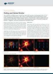
iStar ICCD Brochure - Andor Technology
iStar ICCD Brochure - Andor Technology
iStar ICCD Brochure - Andor Technology

You also want an ePaper? Increase the reach of your titles
YUMPU automatically turns print PDFs into web optimized ePapers that Google loves.
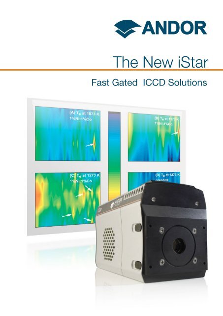
The New <strong>iStar</strong>Fast Gated <strong>ICCD</strong> Solutions
FeaturesUSB 2.0 connectivityBenefitsIndustry-standard plug-and-play, lockable and rugged interfaceSeamless multi-camera control from single PC or laptop.The New <strong>iStar</strong> –Scientific-grade Intensified CCDs from <strong>Andor</strong> <strong>Technology</strong>Fast gated <strong>ICCD</strong>sBuilding on more than 16 years of Excellence in the development of worldclass,fast-gated Intensified CCD cameras (<strong>ICCD</strong>), <strong>Andor</strong> redefines thestandard of rapid, nanosecond time-resolved imaging and spectroscopywith the introduction of the New <strong>iStar</strong> family.<strong>Andor</strong>’s <strong>iStar</strong> extracts the very best from CCD sensor and gated image intensifiertechnologies, achieving a superior combination of rapid acquisitions rates and ultra-highsensitivity down to single photon. Exceptional detection performances are accessedthrough high quantum-efficiency image intensifiers, thermo-electric cooling to -40ºC,500 kHz photocathode gating rates and enhanced intensifier EBI noise reduction.Low jitter, low insertion delay gating electronics and nanosecond-scale optical gatingprovide excellent timing accuracy down to a few 10’s of picoseconds, allowing ultra-precisesynchronization of complex experiments through <strong>iStar</strong>’s comprehensive range ofinput/output triggering options.5 MHz readout platform Rapid frame and spectral rates for superior characterization ofdynamic phenomena.Single readout amplifier for best image digitization uniformity.Comprehensive binning options -Crop & Fast Kinetic modeHigh-resolution sensors and imageintensifiersHigh QE Gen 2 & 3 image intensifiersTrue optical gating < 2 nsLow jitter, on-board Digital Delay Generator(DDG TM )Insertion delay as low as 19 nsComprehensive triggering interfaceIntelligate TMFully software-customizable binning sequences for highestspectral and image rates.Greater than 6,667 spectra/s continuous rates, up to55,250 spectra/s in burst mode.Sharpest images and spectrum definition, 100% fill factor formaximum signal collection efficiency.Superior photon capture, with peak QE up to 50% and spectralcoverage from 120 to 1,100 nm.Billionth of a second time-resolution for accurate transientphenomena study.Highest gating timing accuracy with lowest propagation delay.Minimum delay between experiment signal generation and actualimage intensifier triggering.Software-controlled 3x triggering outputs with 10 ps setupaccuracy for complex experiment integration.Intelligent and accurate MCP gating for better than 1:10 8 shutteringefficiency in the UV.500 kHz sustained photocathode gating Maximizes signal-to-noise ratio in high repetition rate laser-basedapplications.Photocathode EBI minimizationTE-cooling to -40ºCReal-time control interfaceDry gas purge interface for further efficient EBI reduction.Efficient minimization of CCD dark current and pixel blemishes.On-the-fly software control of intensifier gain, gating and3x outputs trigger parameters for real-time detection optimization.2 year warranty Reliability and guaranteed performance.The New <strong>iStar</strong> stands for...High sensitivityRapid spectral andimaging ratesHighest timing resolutionand accuracyMost compact designEase of integrationEase of use“Kinetics investigation of a laser-induced ablation plumeof mercury as a nonlinear medium for Vacuum UltraVioletgeneration”Courtesy of Laurent Philippet, Laboratoire de Physique desLasers, CNRS, Paris 13 UniversityApplication focus• Plasma studies• Laser Induced Fluorescence (LIF / PLIF)• Time-resolved luminescence& photoluminescence• Laser Induced BreakdownSpectroscopy (LIBS)• Transient absorption• Combustion StudiesUser publication database atandor.com/spectroscopyPage 2 Page 3
320T340TTen reasons to choosethe New <strong>iStar</strong>High resolution spectroscopy and imaging sensorsThe New <strong>iStar</strong> family features a range of high resolutionsensors for the sharpest nanosecond time-resolved imagesand spectral signatures acquisition, with no compromisein collection efficiency. All sensors feature pixels exhibiting100% fill factor, unlike microlense-less interline sensorswhere ~ 50% of the incoming signal will be blocked.High well-depth options – i.e. 312T and 320T platforms– also offer greater dynamic range for applications suchas Transient Absorption or Plasma Spectroscopy with abroad range of spectral features intensity. All CCDs in theNew <strong>iStar</strong> platform are Front-Illuminated types, and usea fibre-coupling arrangement to the image intensifiersfor maximum collection efficiency, unlike lens-coupledconfigurations that would suffer from lower throughput,image vignetting and distortion.ImageintensifierImaging platforms 312T 334TFibre-opticCouplerCCDArray format 1024 x 255 2048 x 512Pixel size 26 x 26 μm 13.5 x 13.5 μmEffective area(vs. imageintensifier Ø)RecommendedapplicationsØ 18 mm intensifier18 x 6.6 mmØ 25 mm intensifier25 x 6.6 mmRapid, broadband spectroscopyUltrafast, broadband multi-track spectroscopyDriving the absolute best acquisition speedØ 18 mm intensifier18 x 6.9 mmØ 25 mm intensifier25 x 6.9 mmHigh resolution, broadband spectroscopyBroadband, multi-track spectroscopyThe 5 MHz digitization and microsecond-range vertical clock shift speeds extract the very best frame rate and spectral ratefrom these sensors, providing outstanding rapid transient phenomena study capabilities.312T 320T 334T 340TSensor array size 512 x 512 1024 x 255 1024 x 1024 2048 x 512Pixel size 24 x 24 µm 26 x 26 µm 13 x 13 μm 13.5 x 13.5 µmMax. readout speed 5 MHz 5 MHz 5 MHz 3 MHzFrame rates1x1 full frame 15.8 fps 15.9 fps 4.2 fps 2.5 fps2x2 binning 28.5 fps 28.9 fps 7.3 fps 5.6 fpsSpectral rates (FVB) 291 sps 323 sps 145 sps 135 spsArray format 512 x 512 1024 x 1024Pixel size 24 x 24 μm 13 x 13 µmEffective area(vs. imageintensifier Ø)IntensifierØ 18 mm intensifier12.3 x 12.3 mmØ 18 mm intensifier13.3 x 13.3 mm1995 - InstaSpec VFirst ultra-compact Research <strong>ICCD</strong> withon-board gain control for time-resolvedimaging and spectroscopy.View our user publications database atandor.com/publicationsCCD2000 - <strong>iStar</strong>RecommendedapplicationsUltrafast, high dynamic range imagingUltrafast, narrowband spectroscopyUltra-fast kinetics & multi-trackHigh resolution imagingHigh resolution, narrowband spectroscopyExtended fast kinetics series & multi-trackFirst scientific-grade <strong>ICCD</strong> with on-board,fully integrated digital delay generator (noexternal controller), MCP gating for enhancedon/off ratio in the UV, ‘Gen 3’ film-lessintensifiers and single window design formaximum throughput.CCDInterline (no microlense)100% fill factor pixel =maximum collectionVs.50% fill factor pixel =50% lower collection2011 - New <strong>iStar</strong>First USB 2.0 <strong>ICCD</strong> with 2 nd generation ofon-board DDG for enhanced interfacingfunctionalities and timing accuracies.Fastest platform with deepest TE coolingfor high sensitivity, time-resolvedspectroscopy.PixelCCD fibre-optic platePage 4 Page 5
Crop mode: Pushing frame and spectral rate further...... and beyond with fast kinetic modeThis readout mode uses the actual sensor as a temporary storage medium, allowing extremely fast sequencesto be captured. By using the fastest vertical clock speeds as advised by the manufacturer, the New <strong>iStar</strong>achieves the highest sustained aquisition rates on the market.The active imaging area of the sensor is defined in a way thatonly a small section of the entire chip is used for imaging orspectral acquisition.T1) CCD “Keep Clean” sequence is interrupted, anduseful signal builds-up on the user-defined top portionof a sensorThe remaining area has to be optically masked to prevent lightleakage and charge spill-over that would compromise the signalfrom the imaging area.T2) At the end of the exposure time, signal is rapidlyshifted down by a pre-defined number of rows, and asecond exposure takes placeBy cropping the sensor, one achieves faster frame and spectralrates because the temporal resolution will be dictated only by thetime it requires to read out the small section of the sensor.T3) This process is repeated until the number ofacquisitions equals the series length set by userT4) The sequence moves into the readout phase byshifting in turn the individual acquisitions to the readoutregister, which is then read outT1)T2)T3)T4)312T 320T 334T 340TSensor array size 512 x 512 1024 x 255 1024 x 1024 2048 x 512Pixel size 24 x 24 µm 26 x 26 µm 13 x 13 μm 13.5 x 13.5 µmMax. readout speed 5 MHz 5 MHz 5 MHz 3 MHzCrop mode rates (imaging) 1,031 fps 526 fps 333 fps 184 fps[number of rows equivalent to a130 µm high channel][5 rows] [5 rows] [10 rows] [10 rows]Crop mode rates (spectral, binned) 6,667 sps 3,571 sps 3,450 sps 1,825 sps[number of rows equivalent to a130 µm high channel][5 rows] [5 rows] [10 rows] [10 rows]Even lower vertical clock shift speeds are available on the New <strong>iStar</strong>, but may yield to loss of well-depth and Charge TransferEfficiency (CTE, i.e. smearing). The New <strong>iStar</strong> offers a unique software-controlled clock amplitude adjustment to compensatefor these drawbacks.312T 320T 334T 340TSensor array size 512 x 512 1024 x 255 1024 x 1024 2048 x 512Pixel size 24 x 24 µm 26 x 26 µm 13 x 13 μm 13.5 x 13.5 µmMax. readout speed 5 MHz 5 MHz 5 MHz 3 MHzFast kinetics rates vs.channel heights26 µm 86,210 Hz[1 row]37,990 Hz[1 row]48,780 Hz[2 rows]30,030 Hz[2 rows]Different platforms for different time resolution needs50 µm 55,250 Hz[2 rows]100 µm 32,150 Hz[4 rows]26,590 Hz[2 rows]16,615 Hz[4 rows]29,850 Hz[4 rows]16, 805 Hz[8 rows]16,920 Hz[4 rows]10,225 Hz[8 rows]200 µm 17, 510 Hz[8 rows]9,495 Hz[8 rows]9,525 Hz[15 rows]4,975 Hz[15 rows]Lowest sensor dark currentOne would intuitively think that dark current in <strong>ICCD</strong>s is not typically an issue, as intensifier gain can beapplied to overcome this noise prior to reaching the CCD, and time scales involved - e.g. the nanosecondscale – mean that very little CCD dark current will build-up.So for which scenarios is extreme dark current essential?Check out the <strong>Andor</strong> website for more informationon all Spectroscopy and Imaging platformsandor.comExperiments involving multi-kHz lasers and extremely weak sampleemission, where multiple photocathode gatings can be set within a singleCCD exposure. This exposure is typically set to a few seconds to allow forhundreds of thousands of accumulations to occur. During these extendedCCD exposures, sensor deep cooling is of the greatest importance.Photon counting, where any noise contribution from any element of the<strong>ICCD</strong> has to be minimized to allow access to the lowest detection threshold.As Image Intensifiers are fibre coupled to the CCD, the photocathode willsee some degree of conductive cooling, which will contribute to minimizethe EBI. Further thermal noise reduction can be achieved through the <strong>iStar</strong>’sdry gas purge interface.Page 6 Page 7
Pushing the limits of nanosecond time-resolved detectionOriginally develop for night vision applications, image intensifiers can also act as ultra-fast (nanosecond-scale) optical shutters,as well as provide signal amplification up to x1,000 proved invaluable in the world of research for studies of short-lived events,e.g. fluorescence decay time measurements, or ultrafast dynamic behaviour studies, e.g. plasma or combustion kinetics.The response of an <strong>ICCD</strong> is governed by the Quantum Efficiency (QE) of the intensifier tube, which is determined by thecombination of the input window and the photocathode. The input window usually determines the lower wavelength limit whilethe photocathode determines the long wavelength response.<strong>Andor</strong> <strong>iStar</strong> integrates the latest generation of market-leading intensifiers with ultrafast response, high resolution and low-noisemulti alkali-based Gen 2 and filmless GaAs-based Gen 3 types, gating down to the nanosecond regime, response from VUV(129 nm) to SWIR (1,100 nm) and peak QE up to 50%.High voltage gating electronicsGen 2 photocathodesGen 3 photocathodes<strong>Andor</strong>’s state-of-the-art gating electronics areintegrated in the immediate surrounding of theimage intensifier for the fastest and cleanestgating. This close couple gating producestypical gate widths as low as 1.2 ns.30Gen2 (UW, H-83)100Gen III - FL (HVS, -63)Gen III - FL (EVS, -A3)10Gen III - FL (BGT, -C3)Gen III - FL (VIH, -73)20Gen 2 (W-AGT, -E3)QE (%)Gen 2 (W-AGT, -03)QE (%)1InGaAs (NIR, -93)100.1Gen 2 (WR, H-13)0200 300 400 500 600 700 800 900Wavelength (nm)0.01200 300 400 500 600 700 800 900 1000 1100Wavelength (nm)PhotocathodeType Coverage Peak QE (typical) Minimum gatingspeedRecommendations-03 Gen 2 180 – 850 nm 18% < 2 ns Plasma imaging, LIBS, transient luminescenceand absorption, combustion (LIF/PLIF)-04 Gen 2 180 – 850 nm 18% < 2 ns P46 phosphor for ultrafast kinetics-05 Gen 2 120 – 850 nm 16% < 5 ns MgF 2window for VUV spectroscopy-13 Gen 2 180 – 920 nm 13.5% < 50 ns NIR transient photoluminescence-63 Gen 3 280 – 760 nm 48% < 2 ns Best sensitivity for VIS transient luminescence,plasma studies and photon counting-73 Gen 3 280 – 910 nm 26% < 2 ns Best NIR sensitivity for VIS-IR transientluminescence, plasma studies and photoncounting-83 Gen 2 180 – 850 nm 25% < 100 ns Slow transient studies with maximum UVcollectionInput windowMicro-Channel Plate (MCP)Fibre-optic plate-93 Gen 3 180 – 850 nm 4% < 3 ns NIR to IR transient photoluminescenceTypically made of quartz for ‘Gen 2’photocathodes - optional MgF 2forVUV detection down to 120 nm.‘Gen 3’ photocathodes are typicallydeposited on glass substrate, limitingUV response below 300 nmHoneycomb glass micro-structure providing adjustable photoelectronmultiplication (gain) through impact ionizationInput Electrode +200 VIncomingphoto-electronsMicro-channelOutput Electrode +1,000 VMultipliedphoto-electronsoutOutput interface to CCD formaximum throughputNo vignettingExtremely low distortionwhen compared to lenscoupledsystems.-A3 Gen 3 280 – 810 nm 40% < 2 ns Best sensitivity for VIS-NIR transientluminescence, plasma studies and photoncounting-C3 Gen 3 < 200 – 910 nm 17% < 2 ns Broadband UV-NIR transient luminescence andplasma studies-E3 Gen 2 180 – 850 nm 22% < 2 ns Best compromise between high QE in the UV andns gating - ideal for LIBS, transient luminescenceand absorption, plasma studies, combustion(LIF/PLIF)PhotocathodePhosphorØ18 mm and Ø25 mm photo-sensitive element, converting incidentphotons to photo-electrons.High resolution, high QE multi-alkali ‘Gen 2’ and GaAs-based ‘Gen 3filmless’ options for detection from 120 to 1,100 nm< 2 ns optical shuttering.Converts photo-electrons to photons for final detection by CCD.Standard P43-type with 2 ms decay time (to 10%).Optional faster P46-type with 200 ns decay time (to 10%) available onrequest for ultra-fast kinetic applicationPage 8 Page 9
Intelligate TM : Superior gating in the UV-VUV regionFeaturing the most comprehensive user-friendly interface on the marketOne of the key functions of an image intensifier is toprovide high optical shuttering (ON/OFF) ratio.By switching photocathode voltage to a higher or lowerlevel relative to the MCP voltage, photo-electronscan be either directed towards or repelled from theMCP to avoid detection. ON/OFF values of 1:10 8 aretypically measured for Visible/NIR incident light on thephotocathode.However photocathode “leakage” becomes morepronounced in the UV-VUV region (< 300 nm), wheremore energetic photons have a greater probability to gothrough the photocathode turned “OFF”, reach the MCPto generate an electron that can be detected. This canlead to shuttering efficiency as low as 1:10 4 .<strong>Andor</strong>’s exclusive Intelligate TM simultaneously gates thephotocathode and the MCP. The ultra fast rising edge ofthe MCP gate pulse switches on the correct potential ina nanosecond timeframe, coinciding precisely with thephotocathode gating pulse. This enables ON/OFF ratiosas high as 10 8 in the UV-VUV region.Shuttering Efficiency1.E+091.E+081.E+071.E+061.E+051.E+041.E+03200 220 240 260 280 300 320 340Gating triggerinitiationPhotocathodeGateMCP GateOffOnRejection Efficiency with Intelligate TMRejection Efficiency without Intelligate TMWavelength (nm)Unwanted areas of UVtransmissionComprehensive on-board Digital Delay Generator (DDG TM )The New <strong>iStar</strong> integrates the latest generation of ultra low-jitter, ultra-lowinsertion delay electronics for accurate timing and synchronization of CCD,image intensifier gating and external hardware.Gate width and steps setting with 10 ps accuracyFully configurable external trigger, accepting up to 500 kHz rates3 triggering outputs adjustable with 10 ps accuracyOn-board storage of comprehensive gate delay sequences - forextended kinetic seriesQuick-Lock coolant connectorsConvenient ‘clic’-type connectors for easy and reliable interfacing.Gate monitorLocated directly beside the image intensifier – provides the most reliabletiming information on actual gating occurrenceDry-gas vortex for efficient EBI reductionElectron Background Illumination noise (EBI) and shot noise set theultimate detection limit for <strong>ICCD</strong>s. EBI is thermally-generated at thephotocathode, resulting in the release of unwanted photo-electrons.<strong>Andor</strong> provides a conveniently located dry gas-purge interface thatgenerates a vortex directly onto the window & photocathode interface,hence greatly improving EBI reduction and detection threshold.~20 ns ~1 µsDirect gateAllows access to the shortest delay between external source triggerand photocathode openingIntegrate-On-Chip : 500,000 times more signal per 1 s CCD exposureThe New <strong>iStar</strong>’s Integrate-On-Chip (IOC) mode enables accumulation of useful signal from laser-induced phenomena atfrequencies up to 500 kHz, providing greatly improved signal-to-noise, and minimising experiment time. The latter greatlybenefits setups where photobleaching-sensitive biological samples are probed. This translates into the possibility toaccumulate 500,000 times more signal per 1 second CCD exposure time.Integrate-On-Chip is fully software-configurable and can be used through extensive kinetic series involving up to 1,000pre-programmed incremental delays from laser trigger for unrivalled combination of sensitivity and ultra-precise transientphenomena analysis.Plug-and-Play USB 2.0Convenient interface for laptops and integration of multiple camerason one single computer. Used alongside <strong>Andor</strong>’s fiber-optic-basedextender, <strong>Andor</strong>’s New <strong>iStar</strong> can be remotely controlled over distancesup to 100 m.Control at the touch of a buttoni 2 c interfaceFor advanced users requiring more complex setup integrationHighrepetitionrate laserCCDexposuremillisecond scaleSolis SoftwareA unique real-time control interface allows users to minimise setup time by givingpermanent on-screen access to all <strong>iStar</strong>’s key functionalities, such as a 12-bit DACcontrolledMCP gain, gate width & delay and three individually configurable output triggers.Used in conjunction with <strong>Andor</strong>’s Shamrock state-of-the-art control interface, Solis allowsresearchers to truly focus on their own experimental challenges.Normalphotocathodegating modeIOC photocathodegating modeTimeSoftware Development Kit (SDK)Featuring a comprehensive library of camera & spectrograph controls,ideally suited for complex experiment including 3 rd party hardwareintegration and user specific data analysis protocols.Available as 32 and 64-bit libraries for Windows (XP, Vista and 7)and Linux, and compatible with C/C++, C#, Delphi, VB6, VB.NET,Labview and Matlab.Page 10 Page 11
Seamless integration to Spectroscopy instrumentsThe New <strong>iStar</strong> provides the most compact platform on the market, seamlessly interfacing to <strong>Andor</strong>’srange of high-end spectrographs to provide best-in-class, fully integrated, pre-aligned and precalibrateddetection solutions for the most challenging spectroscopy applications.The Shamrock 303i, 500i and 750 Czerny-Turnerspectrograph feature USB 2.0-controlled, triple gratingbased,multi input / output imaging platforms withexcellent resolution and multi-track capabilities. TheShamrock 163 is <strong>Andor</strong>’s most compact research-gradespectrograph for general, everyday lab spectroscopy.It is well suited for applications such as time-resolvedluminescence spectroscopy where resolution is nottypically a pre-requisite.andor.com/calculatorsView ourcameras onlinewww.andor.comThe Mechelle 5000 is <strong>Andor</strong>’s dedicated detection solution for LIBS,offering a unique combination of 750 nm band-pass with high opticalresolution up to 6,000 in one single acquisition.Application FocusLIBS: a detection technique for material characterizationLaser-induced breakdown spectroscopy (LIBS) is a technique used routinely for theanalysis of the elemental composition of materials.LIBS is relatively simple to use and allows for rapid, real-time analysis.A pulsed laser is focused down to a high intensity spot on the materialwhere it produces a short-lived high temperature micro-plasmaor ‘spark’ which produces copious amounts of light emission. Theatomic line emissions from such plasmas facilitates the identificationof the elements within the material. The main components of a LIBSsetup includes a pulsed laser, typically an Nd-YAG 1064 nm laser,a spectrograph such as Shamrock 500i with an <strong>ICCD</strong>, such as <strong>iStar</strong>DH340T-18U-03, as well as focusing and collection optics andsoftware for control and analysis. LIBS systems can be configuredfor both the laboratory environment or in the field, including ‘standoff’configurations when working with hazardous materials or inchallenging environments.A key challenge when acquiring ‘clean’ atomic emission spectra is therejection of the extremely bright broadband emission which occursduring and just after the laser interaction with the target. Figure 1shows a series of spectra and images of the plasma captured withvarying delay relative to the laser pulse after interaction with a coppertarget e.g. a 2 pence coin. The early dominance of the broadbandemission and the emergence of the atomic emission lines later in timeis evident, hence the necessity to control the delay on the order of 10’sof ns. Gatewidth of the <strong>ICCD</strong> was chosen to be 20 ns.Figure 1: Temporal evolution of a LIBS signal from a coppertarget.Imaging setupsCheck out <strong>Andor</strong>’s range of seamlessly integrate-ableC-mount and F-mount interfaces and UV-Vis-NIR lenses.andor.com/spectroscopyTime-Resolved Photoluminescence (TR-PL)TR-PL is a powerful technique for probing the dynamics of excitonic transitions withinsemiconductor materials such as those used in thin-film based photovoltaics.Dr Enrico De Como and co-workers at the Ludwig-Maximilians-University Munich, Germany, are using the technique to investigatethe efficiency of organic solar cells. Organic solar cells may offer keybenefits such as high efficiencies, low costs and ease of production.Such cells typically consist of thin films of conjugated polymer witha fullerene layer. They rely upon photo-induced charge transferoccurring between the light harvesting conjugated polymer and thestrong acceptor fullerene layer. The charge transfer excitons (CTEs)formed in this process have a limited lifetime. Photoluminescence fromde-excitation of excitons is one of the most important recombinationmechanisms that occurs; recombination impacts directly on theefficiency of such structures.andor.com/lensesSimultaneous OH PLIF and CO PLIF measurements are used tomeasure the forward reaction rate CO + OH CO 2+ Hin a turbulent methane-air jet flame.Courtesy of Dr. J. H. Frank abd R. Sigurdsson of Sandia National Laboratories, Livermore, CA and Profe. M. B. Long and S. A. Kaiser of Yale University, New Haven, CTThe decay dynamics of the CTE of the cells were investigated byanalysing the photoluminescence with an <strong>iStar</strong> <strong>ICCD</strong> camera coupledto a Shamrock 500i spectrometer. A pulsed laser (Ti-Sapphire at 540nm, rep rate 90 kHz) was used to excite the sample and trigger the<strong>iStar</strong>. Figure 2 shows a kinetic series captured by the DH340T-18U-03camera of the photoluminescence spectra in the visible region. Eachphotoluminescence spectrum was aquired with a 5 ns gatewidth anda linear step delay of 5 ns. Signal for each delay was accumulated atthe frequency of the laser i.e. 90 kHz. By considering a time slice ofintegrated intensity through the profiles, the decay characteristics canbe plotted and lifetimes determined from power-law models. Decaytime between 20 ns and 40 ns were measured during this experiment.Figure 2: Kinetic series of PL spectra taken with New <strong>iStar</strong>model DH340T-18U-03 mounted on a Shamrock 500i. Laserexcitation was from a pulsed laser.Page 12 Page 13
Part NumbersCamerasDH312T - 512x512 CCDDH312T-18F-03 Ø18 mm, Gen 2 Broad, 5 ns, IntelligateDH312T-18U-03 Ø18 mm, Gen 2 Broad, 2 ns, IntelligateDH312T-18F-04 Ø18 mm, Gen 2 Broad, 5 ns, P46, IntelligateDH312T-18U-04 Ø18 mm, Gen 2 Broad, 2 ns, P46, IntelligateDH312T-18F-05 Ø18 mm, Gen 2 Broad, 10 ns, MgF 2, IntelligateDH312T-18U-05 Ø18 mm, Gen 2 Broad, 5 ns, MgF 2, IntelligateDH312T-18H-13 Ø18 mm, Gen 2 Red, 50 ns, IntelligateDH312T-18F-63 Ø18 mm, Gen 3 Vis, 5 ns, IntelligateDH312T-18U-63 Ø18 mm, Gen 3 Vis, 2 ns, IntelligateDH312T-18F-73 Ø18 mm, Gen 3 Nir, 5 ns, IntelligateDH312T-18U-73DH312T-18H-83DH312T-18F-93DH312T-18U-93DH312T-18F-A3DH312T-18U-A3DH312T-18F-C3DH312T-18U-C3DH312T-18F-E3DH312T-18U-E3Ø18 mm, Gen 3 Nir, 2 ns, IntelligateØ18 mm, Gen 2 UV, 100 ns, IntelligateØ18 mm, Gen 3 InGaAs, 5 ns, IntelligateØ18 mm, Gen 3 InGaAs, 2 ns, IntelligateØ18 mm, Gen 3 Vis-Nir, 5 ns, IntelligateØ18 mm, Gen 3 Vis-Nir, 2 ns, IntelligateØ18 mm, Gen 3 Nir + UV coating, 5 ns, IntelligateØ18 mm, Gen 3 Nir + UV coating, 2 ns, IntelligateØ18 mm, Gen 2 UV, 5 ns, IntelligateØ18 mm, Gen 2 UV, 2 ns, IntelligateDH340T - 2048x512 CCDDH340T-18F-03 Ø18 mm, Gen 2 Broad, 5 ns, IntelligateDH340T-18U-03 Ø18 mm, Gen 2 Broad, 2 ns, IntelligateDH340T-18F-04 Ø18 mm, Gen 2 Broad, 5 ns, P46, IntelligateDH340T-18U-04 Ø18 mm, Gen 2 Broad, 2 ns, P46, IntelligateDH340T-18F-05 Ø18 mm, Gen 2 Broad, 10 ns, MgF 2, IntelligateDH340T-18U-05 Ø18 mm, Gen 2 Broad, 5 ns, MgF 2, IntelligateDH340T-18H-13 Ø18 mm, Gen 2 Red, 50 ns, IntelligateDH340T-18F-63 Ø18 mm, Gen 3 Vis, 5 ns, IntelligateDH340T-18U-63 Ø18 mm, Gen 3 Vis, 2 ns, IntelligateDH340T-18F-73 Ø18 mm, Gen 3 Nir, 5 ns, IntelligateDH340T-18U-73 Ø18 mm, Gen 3 Nir, 2 ns, IntelligateDH340T-18H-83DH340T-18F-93DH340T-18U-93DH340T-18F-A3DH340T-18U-A3DH340T-18F-C3DH340T-18U-C3DH340T-18F-E3DH340T-18U-E3DH340T-25F-03DH340T-25U-03Ø18 mm, Gen 2 UV, 100 ns, IntelligateØ18 mm, Gen 3 InGaAs, 5 ns, IntelligateØ18 mm, Gen 3 InGaAs, 2 ns, IntelligateØ18 mm, Gen 3 Vis-Nir, 5 ns, IntelligateØ18 mm, Gen 3 Vis-Nir, 2 ns, IntelligateØ18 mm, Gen 3 Nir + UV coating, 5 ns, IntelligateØ18 mm, Gen 3 Nir + UV coating, 2 ns, IntelligateØ18 mm, Gen 2 UV, 5 ns, IntelligateØ18 mm, Gen 2 UV, 2 ns, IntelligateØ25 mm, Gen 2 Broad, 3 ns, IntelligateØ25 mm, Gen 2 Broad, 7 ns, IntelligateDH320T - 1024x255 CCDDH320T-18F-03 Ø18 mm, Gen 2 Broad, 5 ns, IntelligateDH320T-18H-83Ø18 mm, Gen 2 UV, 100 ns, IntelligateAccessoriesDH320T-18U-03DH320T-18F-04DH320T-18U-04DH320T-18F-05DH320T-18U-05DH320T-18H-13Ø18 mm, Gen 2 Broad, 2 ns, IntelligateØ18 mm, Gen 2 Broad, 5 ns, P46, IntelligateØ18 mm, Gen 2 Broad, 2 ns, P46, IntelligateØ18 mm, Gen 2 Broad, 10 ns, MgF 2, IntelligateØ18 mm, Gen 2 Broad, 5 ns, MgF 2, IntelligateØ18 mm, Gen 2 Red, 50 ns, IntelligateDH320T-18F-93DH320T-18U-93DH320T-18F-A3DH320T-18U-A3DH320T-18F-C3DH320T-18U-C3Ø18 mm, Gen 3 InGaAs, 5 ns, IntelligateØ18 mm, Gen 3 InGaAs, 2 ns, IntelligateØ18 mm, Gen 3 Vis-Nir, 5 ns, IntelligateØ18 mm, Gen 3 Vis-Nir, 2 ns, IntelligateØ18 mm, Gen 3 Nir + UV coating, 5 ns, IntelligateØ18 mm, Gen 3 Nir + UV coating, 2 ns, IntelligateLM-CLM-NIKON-FACC-XW-CHIL-160ACC-6MM-TUBING-2xxxxMELC-05323C-mount lens adaptorF-mount lens adaptorOasis 160 Ultra compact chiller unit6 mm tubing option for ACC-XW-CHIL-160i 2 c to BNC cable for Shamrock shutter controlDH320T-18F-63Ø18 mm, Gen 3 Vis, 5 ns, IntelligateDH320T-18F-E3Ø18 mm, Gen 2 UV, 5 ns, IntelligateDH320T-18U-63Ø18 mm, Gen 3 Vis, 2 ns, IntelligateDH320T-18U-E3Ø18 mm, Gen 2 UV, 2 ns, IntelligateDH320T-18F-73Ø18 mm, Gen 3 Nir, 5 ns, IntelligateDH320T-25F-03Ø25 mm, Gen 2 Broad, 3 ns, IntelligateDH320T-18U-73Ø18 mm, Gen 3 Nir, 2 ns, IntelligateDH320T-25U-03Ø25 mm, Gen 2 Broad, 7 ns, IntelligateDH334T - 1024x1024 CCDDH334T-18F-03Ø18 mm, Gen 2 Broad, 5 ns, IntelligateDH334T-18H-83Ø18 mm, Gen 2 UV, 100 ns, IntelligateDH334T-18U-03Ø18 mm, Gen 2 Broad, 2 ns, IntelligateDH334T-18F-93Ø18 mm, Gen 3 InGaAs, 5 ns, IntelligateDH334T-18F-04Ø18 mm, Gen 2 Broad, 5 ns, P46, IntelligateDH334T-18U-93Ø18 mm, Gen 3 InGaAs, 2 ns, IntelligateDH334T-18U-04Ø18 mm, Gen 2 Broad, 2 ns, P46, IntelligateDH334T-18F-A3Ø18 mm, Gen 3 Vis-Nir, 5 ns, IntelligateDH334T-18F-05Ø18 mm, Gen 2 Broad, 10 ns, MgF 2, IntelligateDH334T-18U-A3Ø18 mm, Gen 3 Vis-Nir, 2 ns, IntelligateDH334T-18U-05Ø18 mm, Gen 2 Broad, 5 ns, MgF 2, IntelligateDH334T-18F-C3Ø18 mm, Gen 3 Nir + UV coating, 5 ns, IntelligateDH334T-18H-13Ø18 mm, Gen 2 Red, 50 ns, IntelligateDH334T-18U-C3Ø18 mm, Gen 3 Nir + UV coating, 2 ns, IntelligateDH334T-18F-63Ø18 mm, Gen 3 Vis, 5 ns, IntelligateDH334T-18F-E3Ø18 mm, Gen 2 UV, 5 ns, IntelligateDH334T-18U-63Ø18 mm, Gen 3 Vis, 2 ns, IntelligateDH334T-18U-E3Ø18 mm, Gen 2 UV, 2 ns, IntelligateDH334T-18F-73Ø18 mm, Gen 3 Nir, 5 ns, IntelligateDH334T-25F-03Ø25 mm, Gen 2 Broad, 3 ns, IntelligateDH334T-18U-73Ø18 mm, Gen 3 Nir, 2 ns, IntelligateDH334T-25U-03Ø25 mm, Gen 2 Broad, 7 ns, IntelligatePage 14 Page 15
<strong>Andor</strong> Customer Support<strong>Andor</strong> products are regularly used in critical applications and we can provide avariety of customer support services to maximise the return on your investment andensure that your product continues to operate at its optimum performance.<strong>Andor</strong> has customer support teams located across North America, Asia andEurope, allowing us to provide local technical assistance and advice. Requestsfor support can be made at any time by contacting our technical support team atandor.com/support.<strong>Andor</strong> offers a variety of support under the following format:• On-site product specialists can assist you with the installation andcommissioning of your chosen product• Training services can be provided on-site or remotely via the Internet• A testing service to confirm the integrity and optimise the performance ofexisting equipment in the field is also available on request.A range of extended warranty packages are available for <strong>Andor</strong> products giving youthe flexibility to choose one appropriate for your needs. These warranties allow youto obtain additional levels of service and include both on-site and remote supportoptions, and may be purchased on a multi-year basis allowing users to fix theirsupport costs over the operating lifecycle of the products.Head Office7 Millennium WaySpringvale Business ParkBelfast BT12 7ALNorthern IrelandTel: +44 (28) 9023 7126Fax: +44 (28) 9031 0792North America425 Sullivan AvenueSuite 3South Windsor, CT 06074USATel: +1 (860) 290 9211Fax: +1 (860) 290 9566Japan4F NE Sarugakucho Building2-7-6 Sarugaku-ChoChiyoda-KuTokyo 101-0064JapanTel: +81 (3) 3518 6488Fax: +81 (3) 3518 6489ChinaRoom 1213, Building BLuo Ke Time SquareNo. 103 HuizhongliChaoyang DistrictBeijing 100101ChinaTel: +86 (10) 5129 4977Fax: +86 (10) 6445 5401Front page picture: In situ investigation of thespatial and temporal evolution of C2 in Single-WalledCarbon Nanotubes (SWCNTs) through laser-inducedplasma spectroscopyCourtesy of Mathew MoodleyCSIR Materials Science and ManufacturingNational Centre for Nano Structured MaterialsSouth AfricaTR<strong>iStar</strong>B 0613