STM-103STK development board Users Manual
STM-103STK development board Users Manual
STM-103STK development board Users Manual

Create successful ePaper yourself
Turn your PDF publications into a flip-book with our unique Google optimized e-Paper software.
Audio Out audio amplifier connected to PA8 PWM output;<br />
SD-MMC card connected to SPI2;<br />
nRF24L01 connected to SPI1;<br />
Power supply red LED with name PWR – indicates that 3.3V power supply<br />
is applied.<br />
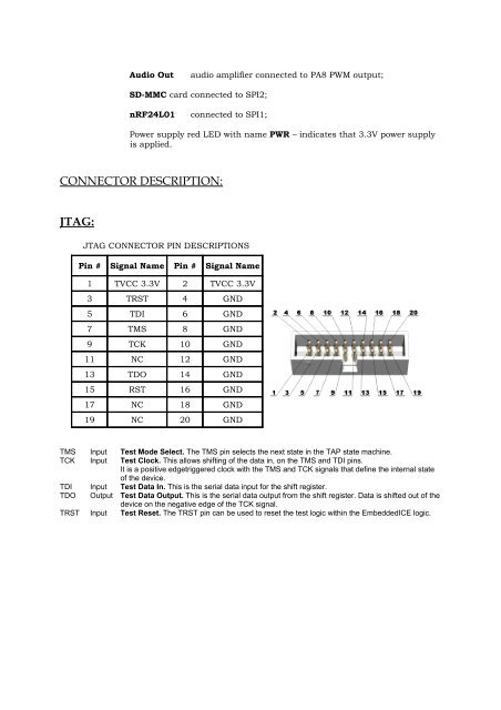
CONNECTOR DESCRIPTION:<br />
JTAG:<br />
JTAG CONNECTOR PIN DESCRIPTIONS<br />
Pin # Signal Name Pin # Signal Name<br />
1 TVCC 3.3V 2 TVCC 3.3V<br />
3 TRST 4 GND<br />
5 TDI 6 GND<br />
7 TMS 8 GND<br />
9 TCK 10 GND<br />
11 NC 12 GND<br />
13 TDO 14 GND<br />
15 RST 16 GND<br />
17 NC 18 GND<br />
19 NC 20 GND<br />
TMS Input Test Mode Select. The TMS pin selects the next state in the TAP state machine.<br />
TCK Input Test Clock. This allows shifting of the data in, on the TMS and TDI pins.<br />
It is a positive edgetriggered clock with the TMS and TCK signals that define the internal state<br />
of the device.<br />
TDI Input Test Data In. This is the serial data input for the shift register.<br />
TDO Output Test Data Output. This is the serial data output from the shift register. Data is shifted out of the<br />
device on the negative edge of the TCK signal.<br />
TRST Input Test Reset. The TRST pin can be used to reset the test logic within the EmbeddedICE logic.