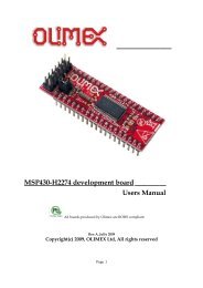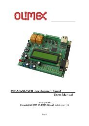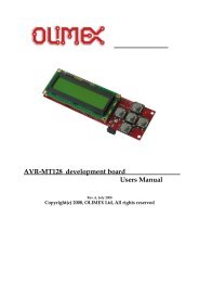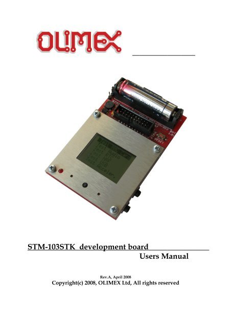
STM-103STK development board Users Manual
STM-103STK development board Users Manual
STM-103STK development board Users Manual

Create successful ePaper yourself
Turn your PDF publications into a flip-book with our unique Google optimized e-Paper software.
<strong>STM</strong>-<strong>103STK</strong> <strong>development</strong> <strong>board</strong><br />
<strong>Users</strong> <strong>Manual</strong><br />
Rev.A, April 2008<br />
Copyright(c) 2008, OLIMEX Ltd, All rights reserved
INTRODUCTION:<br />
BOARD FEATURES:<br />
The ARM Cortex-M3 processor is the latest generation of ARM processors<br />
for embedded systems. It has been developed to provide a low-cost platform<br />
that meets the needs of MCU implementation, with a reduced pin count<br />
and low-power consumption, while delivering outstanding computational<br />
performance and an advanced system response to interrupts. The ARM<br />
Cortex-M3 32-bit RISC processor features exceptional code-efficiency,<br />
delivering the high-performance expected from an ARM core in the memory<br />
size usually associated with 8- and 16-bit devices.<br />
The <strong>STM</strong>32F103 Performance Line family has an embedded ARM core and<br />
is therefore compatible with all ARM tools and software. It combines the<br />
high performance ARM Cortex-M3 CPU with an extensive range of<br />
peripheral functions and enhanced I/O capabilities.<br />
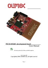
<strong>STM</strong>32-<strong>103STK</strong> is starter-kit <strong>board</strong> which allow you to explore the<br />
complete features of the new ARM Cortex M3 <strong>STM</strong>32F103RBT6<br />
microcontrollers produced by ST Microelectronics Inc. It have NOKIA 3310<br />
BW 84x48 LCD, buttons, SD-MMC card, 3-axis digital accelerometer,<br />
2.4Ghz RF transciever, Audio Input and Output, the power supply is made<br />
from single 1.5V AA cell battery.<br />
Some applications are USB Mass Storage device, Audio class device, HID<br />
mouse device, CDC Virtual com port device, USB Wireless RF link.The UXT<br />
connector allow access to all other UEXT modules produced by OLIMEX<br />
like MOD-MP3, MOD-NRF24LR, MOD-NOKIA6610 etc to be connected<br />
easily. In the prototype area customer can solder his own custom circuits<br />
and to interface them to USB, CAN, RS232 etc.<br />
- MCU: <strong>STM</strong>32F103RBT6 ARM 32 bit CORTEX M3 with 128K Bytes<br />
Program Flash, 20K Bytes RAM, USB, CAN, x2 I2C, x2 ADC 12 bit, x3<br />
UART, x2 SPI, x3 TIMERS, up to 72Mhz operation<br />
- standard JTAG connector with ARM 2x10 pin layout for<br />
programming/debugging with ARM-JTAG<br />
- USB mini connector<br />
- LCD NOKIA 3310 BW 84x48 pixels<br />
- 1.5V battery connector with step-up converter<br />
- 3-axis accelerometer<br />
- SD-MMC card<br />
- 2.4 Ghz transciever with Nordic nRF24L01<br />
- Audio input<br />
- Audio output<br />
- user buttions x2<br />
- Joystick with 4 directions and push action<br />
- UEXT connector for other Olimex's modules connection like MOD-MP3,<br />
etc.<br />
- RESET button<br />
- status LED<br />
- 8 Mhz crystal oscillator<br />
- 32768 Hz crystal and RTC backup battery connector<br />
- extension headers for all uC ports<br />
- PCB: FR-4, 1.5 mm (0,062"), soldermask, silkscreen component print<br />
- Dimensions: 90 x 65mm (3.5 x 2.5")
ELECTROSTATIC WARNING:<br />
The <strong>STM</strong>32-<strong>103STK</strong> <strong>board</strong> is shipped in protective anti-static packaging.<br />
The <strong>board</strong> must not be subject to high electrostatic potentials. General<br />
practice for working with static sensitive devices should be applied when<br />
working with this <strong>board</strong>.<br />
BOARD USE REQUIREMENTS:<br />
Cables: 1.8 meter A-to-miniUSB cable to connect to USB host.<br />
Hardware: ARM-JTAG, ARM-USB-OCD, ARM-USB-TINY or other ARM<br />
JTAG compatible tool<br />
Software: ARM C compiler and debugger software, the possible options<br />
are:<br />
- free open source platform: GNU C compiler + OpenOCD<br />
and Eclipse (support all low cost Olimex JTAG debuggers)<br />
- commercial solution EW-ARM from IAR Systems AB,<br />
require expensive J-LINK debugger<br />
- CrossWorks from Rowley (supports all Olimex low cost<br />
JTAG debuggers).
BOARD LAYOUT:
SCHEMATIC:
PROCESSOR FEATURES:<br />
RS232:<br />
SPI:<br />
I2C:<br />
<strong>STM</strong>-<strong>103STK</strong> <strong>board</strong> use ARM 32-bit Cortex-M3 CPU <strong>STM</strong>32F103RBT6<br />
from ST Microelectronics with these features:<br />
- CPU clock up to 72Mhz<br />
- FLASH 128KB<br />
- RAM 20KB<br />
- DMA x7 channels<br />
- RTC<br />
- WDT<br />
- Timers x3+1<br />
- SPI x2<br />
- I2C x2<br />
- USART x3<br />
- USB x1<br />
- CAN x1 (multiplexed with USB so both can't be used in same time)<br />
- GPIO up to 51 (multiplexed with peripherials)<br />
- 2 ADC 12-bit<br />
- operating voltage 2.0-3.6V<br />
- temperature -40C +85C<br />
<strong>STM</strong>32F103RBT6 have 3 USARTs which are available on the extension<br />
headers. One of them can operate up to 4.5 Mbit/s, the other two up to<br />
2.25 Mbit/s. They provide hardware management of the CTS and RTS<br />
signals, IrDA SIR ENDEC support, are ISO 7816 compliant and have LIN<br />
Master/Slave capability.<br />
All USART interfaces can be served by the DMA controller.<br />
<strong>STM</strong>32F103RBT6 have 2 SPIs which able to communicate up to 18 Mbits/s<br />
in slave and master modes in fullduplex and simplex communication<br />
modes. The 3-bit prescaler gives 8 master mode frequencies and the frame<br />
is configurable from 8-bit to 16-bit. The hardware CRC<br />
generation/verification supports basic SD Card/MMC modes.<br />
Both SPIs can be served by the DMA controller.<br />
<strong>STM</strong>32F103RBT6 have two I²C bus interfaces which can operate in multimaster<br />
and slave modes. They can support<br />
standard and fast modes. They support dual slave addressing (7-bit only)<br />
and both 7/10-bit addressing in master<br />
mode. A hardware CRC generation/verification is embedded.<br />
They can be served by DMA and they support SM Bus 2.0/PM Bus.
CAN:<br />
USB:<br />
ADC:<br />
The <strong>STM</strong>32F103RBT6 CAN is compliant with specifications 2.0A and B<br />
(active) with a bit rate up to 1 Mbit/s. It can receive and transmit standard<br />
frames with 11-bit identifiers as well as extended frames with 29-bit<br />
identifiers. It has three transmit mailboxes, two receive FIFOs with 3 stages<br />
and 14 scalable filter banks.<br />
The CAN and USB share same pins PA11 and PA12, so you can’t use both<br />
CAN and USB on same time.<br />
The <strong>STM</strong>32F103RBT6 embeds a USB device peripheral compatible with the<br />
USB Full-speed 12 Mbs. The USB interface implements a full speed (12<br />
Mbit/s) function interface. It has software configurable endpoint setting<br />
and suspend/resume support. The dedicated 48 MHz clock source is<br />
generated from the internal main PLL.<br />
The CAN and USB share same pins PA11 and PA12, so you can’t use both<br />
CAN and USB on same time.<br />
<strong>STM</strong>32F103RBT6 have two 12-bit Analog to Digital Converters which share<br />
up to 16 external channels, performing conversions in singleshot or scan<br />
modes. In scan mode, automatic conversion is performed on a selected<br />
group of analog inputs.<br />
Additional logic functions embedded in the ADC interface allow:<br />
- Simultaneous sample and hold<br />
- Interleaved sample and hold<br />
- Single shunt<br />
The ADC can be served by the DMA controller.<br />
An analog watchdog feature allows very precise monitoring of the converted<br />
voltage of one, some or all selected channels. An interrupt is generated<br />
when the converted voltage is outside the programmed thresholds. The<br />
events generated by the standard timers (TIMx) and the Advanced Control<br />
timer (TIM1) can be internally connected to the ADC start trigger, injection<br />
trigger, and DMA trigger respectively, to allow the application to<br />
synchronize A/D conversion and timers.
BLOCK DIAGRAM:
MEMORY MAP:
POWER SUPPLY CIRCUIT:<br />
RESET CIRCUIT:<br />
CLOCK CIRCUIT:<br />
<strong>STM</strong>32-<strong>103STK</strong> can take power from these sources:<br />
– 1.5V battery with DC/DC step up converter<br />
– Vin signal on EXT1-11 pin.<br />
- JTAG pin.1 or 2<br />
The <strong>board</strong> power consumption is: about 30 mA when powered from the<br />
USB port and 130mA when powered from 1.5V battery with all peripherials<br />
and MCU running at full speed, there are different power saving modes<br />
which may put <strong>STM</strong>32F103RBT6 in power sleep mode and in these modes<br />
the consumption of the MCU is only few microampers.<br />
<strong>STM</strong>32-<strong>103STK</strong> reset circuit is made with RC group R8 - 10K and C28-<br />
100nF.<br />
Although on the schematic is made provision for external reset IC such is<br />
not necessary as <strong>STM</strong>32 have build-in brown out detector. <strong>Manual</strong> reset is<br />
possible by the RESET button.<br />
Quartz crystal 8Mhz is connected to <strong>STM</strong>32F103RBT6. Internal PLL circuit<br />
can multiply this frequency up to 72Mhz.<br />
32.768 KHz quartz crystal is connected to <strong>STM</strong>32F103RBT6 for it’s internal<br />
Real Time Clock.<br />
JUMPER DESCRIPTION:<br />
EXT/BAT 3 pin, power supply select jumper.<br />
EXT position EXT/BAT<br />
Allow power supply from mini-USB connector or EXT1(pin11).<br />
The voltage supplied to EXT1(pin 11) must be between 5VDC<br />
and 9VDC.<br />
BAT position EXT/BAT<br />
Allow power supply from 1.5V AA (R6), no charge battery,<br />
pluged in the BAT connector.<br />
R-T Connects JTAG TRST signal to <strong>STM</strong>32F103RBT6 RESET<br />
Default state closed (shorted)<br />
BAT_E Connects 3.3V to <strong>STM</strong>32F103RBT6 Vbat pin.1<br />
Default state closed (shorten), Vbat signal is also available to<br />
EXT1 (pin 1) connector, so if you want to connect external<br />
backup battery to the <strong>STM</strong>32F103RBT6 this jumper should be<br />
opened (unshorted) and the external battery to be connected to<br />
EXT1 (pin 1) connector(see connector description for EXT1<br />
connector pining.).VBAT accept 2 - 3.6V.
INPUT/OUTPUT:<br />
USBP-E Connects USB power supply to <strong>STM</strong>32F103RBT6 pin 24 PC4/<br />
ADC14 and allow to detect if the <strong>board</strong> is connected to USB<br />
host.<br />
Default state closed (shorten)<br />
LED-E Connects STATUS LED to <strong>STM</strong>32F103RBT6 pin 53 PC12<br />
Default state closed (shorten)<br />
BOOT0, BOOT1 boot sequence select<br />
B1_H/B1_L (Boot1_High/Boot1_Low)<br />
B0_L/B0_H (Boot0_Low /Boot0_ High)<br />
B1_H/B1_L<br />
Default position: Boot1 is log. 0<br />
Boot0 is log. 0<br />
B0_L/B0_H<br />
CP_E Card Present Enable – Allow PC1(pin 9) to detect Multi Media<br />
Card present in socket. Log. 1 of PC1 – MMC present. Log.0 of<br />
PC1 – Card absent.<br />
Default state closed (shorten)<br />
WP_E Write Protect Enable – Allow PC2(pin 10) to detect write<br />
protected state of Multi Media Card. Log. 1 of PC2 – MMC no<br />
write protected . Log.0 of PC2 – MMC is write protected.<br />
Default state closed (shorten)<br />
3.3V_E Connect 3.3V regulated voltage to <strong>STM</strong>32F103RBT6 power<br />
pins. 3.3V_E jumper is used if you need to measure current<br />
consumption of the microcontroller.<br />
Default state closed (shorten)<br />
JOYSTICK this is 4 directions plus center button, in the schematic the<br />
joystick four directions switches are connected through resistors with<br />
different values to PC5/ADC15 , the center button is connected to PC6;<br />
BUTTON B1 Left button connected to PC13/TAMPER port;<br />
BUTTON B2 Right button connected to PA0/WAKE-UP port;<br />
LCD NOKIA3310 84x48 pixel black and white LCD to SPI1 port;<br />
ACCELEROMETER 3-axis accelerometer connected to I2C1 port;<br />
Audio In microphone with pre-amplifier connected to PA1 ADC;
Audio Out audio amplifier connected to PA8 PWM output;<br />
SD-MMC card connected to SPI2;<br />
nRF24L01 connected to SPI1;<br />
Power supply red LED with name PWR – indicates that 3.3V power supply<br />
is applied.<br />
CONNECTOR DESCRIPTION:<br />
JTAG:<br />
JTAG CONNECTOR PIN DESCRIPTIONS<br />
Pin # Signal Name Pin # Signal Name<br />
1 TVCC 3.3V 2 TVCC 3.3V<br />
3 TRST 4 GND<br />
5 TDI 6 GND<br />
7 TMS 8 GND<br />
9 TCK 10 GND<br />
11 NC 12 GND<br />
13 TDO 14 GND<br />
15 RST 16 GND<br />
17 NC 18 GND<br />
19 NC 20 GND<br />
TMS Input Test Mode Select. The TMS pin selects the next state in the TAP state machine.<br />
TCK Input Test Clock. This allows shifting of the data in, on the TMS and TDI pins.<br />
It is a positive edgetriggered clock with the TMS and TCK signals that define the internal state<br />
of the device.<br />
TDI Input Test Data In. This is the serial data input for the shift register.<br />
TDO Output Test Data Output. This is the serial data output from the shift register. Data is shifted out of the<br />
device on the negative edge of the TCK signal.<br />
TRST Input Test Reset. The TRST pin can be used to reset the test logic within the EmbeddedICE logic.
EXT1<br />
Pin # Signal Name Pin # Signal Name<br />
1 VBAT 2<br />
3<br />
PA9/USART1_TX/<br />
TIM1_CH2<br />
4<br />
PA3/USART2_RX/<br />
ADC3/TIM2_CH4<br />
PA10/USART1_RX/<br />
TIM1_CH2<br />
5 RD0/OSC_IN 6 PC12/LED<br />
7<br />
9<br />
PC4/ADC14/<br />
USB_PRESENT<br />
PA2/USART2_TX/<br />
ADC2/ITIM2_CH3<br />
8<br />
PC3/ADC13/<br />
STNBY<br />
10 NRST<br />
11 VIN 12 +5.0V<br />
13 3.3V 14 GND<br />
EXT2<br />
Pin # Signal Name Pin # Signal Name<br />
1 PB0/ADC8/TIM3_CH3 2 PB1/ADC9/TIM3_CH4<br />
3 PB8/TIM4_CH3 4 PB9/TIM4_CH4<br />
5 SCL2 6 SDA2<br />
7 PC0/ADC10 8 CP<br />
9 WP 10 3.3V_A<br />
11 AGND 12 +5.0<br />
13 3.3V 14 GND<br />
UEXT<br />
Pin # Signal Name Pin # Signal Name<br />
1 VCC 3.3V 2 GND<br />
3 TX2 4 RX2<br />
5 SCL2 6 SDA2<br />
7 SPI2_MISO 8 SPI2_MOSI<br />
9 SPI2_SCK 10 SPI2_NSS
SD-MMC<br />
USB<br />
Pin # Signal Name Pin # Signal Name<br />
1 SPI2_NSS 2 SPI2_MOSI<br />
3 GND 4 VCC<br />
5 SPI2_SCK 6 GND<br />
7 SPI2_MISO 8 10K to 3.3V<br />
9 10K to 3.3V 10 WP_E<br />
11 to pin 14 12 to pin 15<br />
13 CP_E 14 2K to 3.3V<br />
15 2K to 3.3V<br />
Pin # Signal Name<br />
1 VBUS<br />
2 USBDM<br />
3 USBDP<br />
4 NC<br />
5 GND<br />
AVAILABLE DEMO SOFTWARE:<br />
– USB mouse with the 3-axis accelerometer<br />
– USB class Audio device<br />
– USB mass storage<br />
– USB Virtual com port<br />
– USB RF Virtual com port bridge<br />
– Ball game with accelerometer<br />
– OpenOCD demo project
ORDER CODE:<br />
Revision history:<br />
REV.A - create April 2008<br />
<strong>STM</strong>32-<strong>103STK</strong> – assembled and tested (no kit, no soldering required)<br />
How to order?<br />
You can order to us directly or by any of our distributors.<br />
Check our web www.olimex.com/dev for more info.<br />
All <strong>board</strong>s produced by Olimex are ROHS compliant
Disclaimer:<br />
© 2008 Olimex Ltd. All rights reserved. Olimex®, logo and combinations thereof, are registered trademarks of<br />
Olimex Ltd. Other terms and product names may be trademarks of others.<br />
The information in this document is provided in connection with Olimex products. No license, express or implied<br />
or otherwise, to any intellectual property right is granted by this document or in connection with the sale of Olimex<br />
products.<br />
Neither the whole nor any part of the information contained in or the product described in this document may be<br />
adapted or reproduced in any material from except with the prior written permission of the copyright holder.<br />
The product described in this document is subject to continuous <strong>development</strong> and improvements. All particulars of<br />
the product and its use contained in this document are given by OLIMEX in good faith. However all warranties<br />
implied or expressed including but not limited to implied warranties of merchantability or fitness for purpose are<br />
excluded.<br />
This document is intended only to assist the reader in the use of the product. OLIMEX Ltd. shall not be liable for<br />
any loss or damage arising from the use of any information in this document or any error or omission in such<br />
information or any incorrect use of the product.