TL494 pwm smps kontrol - 320Volt
TL494 pwm smps kontrol - 320Volt
TL494 pwm smps kontrol - 320Volt
- No tags were found...

You also want an ePaper? Increase the reach of your titles
YUMPU automatically turns print PDFs into web optimized ePapers that Google loves.
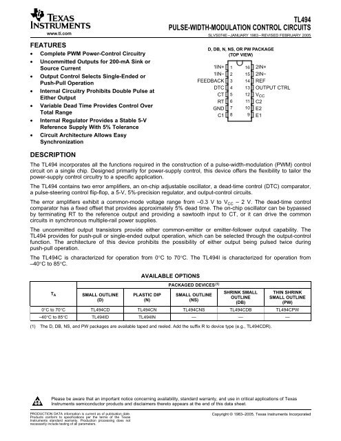
www.ti.comFEATURES• Complete PWM Power-Control Circuitry• Uncommitted Outputs for 200-mA Sink orSource Current• Output Control Selects Single-Ended orPush-Pull Operation• Internal Circuitry Prohibits Double Pulse atEither Output• Variable Dead Time Provides Control OverTotal Range• Internal Regulator Provides a Stable 5-VReference Supply With 5% Tolerance• Circuit Architecture Allows EasySynchronization<strong>TL494</strong>PULSE-WIDTH-MODULATION CONTROL CIRCUITSSLVS074E–JANUARY 1983–REVISED FEBRUARY 2005D, DB, N, NS, OR PW PACKAGE(TOP VIEW)1IN+1IN−FEEDBACKDTCCTRTGNDC1123456781615141312111092IN+2IN−REFOUTPUT CTRLV CCC2E2E1DESCRIPTIONThe <strong>TL494</strong> incorporates all the functions required in the construction of a pulse-width-modulation (PWM) controlcircuit on a single chip. Designed primarily for power-supply control, this device offers the flexibility to tailor thepower-supply control circuitry to a specific application.The <strong>TL494</strong> contains two error amplifiers, an on-chip adjustable oscillator, a dead-time control (DTC) comparator,a pulse-steering control flip-flop, a 5-V, 5%-precision regulator, and output-control circuits.The error amplifiers exhibit a common-mode voltage range from –0.3 V to V CC – 2 V. The dead-time controlcomparator has a fixed offset that provides approximately 5% dead time. The on-chip oscillator can be bypassedby terminating RT to the reference output and providing a sawtooth input to CT, or it can drive the commoncircuits in synchronous multiple-rail power supplies.The uncommitted output transistors provide either common-emitter or emitter-follower output capability. The<strong>TL494</strong> provides for push-pull or single-ended output operation, which can be selected through the output-controlfunction. The architecture of this device prohibits the possibility of either output being pulsed twice duringpush-pull operation.The <strong>TL494</strong>C is characterized for operation from 0°C to 70°C. The <strong>TL494</strong>I is characterized for operation from–40°C to 85°C.AVAILABLE OPTIONSPACKAGED DEVICES (1)T SHRINK SMALL THIN SHRINKA SMALL OUTLINE PLASTIC DIP SMALL OUTLINEOUTLINE SMALL OUTLINE(D) (N) (NS)(DB)(PW)0°C to 70°C <strong>TL494</strong>CD <strong>TL494</strong>CN <strong>TL494</strong>CNS <strong>TL494</strong>CDB <strong>TL494</strong>CPW–40°C to 85°C <strong>TL494</strong>ID <strong>TL494</strong>IN — — —(1) The D, DB, NS, and PW packages are available taped and reeled. Add the suffix R to device type (e.g., <strong>TL494</strong>CDR).Please be aware that an important notice concerning availability, standard warranty, and use in critical applications of TexasInstruments semiconductor products and disclaimers thereto appears at the end of this data sheet.PRODUCTION DATA information is current as of publication date.Products conform to specifications per the terms of the TexasInstruments standard warranty. Production processing does notnecessarily include testing of all parameters.Copyright © 1983–2005, Texas Instruments Incorporated
<strong>TL494</strong>PULSE-WIDTH-MODULATION CONTROL CIRCUITSSLVS074E–JANUARY 1983–REVISED FEBRUARY 2005www.ti.comFUNCTION TABLEINPUT TOOUTPUT CTRLV I = GNDV I = V refOUTPUT FUNCTIONSingle-ended or parallel outputNormal push-pull operationFUNCTIONAL BLOCK DIAGRAMOUTPUT CTRL(see Function Table)RTCTDTC654≈0.1 VOscillatorDead-Time ControlComparator1DC113Q189C1E11IN+1IN−12≈0.7 VError Amplifier 1+−PWMComparatorPulse-SteeringFlip-FlopQ21110C2E22IN+2IN−1615Error Amplifier 2+−ReferenceRegulator1214V CCREF7GNDFEEDBACK30.7 mA2
www.ti.com<strong>TL494</strong>PULSE-WIDTH-MODULATION CONTROL CIRCUITSSLVS074E–JANUARY 1983–REVISED FEBRUARY 2005Absolute Maximum Ratings (1)over operating free-air temperature range (unless otherwise noted)Recommended Operating ConditionsMIN MAX UNITV CC Supply voltage (2) 41 VV I Amplifier input voltage V CC + 0.3 VV O Collector output voltage 41 VI O Collector output current 250 mAD package 73DB package 82θ JA Package thermal impedance (3)(4) N package 67 °C/WNS package 64PW package 108Lead temperature 1,6 mm (1/16 inch) from case for 10 seconds 260 °CT stg Storage temperature range –65 150 °C(1) Stresses beyond those listed under "absolute maximum ratings" may cause permanent damage to the device. These are stress ratingsonly, and functional operation of the device at these or any other conditions beyond those indicated under "recommended operatingconditions" is not implied. Exposure to absolute-maximum-rated conditions for extended periods may affect device reliability.(2) All voltages are with respect to the network ground terminal.(3) Maximum power disipation is a function of T J (max), θ JA , and T A . The maximum allowable power dissipation at any allowable ambienttemperatire is P D = (T J (max) – T A )/θ JA . Operating at the absolute maximum T J of 150°C can affect reliability.(4) The package thermal impedance is calculated in accordance with JESD 51-7.MIN MAX UNITV CC Supply voltage 7 40 VV I Amplifier input voltage –0.3 V CC – 2 VV O Collector output voltage 40 VCollector output current (each transistor) 200 mACurrent into feedback terminal 0.3 mAf OSC Oscillator frequency 1 300 kHzC T Timing capacitor 0.47 10000 nFR T Timing resistor 1.8 500 kΩ<strong>TL494</strong>C 0 70T A Operating free-air temperature °C<strong>TL494</strong>I –40 853
<strong>TL494</strong>PULSE-WIDTH-MODULATION CONTROL CIRCUITSSLVS074E–JANUARY 1983–REVISED FEBRUARY 2005Electrical Characteristicsover recommended operating free-air temperature range, V CC = 15 V, f = 10 kHz (unless otherwise noted)Reference SectionOscillator SectionC T = 0.01 µF, R T = 12 kΩ (see Figure 1) N(x n X) 2n1N 1Error-Amplifier SectionSee Figure 2www.ti.com<strong>TL494</strong>C, <strong>TL494</strong>IPARAMETER TEST CONDITIONS (1) UNITMIN TYP (2) MAXOutput voltage (REF) I O = 1 mA 4.75 5 5.25 VInput regulation V CC = 7 V to 40 V 2 25 mVOutput regulation I O = 1 mA to 10 mA 1 15 mVOutput voltage change with temperature ∆T A = MIN to MAX 2 10 mV/VShort-circuit output current (3) REF = 0 V 25 mA(1) For conditions shown as MIN or MAX, use the appropriate value specified under recommended operating conditions.(2) All typical values, except for parameter changes with temperature, are at T A = 25°C.(3) Duration of short circuit should not exceed one second.<strong>TL494</strong>C, <strong>TL494</strong>IPARAMETER TEST CONDITIONS (1) UNITMIN TYP (2) MAXFrequency 10 kHzStandard deviation of frequency (3) All values of V CC , C T , R T , and T A constant 100 Hz/kHzFrequency change with voltage V CC = 7 V to 40 V, T A = 25°C 1 Hz/kHzFrequency change with temperature (4) ∆T A = MIN to MAX 10 Hz/kHz(1) For conditions shown as MIN or MAX, use the appropriate value specified under recommended operating conditions.(2) All typical values, except for parameter changes with temperature, are at T A = 25°C.(3) Standard deviation is a measure of the statistical distribution about the mean as derived from the formula:(4) Temperature coefficient of timing capacitor and timing resistor are not taken into account.<strong>TL494</strong>C, <strong>TL494</strong>IPARAMETER TEST CONDITIONS UNITMIN TYP (1) MAXInput offset voltage V O (FEEDBACK) = 2.5 V 2 10 mVInput offset current V O (FEEDBACK) = 2.5 V 25 250 nAInput bias current V O (FEEDBACK) = 2.5 V 0.2 1 µA–0.3 toCommon-mode input voltage range V CC = 7 V to 40 V VV CC – 2Open-loop voltage amplification ∆V O = 3 V, V O = 0.5 V to 3.5 V, R L = 2 kΩ 70 95 dBUnity-gain bandwidth V O = 0.5 V to 3.5 V, R L = 2 kΩ 800 kHzCommon-mode rejection ratio ∆V O = 40 V, T A = 25°C 65 80 dBOutput sink current (FEEDBACK) V ID = –15 mV to –5 V, V (FEEDBACK) = 0.7 V 0.3 0.7 mAOutput source current (FEEDBACK) V ID = 15 mV to 5 V, V (FEEDBACK) = 3.5 V –2 mA(1) All typical values, except for parameter changes with temperature, are at T A = 25°C.4
www.ti.com<strong>TL494</strong>PULSE-WIDTH-MODULATION CONTROL CIRCUITSSLVS074E–JANUARY 1983–REVISED FEBRUARY 2005Electrical Characteristicsover recommended operating free-air temperature range, V CC = 15 V, f = 10 kHz (unless otherwise noted)Output SectionDead-Time Control SectionSee Figure 1PWM Comparator SectionSee Figure 1Total DeviceSwitching CharacteristicsT A= 25°CPARAMETER TEST CONDITIONS MIN TYP (1) MAX UNITCollector off-state current V CE = 40 V, V CC = 40 V 2 100 µAEmitter off-state current V CC = V C = 40 V, V E = 0 –100 µACollector-emitter saturation voltageCommon emitter V E = 0, I C = 200 mA 1.1 1.3Emitter follower V O(C1 or C2) = 15 V, I E = –200 mA 1.5 2.5Output control input current V I = V ref 3.5 mA(1) All typical values, except for temperature coefficient, are at T A = 25°C.PARAMETER TEST CONDITIONS MIN TYP (1) MAX UNITInput bias current (DEAD-TIME CTRL) V I = 0 to 5.25 V –2 –10 µAV I (DEAD-TIME CTRL) = 0, C T = 0.01 µF,Maximum duty cycle, each output 45 %R T = 12 kΩInput threshold voltage (DEAD-TIME CTRL)(1) All typical values, except for temperature coefficient, are at T A = 25°C.Zero duty cycle 3 3.3Maximum duty cycle 0PARAMETER TEST CONDITIONS MIN TYP (1) MAX UNITInput threshold voltage (FEEDBACK) Zero duty cyle 4 4.5 VInput sink current (FEEDBACK) V (FEEDBACK) = 0.7 V 0.3 0.7 mA(1) All typical values, except for temperature coefficient, are at T A = 25°C.PARAMETER TEST CONDITIONS MIN TYP (1) MAX UNITStandby supply currentR T = V ref ,V CC = 15 V 6 10All other inputs and outputs open V CC = 40 V 9 15Average supply current V I (DEAD-TIME CTRL) = 2 V, See Figure 1 7.5 mA(1) All typical values, except for temperature coefficient, are at T A = 25°C.PARAMETER TEST CONDITIONS MIN TYP (1) MAX UNITRise time 100 200 nsCommon-emitter configuration, See Figure 3Fall time 25 100 nsRise time 100 200 nsEmitter-follower configuration, See Figure 4Fall time 40 100 nsVVmA(1) All typical values, except for temperature coefficient, are at T A = 25°C.5
<strong>TL494</strong>PULSE-WIDTH-MODULATION CONTROL CIRCUITSSLVS074E–JANUARY 1983–REVISED FEBRUARY 2005www.ti.comPARAMETER MEASUREMENT INFORMATIONV CC = 15 VTestInputs50 kΩ4312 kΩ650.01 µF12161513DTCFEEDBACKRTCT1IN+1IN−2IN+2IN−OUTPUTCTRLV CCGND12ErrorAmplifiers78C1 Output 1E1C2E2REF9111014150 Ω2 W150 Ω2 WOutput 2TEST CIRCUITVoltageat C1Voltageat C2V CC0 VV CC0 VVoltageat CTDTCThreshold Voltage0 VFEEDBACK0.7 VDuty Cycle0%Threshold VoltageMAX 0%VOLTAGE WAVEFORMSFigure 1. Operational Test Circuit and Waveforms6
www.ti.com<strong>TL494</strong>PULSE-WIDTH-MODULATION CONTROL CIRCUITSPARAMETER MEASUREMENT INFORMATIONSLVS074E–JANUARY 1983–REVISED FEBRUARY 2005Amplifier Under Test+V I FEEDBACK−V ref+−Other AmplifierFigure 2. Amplifier Characteristics15 VEach OutputCircuit68 Ω2 WOutputC L = 15 pF(See Note A)90%10%t f10%tr90%NOTE A:TEST CIRCUITC L includes probe and jig capacitance.OUTPUT VOLTAGE WAVEFORMFigure 3. Common-Emitter Configuration15 VEach OutputCircuitC L = 15 pF(See Note A)68 Ω2 WOutput10%90%90%10%t rt fNOTE A:TEST CIRCUITC L includes probe and jig capacitance.OUTPUT VOLTAGE WAVEFORMFigure 4. Emitter-Follower Configuration7
<strong>TL494</strong>PULSE-WIDTH-MODULATION CONTROL CIRCUITSSLVS074E–JANUARY 1983–REVISED FEBRUARY 2005TYPICAL CHARACTERISTICSwww.ti.comf − Oscillator Frequency and Frequency Variation − Hz100 k40 k10 k4 k1 k40010040OSCILLATOR FREQUENCY ANDFREQUENCY VARIATION †vsTIMING RESISTANCE−2%−1%C T = 1 µF0%0.1 µF0.01 µF†Df = 1%101 k 4 k 10 k 40 k 100 k 400 k 1 MR T − Timing Resistance − ΩV CC = 15 VT A = 25°C0.001 µF† Frequency variation (∆f) is the change in oscillator frequency that occurs over the full temperature range.Figure 5.A − Amplifier Voltage Amplification − dB100908070605040302010AMPLIFIER VOLTAGE AMPLIFICATIONvsFREQUENCYV CC = 15 V∆V O = 3 VT A = 25°C01 10 100 1 k 10 k 100 k 1 Mf − Frequency − HzFigure 6.8
Application ReportSLVA001D - December 2003 − Revised February 2005Designing Switching Voltage Regulators With the <strong>TL494</strong>Patrick GriffithStandard Linear & LogicABSTRACTThe <strong>TL494</strong> power-supply controller is discussed in detail. A general overview of the <strong>TL494</strong>architecture presents the primary functional blocks contained in the device. An in-depth studyof the interrelationship between the functional blocks highlights versatility and limitations ofthe <strong>TL494</strong>. The usefulness of the <strong>TL494</strong> power-supply controller also is demonstratedthrough several basic applications, and a design example is included for a 5-V/10-A powersupply.ContentsIntroduction . . . . . . . . . . . . . . . . . . . . . . . . . . . . . . . . . . . . . . . . . . . . . . . . . . . . . . . . . . . . . . . . . . . . . . . . . . . . . 4The Basic Device . . . . . . . . . . . . . . . . . . . . . . . . . . . . . . . . . . . . . . . . . . . . . . . . . . . . . . . . . . . . . . . . . . . . . . . . . 4Principle of Operation . . . . . . . . . . . . . . . . . . . . . . . . . . . . . . . . . . . . . . . . . . . . . . . . . . . . . . . . . . . . . . . . . . . . 55-V Reference Regulator . . . . . . . . . . . . . . . . . . . . . . . . . . . . . . . . . . . . . . . . . . . . . . . . . . . . . . . . . . . . . . 5Oscillator . . . . . . . . . . . . . . . . . . . . . . . . . . . . . . . . . . . . . . . . . . . . . . . . . . . . . . . . . . . . . . . . . . . . . . . . . . . . 7Operation Frequency . . . . . . . . . . . . . . . . . . . . . . . . . . . . . . . . . . . . . . . . . . . . . . . . . . . . . . . . . . . . . 7Operation Above 150 kHz . . . . . . . . . . . . . . . . . . . . . . . . . . . . . . . . . . . . . . . . . . . . . . . . . . . . . . . . . 8Dead-Time Control/PWM Comparator . . . . . . . . . . . . . . . . . . . . . . . . . . . . . . . . . . . . . . . . . . . . . . . . . . . 9Dead-Time Control . . . . . . . . . . . . . . . . . . . . . . . . . . . . . . . . . . . . . . . . . . . . . . . . . . . . . . . . . . . . . . . 9Comparator . . . . . . . . . . . . . . . . . . . . . . . . . . . . . . . . . . . . . . . . . . . . . . . . . . . . . . . . . . . . . . . . . . . . . 10Pulse-Width Modulation (PWM) . . . . . . . . . . . . . . . . . . . . . . . . . . . . . . . . . . . . . . . . . . . . . . . . . . . 10Error Amplifiers . . . . . . . . . . . . . . . . . . . . . . . . . . . . . . . . . . . . . . . . . . . . . . . . . . . . . . . . . . . . . . . . . 10Output-Control Logic . . . . . . . . . . . . . . . . . . . . . . . . . . . . . . . . . . . . . . . . . . . . . . . . . . . . . . . . . . . . . . . . . 13Output-Control Input . . . . . . . . . . . . . . . . . . . . . . . . . . . . . . . . . . . . . . . . . . . . . . . . . . . . . . . . . . . . . 13Pulse-Steering Flip-Flop . . . . . . . . . . . . . . . . . . . . . . . . . . . . . . . . . . . . . . . . . . . . . . . . . . . . . . . . . . 15Output Transistors . . . . . . . . . . . . . . . . . . . . . . . . . . . . . . . . . . . . . . . . . . . . . . . . . . . . . . . . . . . . . . . . . . . 15Applications . . . . . . . . . . . . . . . . . . . . . . . . . . . . . . . . . . . . . . . . . . . . . . . . . . . . . . . . . . . . . . . . . . . . . . . . . . . . 17Reference Regulator . . . . . . . . . . . . . . . . . . . . . . . . . . . . . . . . . . . . . . . . . . . . . . . . . . . . . . . . . . . . . . . . . 17Current Boosting the 5-V Regulator . . . . . . . . . . . . . . . . . . . . . . . . . . . . . . . . . . . . . . . . . . . . . . . . 17Applications of the Oscillator . . . . . . . . . . . . . . . . . . . . . . . . . . . . . . . . . . . . . . . . . . . . . . . . . . . . . . . . . . 18Synchronization . . . . . . . . . . . . . . . . . . . . . . . . . . . . . . . . . . . . . . . . . . . . . . . . . . . . . . . . . . . . . . . . . 18Master/Slave Synchronization . . . . . . . . . . . . . . . . . . . . . . . . . . . . . . . . . . . . . . . . . . . . . . . . . . . . . 18Master Clock Operation . . . . . . . . . . . . . . . . . . . . . . . . . . . . . . . . . . . . . . . . . . . . . . . . . . . . . . . . . . 18Fail-Safe Operation . . . . . . . . . . . . . . . . . . . . . . . . . . . . . . . . . . . . . . . . . . . . . . . . . . . . . . . . . . . . . . 19Error-Amplifier-Bias Configuration . . . . . . . . . . . . . . . . . . . . . . . . . . . . . . . . . . . . . . . . . . . . . . . . . . . . . . 20Current Limiting . . . . . . . . . . . . . . . . . . . . . . . . . . . . . . . . . . . . . . . . . . . . . . . . . . . . . . . . . . . . . . . . . . . . . . 20Fold-Back Current Limiting . . . . . . . . . . . . . . . . . . . . . . . . . . . . . . . . . . . . . . . . . . . . . . . . . . . . . . . . 20Pulse-Current Limiting . . . . . . . . . . . . . . . . . . . . . . . . . . . . . . . . . . . . . . . . . . . . . . . . . . . . . . . . . . . 21Trademarks are the property of their respective owners.1
SLVA001DApplications of the Dead-Time Control . . . . . . . . . . . . . . . . . . . . . . . . . . . . . . . . . . . . . . . . . . . . . . . . . . 23Soft Start . . . . . . . . . . . . . . . . . . . . . . . . . . . . . . . . . . . . . . . . . . . . . . . . . . . . . . . . . . . . . . . . . . . . . . . 23Overvoltage Protection . . . . . . . . . . . . . . . . . . . . . . . . . . . . . . . . . . . . . . . . . . . . . . . . . . . . . . . . . . . 24Modulation of Turnon/Turnoff Transition . . . . . . . . . . . . . . . . . . . . . . . . . . . . . . . . . . . . . . . . . . . . 24Design Example . . . . . . . . . . . . . . . . . . . . . . . . . . . . . . . . . . . . . . . . . . . . . . . . . . . . . . . . . . . . . . . . . . . . . . . . . 25Input Power Source . . . . . . . . . . . . . . . . . . . . . . . . . . . . . . . . . . . . . . . . . . . . . . . . . . . . . . . . . . . . . . . . . . 26Control Circuits . . . . . . . . . . . . . . . . . . . . . . . . . . . . . . . . . . . . . . . . . . . . . . . . . . . . . . . . . . . . . . . . . . . . . . 27Oscillator . . . . . . . . . . . . . . . . . . . . . . . . . . . . . . . . . . . . . . . . . . . . . . . . . . . . . . . . . . . . . . . . . . . . . . . 27Error Amplifier . . . . . . . . . . . . . . . . . . . . . . . . . . . . . . . . . . . . . . . . . . . . . . . . . . . . . . . . . . . . . . . . . . 28Current-Limiting Amplifier . . . . . . . . . . . . . . . . . . . . . . . . . . . . . . . . . . . . . . . . . . . . . . . . . . . . . . . . . 28Soft Start and Dead Time . . . . . . . . . . . . . . . . . . . . . . . . . . . . . . . . . . . . . . . . . . . . . . . . . . . . . . . . . 29Inductor Calculations . . . . . . . . . . . . . . . . . . . . . . . . . . . . . . . . . . . . . . . . . . . . . . . . . . . . . . . . . . . . . . . . . 30Output Capacitance Calculations . . . . . . . . . . . . . . . . . . . . . . . . . . . . . . . . . . . . . . . . . . . . . . . . . . . . . . 30Transistor Power-Switch Calculations . . . . . . . . . . . . . . . . . . . . . . . . . . . . . . . . . . . . . . . . . . . . . . . . . . . 31List of Figures1. <strong>TL494</strong> Block Diagram . . . . . . . . . . . . . . . . . . . . . . . . . . . . . . . . . . . . . . . . . . . . . . . . . . . . . . . . . . . . . . . . . . 42. <strong>TL494</strong> Modulation Technique . . . . . . . . . . . . . . . . . . . . . . . . . . . . . . . . . . . . . . . . . . . . . . . . . . . . . . . . . . . 53. 5-V Reference Regulator . . . . . . . . . . . . . . . . . . . . . . . . . . . . . . . . . . . . . . . . . . . . . . . . . . . . . . . . . . . . . . . 64. Reference Voltage vs Input Voltage . . . . . . . . . . . . . . . . . . . . . . . . . . . . . . . . . . . . . . . . . . . . . . . . . . . . . . 65. Internal-Oscillator Schematic . . . . . . . . . . . . . . . . . . . . . . . . . . . . . . . . . . . . . . . . . . . . . . . . . . . . . . . . . . . . 76. Oscillator Frequency vs R T /C T . . . . . . . . . . . . . . . . . . . . . . . . . . . . . . . . . . . . . . . . . . . . . . . . . . . . . . . . . . 87. Variation of Dead Time vs R T /C T . . . . . . . . . . . . . . . . . . . . . . . . . . . . . . . . . . . . . . . . . . . . . . . . . . . . . . . . 88. Dead-Time Control/PWM Comparator . . . . . . . . . . . . . . . . . . . . . . . . . . . . . . . . . . . . . . . . . . . . . . . . . . . . 99. Error Amplifiers . . . . . . . . . . . . . . . . . . . . . . . . . . . . . . . . . . . . . . . . . . . . . . . . . . . . . . . . . . . . . . . . . . . . . . 1110. Multiplex Structure of Error Amplifiers . . . . . . . . . . . . . . . . . . . . . . . . . . . . . . . . . . . . . . . . . . . . . . . . . . . 1111. Error-Amplifier-Bias Configurations for Controlled-Gain Applications . . . . . . . . . . . . . . . . . . . . . . . . 1212. Amplifier Transfer Characteristics . . . . . . . . . . . . . . . . . . . . . . . . . . . . . . . . . . . . . . . . . . . . . . . . . . . . . . . 1213. Amplifier Bode Plot . . . . . . . . . . . . . . . . . . . . . . . . . . . . . . . . . . . . . . . . . . . . . . . . . . . . . . . . . . . . . . . . . . . 1214. Output-Steering Architecture . . . . . . . . . . . . . . . . . . . . . . . . . . . . . . . . . . . . . . . . . . . . . . . . . . . . . . . . . . . 1415. Pulse-Steering Flip-Flop . . . . . . . . . . . . . . . . . . . . . . . . . . . . . . . . . . . . . . . . . . . . . . . . . . . . . . . . . . . . . . . 1516. Output-Transistor Structure . . . . . . . . . . . . . . . . . . . . . . . . . . . . . . . . . . . . . . . . . . . . . . . . . . . . . . . . . . . . 1617. Conventional Three-Terminal Regulator Current-Boost Technique . . . . . . . . . . . . . . . . . . . . . . . . . . 1718. <strong>TL494</strong> Reference Regulator Current-Boost Technique . . . . . . . . . . . . . . . . . . . . . . . . . . . . . . . . . . . . . 1719. Master/Slave Synchronization . . . . . . . . . . . . . . . . . . . . . . . . . . . . . . . . . . . . . . . . . . . . . . . . . . . . . . . . . . 1820. External Clock Synchronization . . . . . . . . . . . . . . . . . . . . . . . . . . . . . . . . . . . . . . . . . . . . . . . . . . . . . . . . 1921. Oscillator Start-Up Circuit . . . . . . . . . . . . . . . . . . . . . . . . . . . . . . . . . . . . . . . . . . . . . . . . . . . . . . . . . . . . . . 1922. Fail-Safe Protection . . . . . . . . . . . . . . . . . . . . . . . . . . . . . . . . . . . . . . . . . . . . . . . . . . . . . . . . . . . . . . . . . . . 1923. Error-Amplifier-Bias Configurations . . . . . . . . . . . . . . . . . . . . . . . . . . . . . . . . . . . . . . . . . . . . . . . . . . . . . 2024. Fold-Back Current Limiting . . . . . . . . . . . . . . . . . . . . . . . . . . . . . . . . . . . . . . . . . . . . . . . . . . . . . . . . . . . . 2025. Fold-Back Current Characteristics . . . . . . . . . . . . . . . . . . . . . . . . . . . . . . . . . . . . . . . . . . . . . . . . . . . . . . 2126. Error-Signal Considerations . . . . . . . . . . . . . . . . . . . . . . . . . . . . . . . . . . . . . . . . . . . . . . . . . . . . . . . . . . . 222 Designing Switching Voltage Regulators With the <strong>TL494</strong>
SLVA001D27. Peak-Current Protection . . . . . . . . . . . . . . . . . . . . . . . . . . . . . . . . . . . . . . . . . . . . . . . . . . . . . . . . . . . . . . . 2228. Dead-Time Control Characteristics . . . . . . . . . . . . . . . . . . . . . . . . . . . . . . . . . . . . . . . . . . . . . . . . . . . . . 2329. Tailored Dead Time . . . . . . . . . . . . . . . . . . . . . . . . . . . . . . . . . . . . . . . . . . . . . . . . . . . . . . . . . . . . . . . . . . . 2330. Soft-Start Circuit . . . . . . . . . . . . . . . . . . . . . . . . . . . . . . . . . . . . . . . . . . . . . . . . . . . . . . . . . . . . . . . . . . . . . 2431. Overvoltage-Protection Circuit . . . . . . . . . . . . . . . . . . . . . . . . . . . . . . . . . . . . . . . . . . . . . . . . . . . . . . . . . 2432. Turnon Transition . . . . . . . . . . . . . . . . . . . . . . . . . . . . . . . . . . . . . . . . . . . . . . . . . . . . . . . . . . . . . . . . . . . . . 2533. Turnoff Transition . . . . . . . . . . . . . . . . . . . . . . . . . . . . . . . . . . . . . . . . . . . . . . . . . . . . . . . . . . . . . . . . . . . . . 2534. Input Power Source . . . . . . . . . . . . . . . . . . . . . . . . . . . . . . . . . . . . . . . . . . . . . . . . . . . . . . . . . . . . . . . . . . . 2635. Switching and Control Sections . . . . . . . . . . . . . . . . . . . . . . . . . . . . . . . . . . . . . . . . . . . . . . . . . . . . . . . . 2736. Error-Amplifier Section . . . . . . . . . . . . . . . . . . . . . . . . . . . . . . . . . . . . . . . . . . . . . . . . . . . . . . . . . . . . . . . . 2837. Current-Limiting Circuit . . . . . . . . . . . . . . . . . . . . . . . . . . . . . . . . . . . . . . . . . . . . . . . . . . . . . . . . . . . . . . . . 2838. Soft-Start Circuit . . . . . . . . . . . . . . . . . . . . . . . . . . . . . . . . . . . . . . . . . . . . . . . . . . . . . . . . . . . . . . . . . . . . . 2939. Switching Circuit . . . . . . . . . . . . . . . . . . . . . . . . . . . . . . . . . . . . . . . . . . . . . . . . . . . . . . . . . . . . . . . . . . . . . 3040. Power-Switch Section . . . . . . . . . . . . . . . . . . . . . . . . . . . . . . . . . . . . . . . . . . . . . . . . . . . . . . . . . . . . . . . . . 31Designing Switching Voltage Regulators With the <strong>TL494</strong>3
SLVA001DIntroductionMonolithic integrated circuits for the control of switching power supplies have becomewidespread since their introduction in the 1970s. The <strong>TL494</strong> combines many features thatpreviously required several different control circuits. The purpose of this application report is togive the reader a thorough understanding of the <strong>TL494</strong>, its features, its performancecharacteristics, and its limitations.The Basic DeviceThe design of the <strong>TL494</strong> not only incorporates the primary building blocks required to control aswitching power supply, but also addresses many basic problems and reduces the amount ofadditional circuitry required in the total design. Figure 1 is a block diagram of the <strong>TL494</strong>.OUTPUT CTRLRTCTDTC654≈ 0.1 VOscillatorDead-Time ControlComparator1DC113Q189C1E11IN+1IN−12≈ 0.7 VError Amplifier 1+−PWMComparatorPulse-SteeringFlip-FlopQ21110C2E22IN+2IN−1615Error Amplifier 2+−ReferenceRegulator1214VCCREF7GNDFEEDBACK30.7 mAFigure 1. <strong>TL494</strong> Block Diagram4 Designing Switching Voltage Regulators With the <strong>TL494</strong>
SLVA001DPrinciple of OperationThe <strong>TL494</strong> is a fixed-frequency pulse-width-modulation (PWM) control circuit. Modulation ofoutput pulses is accomplished by comparing the sawtooth waveform created by the internaloscillator on the timing capacitor (C T ) to either of two control signals. The output stage isenabled during the time when the sawtooth voltage is greater than the voltage control signals.As the control signal increases, the time during which the sawtooth input is greater decreases;therefore, the output pulse duration decreases. A pulse-steering flip-flop alternately directs themodulated pulse to each of the two output transistors. Figure 2 shows the relationship betweenthe pulses and the signals.Q1Q2CTControlSignalVthFigure 2. <strong>TL494</strong> Modulation TechniqueThe control signals are derived from two sources: the dead-time (off-time) control circuit and theerror amplifier. The dead-time control input is compared directly by the dead-time controlcomparator. This comparator has a fixed 100-mV offset. With the control input biased to ground,the output is inhibited during the time that the sawtooth waveform is below 110 mV. Thisprovides a preset dead time of approximately 3%, which is the minimum dead time that can beprogrammed. The PWM comparator compares the control signal created by the error amplifiers.One function of the error amplifier is to monitor the output voltage and provide sufficient gain sothat millivolts of error at its input result in a control signal of sufficient amplitude to provide 100%modulation control. The error amplifiers also can be used to monitor the output current andprovide current limiting to the load.5-V Reference RegulatorThe <strong>TL494</strong> internal 5-V reference regulator is shown in Figure 3. In addition to providing a stablereference, it acts as a preregulator and establishes a stable supply from which the output-controllogic, pulse-steering flip-flop, oscillator, dead-time control comparator, and PWM comparator arepowered. The regulator employs a band-gap circuit as its primary reference to maintain thermalstability of less than 100-mV variation over the operating free-air temperature range of 0C to70C. Short-circuit protection is provided to protect the internal reference and preregulator,10 mA of load current is available for additional bias circuits. The reference is internallyprogrammed to an initial accuracy of ±5% and maintains a stability of less than 25-mV variationover an input voltage range of 7 V to 40 V. For input voltages less than 7 V, the regulatorsaturates within 1 V of the input and tracks it (see Figure 4).Designing Switching Voltage Regulators With the <strong>TL494</strong>5
SLVA001DVIVREF(5 V)Figure 3. 5-V Reference Regulator6VREF − Reference Voltage − V5432100 1 2 3 4 5 6 7 40VI − Input Voltage − VFigure 4. Reference Voltage vs Input Voltage6 Designing Switching Voltage Regulators With the <strong>TL494</strong>
SLVA001DOscillatorA schematic of the <strong>TL494</strong> internal oscillator is shown in Figure 5. The oscillator provides apositive sawtooth waveform to the dead-time and PWM comparators for comparison to thevarious control signals.5-V Reference RegulatorRTCTOperation FrequencyFigure 5. Internal-Oscillator SchematicThe frequency of the oscillator is programmed by selecting timing components R T and C T . Theoscillator charges the external timing capacitor, C T , with a constant current; the value of which isdetermined by the external timing resistor, R T . This produces a linear-ramp voltage waveform.When the voltage across C T reaches 3 V, the oscillator circuit discharges it and the chargingcycle is reinitiated. The charging current is determined by the formula:I CHARGE = 3 V/R T(1)The period of the sawtooth waveform is:T = (3 V × C T )/I CHARGEThe frequency of the oscillator becomes:f OSC = 1/(R T × C T )(2)(3)However, the oscillator frequency is equal to the output frequency only for single-endedapplications. For push-pull applications, the output frequency is one-half the oscillator frequency.Single-ended applications:f = 1/(R T × C T )Push-pull applications:f = 1/(2R T × C T )(4)(5)Designing Switching Voltage Regulators With the <strong>TL494</strong>7
SLVA001DThe oscillator is programmable over a range of 1 kHz to 300 kHz. Practical values for R T and C Trange from 1 kΩ to 500 kΩ and 470 pF to 10 µF, respectively. A plot of the oscillator frequencyversus R T and C T is shown in Figure 6. The stability of the oscillator for free-air temperaturesfrom 0C to 70C for various ranges of R T and C T also is shown in Figure 6.RT − Timing Resistance − 1 M100 k10 k1 µF0.1 µF0.01 µF1%0.001 µF0−1%−2%−3%−4%1 k10 100 1 k 10 k 100 k 1 Mf − Frequency − HzNOTE: The percent of oscillator frequency variation over the 0°C to 70°C free-air temperature range is represented by dashed lines.Figure 6. Oscillator Frequency vs R T /C TOperation Above 150 kHzAt an operation frequency of 150 kHz, the period of the oscillator is 6.67 µs. The dead timeestablished by the internal offset of the dead-time comparator (~3% period) yields a blankingpulse of 200 ns. This is the minimum blanking pulse acceptable to ensure proper switching ofthe pulse-steering flip-flop. For frequencies above 150 kHz, additional dead time (above 3%) isprovided internally to ensure proper triggering and blanking of the internal pulse-steeringflip-flop. Figure 7 shows the relationship of internal dead time (expressed in percent) for variousvalues of R T and C T .1 MRT − Timing Resistance − 100 k10 k1 µF0.1 µF0.01 µF0.001 µF4%3% 5%6%1 k10 100 1 k 10 k 100 k 1 Mf − Frequency − HzFigure 7. Variation of Dead Time vs R T /C T8 Designing Switching Voltage Regulators With the <strong>TL494</strong>
Dead-Time Control/PWM ComparatorSLVA001DThe functions of the dead-time control comparator and the PWM comparator are incorporated ina single comparator circuit (see Figure 8). The two functions are totally independent; therefore,each function is discussed separately.VI5-V Reference RegulatorFlip-FlopQ1VREFQ2†CT5Dead-TimeControl4ErrorAmplifiersFeedback3† Internal offsetFigure 8. Dead-Time Control/PWM ComparatorDead-Time ControlThe dead-time control input provides control of the minimum dead time (off time). The output ofthe comparator inhibits switching transistors Q1 and Q2 when the voltage at the input is greaterthan the ramp voltage of the oscillator (see Figure 28). An internal offset of 110 mV ensures aminimum dead time of ~3% with the dead-time control input grounded. Applying a voltage to thedead-time control input can impose additional dead time. This provides a linear control of thedead time from its minimum of 3% to 100% as the input voltage is varied from 0 V to 3.3 V,respectively. With full-range control, the output can be controlled from external sources withoutdisrupting the error amplifiers. The dead-time control input is a relatively high-impedance input(I I < 10 µA) and should be used where additional control of the output duty cycle is required.However, for proper control, the input must be terminated. An open circuit is an undefinedcondition.Designing Switching Voltage Regulators With the <strong>TL494</strong>9
SLVA001DComparatorThe comparator is biased from the 5-V reference regulator. This provides isolation from the inputsupply for improved stability. The input of the comparator does not exhibit hysteresis, soprotection against false triggering near the threshold must be provided. The comparator has aresponse time of 400 ns from either of the control-signal inputs to the output transistors, withonly 100 mV of overdrive. This ensures positive control of the output within one-half cycle foroperation within the recommended 300-kHz range.Pulse-Width Modulation (PWM)The comparator also provides modulation control of the output pulse width. For this, the rampvoltage across timing capacitor C T is compared to the control signal present at the output of theerror amplifiers. The timing capacitor input incorporates a series diode that is omitted from thecontrol signal input. This requires the control signal (error amplifier output) to be ~0.7 V greaterthan the voltage across C T to inhibit the output logic, and ensures maximum duty cycleoperation without requiring the control voltage to sink to a true ground potential. The outputpulse width varies from 97% of the period to 0 as the voltage present at the error amplifier outputvaries from 0.5 V to 3.5 V, respectively.Error AmplifiersA schematic of the error amplifier circuit is shown in Figure 9. Both high-gain error amplifiersreceive their bias from the V I supply rail. This permits a common-mode input voltage range from–0.3 V to 2 V less than V I . Both amplifiers behave characteristically of a single-endedsingle-supply amplifier, in that each output is active high only. This allows each amplifier to pullup independently for a decreasing output pulse-width demand. With both outputs ORed togetherat the inverting input node of the PWM comparator, the amplifier demanding the minimum pulseout dominates. The amplifier outputs are biased low by a current sink to provide maximum pulsewidth out when both amplifiers are biased off.10 Designing Switching Voltage Regulators With the <strong>TL494</strong>
SLVA001DVI5-V ReferenceRegulatorVREFAMP2+−PWMComparatorInvertingInputNoninvertingInputCTFeedback300 µAFigure 9. Error AmplifiersFigure 10 shows the output structure of the amplifiers operating into the 300-µA current sink.Attention must be given to this node for biasing considerations in gain-control andexternal-control interface circuits. Because the amplifier output is biased low only through acurrent sink (I SINK = 0.3 mA), bias current required by external circuitry into the feedbackterminal must not exceed the capability of the current sink. Otherwise, the maximum outputpulse width is limited. Figure 11 shows the proper biasing techniques for feedback gain control.VIReferenceRegulatorErrorAmplifier 1ErrorAmplifier 2PWMComparator300 µAFeedbackCTFigure 10. Multiplex Structure of Error AmplifiersDesigning Switching Voltage Regulators With the <strong>TL494</strong>11
SLVA001DVREFR1R2RITo Output12+_RF3VREFR1To OutputFigure 11. Error-Amplifier-Bias Configurations for Controlled-Gain ApplicationsFigure 12 shows a plot of amplifier transfer characteristics. This illustrates the linear gaincharacteristics of the amplifiers over the active input range of the PWM comparator (0.5 V to3.5 V). This is important for overall circuit stability. The open-loop gain of the amplifiers, foroutput voltages from 0.5 V to 3.5 V, is 60 dB. A Bode plot of amplifier response time is shown inFigure 13. Both amplifiers have a response time of approximately 400 ns from their inputs totheir outputs. Precautions should be taken to minimize capacitive loading of the amplifieroutputs. Because the amplifiers employ active pullup only, the amplifiers’ ability to respond to anincreasing load demand can be degraded severely by capacitive loads.R2RI12+_RF34VO − Output Voltage − V32100 10 20VI − Input Voltage − mVFigure 12. Amplifier Transfer Characteristics8060Gain − dB40200 0 10 k 100 k1 Mf − Frequency − HzFigure 13. Amplifier Bode Plot12 Designing Switching Voltage Regulators With the <strong>TL494</strong>
SLVA001DOutput-Control LogicThe output-control logic is structured to provide added versatility through external control.Designed for either push-pull or single-ended applications, circuit performance can be optimizedby selection of the proper conditions applied to various control inputs.Output-Control InputThe output-control input determines whether the output transistors operate in parallel orpush-pull. This input is the supply source for the pulse-steering flip-flop (see Figure 14). Theoutput-control input is asynchronous and has direct control over the output, independent of theoscillator or pulse-steering flip-flop. The input condition is intended to be a fixed condition that isdefined by the application. For parallel operation, the output-control input must be grounded.This disables the pulse-steering flip-flop and inhibits its outputs. In this mode, the pulses seen atthe output of the dead-time control/PWM comparator are transmitted by both output transistorsin parallel. For push-pull operation, the output-control input must be connected to the internal5-V reference regulator. Under this condition, each of the output transistors is enabled,alternately, by the pulse-steering flip-flop.Designing Switching Voltage Regulators With the <strong>TL494</strong>13
SLVA001DFUNCTION TABLEINPUT TOOUTPUT CTRLVI = GNDVI = VrefOUTPUT FUNCTIONSingle-ended or parallel outputNormal push-pull operationOUTPUT CTRL(see Function Table)131DQ18C1Dead-Time ControlComparatorCTC19E1Control SignalPWMComparatorPulse-SteeringFlip-FlopQ21110C2E2Control SignalCT/Control SignalCOMPFlip-FlopQ1Q2Figure 14. Output-Steering Architecture14 Designing Switching Voltage Regulators With the <strong>TL494</strong>
SLVA001DPulse-Steering Flip-FlopThe pulse-steering flip-flop is a positive-edge-triggered D-type flip-flop that changes statesynchronously with the rising edge of the comparator output (see Figure 14). The dead timeprovides blanking during this period to ensure against the possibility of having both outputs on,simultaneously, during the transition of the pulse-steering flip-flop outputs. A schematic of thepulse-steering flip-flop is shown in Figure 15. Since the flip-flop receives its trigger from theoutput of the comparator, not the oscillator, the output always operates in push-pull. The flip-flopdoes not change state unless an output pulse occurred in the previous period of the oscillator.This architecture prevents either output from double pulsing, but restricts the application of thecontrol-signal sources to dc feedback signals (for additional detail, see Pulse-Current Limiting inthis application report).5-V Reference RegulatorOutputControlTo Q1To Q2OutputHighLowTransistorOffOnComparatorOutputFigure 15. Pulse-Steering Flip-FlopOutput TransistorsTwo output transistors are available on the <strong>TL494</strong>. The output structure is shown in Figure 16.Both transistors are configured as open collector/open emitter, and each is capable of sinking orsourcing up to 200 mA. The transistors have a saturation voltage of less than 1.3 V in thecommon-emitter configuration and less than 2.5 V in the emitter-follower configuration. Theoutputs are protected against excessive power dissipation to prevent damage, but do notemploy sufficient current limiting to allow them to be operated as current-source outputs.Designing Switching Voltage Regulators With the <strong>TL494</strong>15
SLVA001DVIFlip-FlopOutputCollectorOutputComparatorOutputEmitterOutputFigure 16. Output-Transistor Structure16 Designing Switching Voltage Regulators With the <strong>TL494</strong>
SLVA001DApplicationsReference RegulatorThe internal 5-V reference regulator is designed primarily to provide the internal circuitry with astable supply rail for varying input voltages. The regulator provides sufficient drive to sustain upto 10 mA of supply current to additional load circuitry. However, excessive loading may degradethe performance of the <strong>TL494</strong> because the 5-V reference regulator establishes the supplyvoltage of much of the internal control circuitry.Current Boosting the 5-V RegulatorConventional bootstrap techniques for three-terminal regulators, such as the one in Figure 17,are not recommended for use on the <strong>TL494</strong>. Normally, the bootstrap is programmed by resistorR B so that transistor Q1 turns on as the load current approaches the capability of the regulator.This works very well when the current flowing into the input (through R B ) is determined by theload current. This is not necessarily the case with the <strong>TL494</strong>. The input current not only reflectsthe load current but includes the current drawn by the internal control circuit, which is biasedfrom the reference regulator as well as from the input rail itself. As a result, the load currentdrawn by the reference regulator does not control the bias of shunt transistor Q1.V+RBQ13-TerminalRegulatorILOADFigure 17. Conventional Three-Terminal Regulator Current-Boost TechniqueFigure 18 shows the bootstrapping technique that is preferred for the <strong>TL494</strong>. This techniqueprovides isolation between any bias-circuit load and the reference regulator output and providesa sufficient amount of supply current, without affecting the stability of the internal referenceregulator. This technique should be applied for bias circuit drive only because regulation of thehigh-current output is solely dependent on the load.VIQ1ToInternalCircuitReferenceRBBiasReferenceFigure 18. <strong>TL494</strong> Reference Regulator Current-Boost TechniqueDesigning Switching Voltage Regulators With the <strong>TL494</strong>17
SLVA001DApplications of the OscillatorThe design of the internal oscillator allows a great deal of flexibility in the operation of the <strong>TL494</strong>control circuit.SynchronizationSynchronizing two or more oscillators in a common system easily is accomplished with thearchitecture of the <strong>TL494</strong> control circuits. Since the internal oscillator is used only for creation ofthe sawtooth waveform on the timing capacitor, the oscillator can be inhibited as long as acompatible sawtooth waveform is provided externally to the timing capacitor terminal.Terminating the R T terminal to the reference-supply output can inhibit the internal oscillator.Master/Slave SynchronizationFor synchronizing two or more <strong>TL494</strong>s, establish one device as the master and program itsoscillator normally. Disable the oscillators of each slave circuit (as previously explained) and usethe sawtooth waveform created by the master for each of the slave circuits, tying all C T pinstogether (see Figure 19).MasterVR RT CTSlaveVR RT CTTo AdditionalSlave CircuitsFigure 19. Master/Slave SynchronizationMaster Clock OperationTo synchronize the <strong>TL494</strong> to an external clock, the internal oscillator can be used as asawtooth-pulse generator. Program the internal oscillator for a period that is 85% to 95% of themaster clock and strobe the internal oscillator through the timing resistor (see Figure 20). Q1 isturned on when a positive pulse is applied to its base. This initiates the internal oscillator bygrounding R T , pulling the base of Q2 low. Q1 is latched on through the collector of Q2 and, as aresult, the internal oscillator is locked on. As C T charges, a positive voltage is developed acrossC1. Q1 forms a clamp on the trigger side of C1. At the completion of the period of the internaloscillator, the timing capacitor is discharged to ground and C1 drives the base of Q1 negative,causing Q1 and Q2 to turn off in turn. With the latch of Q1/Q2 turned off, R T is open circuited,and the internal oscillator is disabled until another trigger pulse is experienced.18 Designing Switching Voltage Regulators With the <strong>TL494</strong>
SLVA001DVREFQ2Q1RTRTD1CTC1CTFigure 20. External Clock SynchronizationA common problem occurs during start-up when synchronizing the power supply to a systemclock. Normally, an additional start-up oscillator is required. Again, the internal oscillator can beused by modifying the previous circuit slightly (see Figure 21). During power up, when the outputvoltage is low, Q3 is biased on, causing Q1 to stay on and the internal oscillator to behavenormally. Once the output voltage has increased sufficiently (V O > V REF for Figure 21), Q3 nolonger is biased on and the Q1/Q2 latch becomes dependent on the trigger signal, as previouslydiscussed.Q3Q2VREFVOQ1RTRTD1CTC1CTFigure 21. Oscillator Start-Up CircuitFail-Safe OperationWith the modulation scheme employed by the <strong>TL494</strong> and the structure of the oscillator, the<strong>TL494</strong> inherently turns off if either timing component fails. If timing resistor R T opens, no currentis provided by the oscillator to charge C T . The addition of a bleeder resistor (see Figure 22)ensures the discharge of C T . With the C T input at ground, or if C T short circuits, both outputs areinhibited.RTRTCT(1/10) RTCTFigure 22. Fail-Safe ProtectionDesigning Switching Voltage Regulators With the <strong>TL494</strong>19
SLVA001DError-Amplifier-Bias ConfigurationThe design of the <strong>TL494</strong> employs both amplifiers in a noninverting configuration. Figure 23shows the proper bias circuits for negative and positive output voltages. The gain controlcircuits, shown in Figure 11, can be integrated into the bias circuits.OutputR1R2V O V REF 1 R1R2 VREF+_VREFR1R2Output+_V O VREF R1R2 Positive Output ConfigurationNegative Output ConfigurationFigure 23. Error-Amplifier-Bias ConfigurationsCurrent LimitingEither amplifier provided on the <strong>TL494</strong> can be used for fold-back current limiting. Application ofeither amplifier is limited primarily to load-current control. The architecture defines that theseamplifiers be used for dc control applications. Both amplifiers have a broad common-modevoltage range that allows direct current sensing at the output voltage rails. Several techniquescan be employed for current limiting.Fold-Back Current LimitingFigure 24 shows a circuit that employs the proper bias technique for fold-back current limiting.Initial current limiting occurs when sufficient voltage is developed across R CL to compensate forthe base-emitter voltage of Q1, plus the voltage across R1. When current limiting occurs, theoutput voltage drops. As the output decays, the voltage across R1 decreases proportionally.This results in less voltage required across R CL to maintain current limiting. The resulting outputcharacteristics are shown in Figure 25.CFRCL+_R1R2Q1Figure 24. Fold-Back Current Limiting20 Designing Switching Voltage Regulators With the <strong>TL494</strong>
SLVA001DVOISCIKILOADV R1 V (R1 O BE Q1 R2)I K R R2 CLV (R1 BE Q1 R2)I SC R R2 CLFigure 25. Fold-Back Current CharacteristicsPulse-Current LimitingThe internal architecture of the <strong>TL494</strong> does not accommodate direct pulse-current limiting. Theproblem arises from two factors:• The internal amplifiers do not function as a latch; they are intended for analog applications.• The pulse-steering flip-flop sees any positive transition of the PWM comparator as a triggerand switches its outputs prematurely, i.e., prior to the completion of the oscillator period.As a result, a pulsed control voltage occurring during a normal on-time not only causes theoutput transistors to turn off but also switches the pulse-steering flip-flop. With the outputs off,the excessive current condition decays and the control voltage returns to thequiescent-error-signal level. When the pulse ends, the outputs again are enabled and theresidual on-time pulse appears on the opposite output. The resulting waveforms are shown inFigure 26. The major problem here is the lack of dead-time control. A sufficiently narrow pulsemay result in both outputs being on concurrently, depending on the delays of the externalcircuitry. A condition where insufficient dead time exists is a destructive condition. Therefore,pulse-current limiting is best implemented externally (see Figure 27).Designing Switching Voltage Regulators With the <strong>TL494</strong>21
SLVA001DPulse Signal ResponseDead-TimeControlFlip-FlopOutputControlLogicQ1Q2Error SignalControl SignalControl Signal/CTExpected OutputsQ1Q2Actual OutputsQ1Q2Figure 26. Error-Signal ConsiderationsVREFQ250 kΩSwitchingCircuitDead-TimeControlCTD11 MΩQ3Q1RCLFigure 27. Peak-Current ProtectionIn Figure 27, the current in the switching transistors is sensed by R CL . When there is sufficientcurrent, the sensing transistor Q1 is forward biased, the base of Q2 is pulled low through Q1,and the dead-time control input is pulled to the 5-V reference. Drive for the base of Q3 isprovided through the collector of Q2. Q3 acts as a latch to maintain Q2 in a saturated state whenQ1 turns off, as the current decays through R CL . The latch remains in this state, inhibiting theoutput transistors, until the oscillator completes its period and discharges C T to 0 V. When thisoccurs, the Schottky diode (D1) forward biases and turns off Q3 and Q2, allowing the dead-timecontrol to return to its programmed voltage.22 Designing Switching Voltage Regulators With the <strong>TL494</strong>
SLVA001DApplications of the Dead-Time ControlThe primary function of the dead-time control is to control the minimum off time of the output ofthe <strong>TL494</strong>. The dead-time control input provides control from 5% to 100% dead time (seeFigure 28).Dead-TimeControlOsc5% Dead TimeOutputControlLogicControl InputCTOutputFigure 28. Dead-Time Control CharacteristicsTherefore, the <strong>TL494</strong> can be tailored to the specific power transistor switches that are used toensure that the output transistors never experience a common on time. The bias circuit for thebasic function is shown in Figure 29. The dead-time control can be used for many other controlsignals.R1VREFTD = RT CT (0.05 + 0.35 R2)R2 in kΩR1 + R2 = 5 kΩDead-Time Control InR2Figure 29. Tailored Dead TimeSoft StartWith the availability of the dead-time control, input implementation of a soft-start circuit isrelatively simple; Figure 30 shows one example. Initially, capacitor C S forces the dead-timecontrol input to follow the 5-V reference regulator that disables both outputs, i.e., 100% deadtime. As the capacitor charges through R S , the output pulse slowly increases until the controlloop takes command. If additional control is to be introduced at this input, a blocking diodeshould be used to isolate the soft-start circuit. If soft start is desired in conjunction with a tailoreddead time, the circuit in Figure 29 can be used with the addition of capacitor C S across R1.Designing Switching Voltage Regulators With the <strong>TL494</strong>23
SLVA001DVREFCSR1Dead-Time ControlRSR2Figure 30. Soft-Start CircuitThe use of a blocking diode for soft-start protection is recommended. Not only does suchcircuitry prevent large current surges during power up, it also protects against any false signalsthat might be created by the control circuit as power is applied.Overvoltage ProtectionThe dead-time control also provides a convenient input for overvoltage protection that may besensed as an output voltage condition or input protection. Figure 31 shows a TL431 as thesensing element. When the supply rail being monitored increases to the point that 2.5 V isdeveloped at the driver node of R1 and R2, the TL431 goes into conduction. This forward biasesQ1, causing the dead-time control to be pulled up to the reference voltage and disabling theoutput transistors.MonitoredSupply RailVREFR1R2Q1Dead-TimeControlModulation of Turnon/Turnoff TransitionTL431Figure 31. Overvoltage-Protection CircuitModulation of the output pulse by the <strong>TL494</strong> is accomplished by modulating the turnon transitionof the output transistors. The turnoff transition always is concurrent with the falling edge of theoscillator waveform. Figure 32 shows the oscillator output as it is compared to a varying controlsignal and the resulting output waveforms. If modulation of the turnoff transition is desired, anexternal negative slope sawtooth waveform (see Figure 33) can be used without degrading theoverall performance of the <strong>TL494</strong>.24 Designing Switching Voltage Regulators With the <strong>TL494</strong>
SLVA001DControl Voltage/Internal OscillatorControl VoltageOffOutputOnOn-Transition ModulatedFigure 32. Turnon TransitionControl Voltage/Internal OscillatorControl VoltageOffOutputOnOff-Transition ModulatedFigure 33. Turnoff TransitionDesigning Switching Voltage Regulators With the <strong>TL494</strong>25
SLVA001DDesign ExampleThe following design example uses the <strong>TL494</strong> to create a 5-V/10-A power supply. This design isbased on the following parameters:V O = 5 VV I = 32 VI O = 10 Af OSC = 20-kHz switching frequencyV R = 20-mV peak-to-peak (V RIPPLE )∆I L = 1.5-A inductor current changeInput Power SourceThe 32-V dc power source for this supply uses a 120-V input, 24-V output transformer rated at75 VA. The 24-V secondary winding feeds a full-wave bridge rectifier followed by acurrent-limiting resistor (0.3 Ω) and two filter capacitors (see Figure 34).BridgeRectifiers3 A/50 V120 V24 V3 A0.3 Ω20,000 F+32 V+ +20,000 FFigure 34. Input Power SourceThe output current and voltage are determined by equations 6 and 7:V RECTIFIER V SECONDARY 2 24 V 2 34 V(6)I RECTIFIER(AVG) (V OV I) I O 5V32 V 10 A 1.6 A(7)The 3-A/50-V full-wave bridge rectifier meets these calculated conditions. Figure 35 shows theswitching and control sections.26 Designing Switching Voltage Regulators With the <strong>TL494</strong>
SLVA001D32-VInputR11100 ΩQ2NTE331 140 µHR1230 ΩNTE6013VOR11 kΩ165-VREFR24 kΩ1514131211109Q1R10270 ΩNTE153R85.1 kR95.1 k+ −VREF<strong>TL494</strong>+ −ControlOscLoad1 2 3 4 5 6 7 8R7 CTR751 kΩ 0.001 µF50 kΩR5510 ΩR79.1 kΩ5-VREFR35.1 kΩR45.1 kΩR61 kΩC22.5 µF5-VREFR110.1 ΩFigure 35. Switching and Control SectionsControl CircuitsOscillatorConnecting an external capacitor and resistor to pins 5 and 6 controls the <strong>TL494</strong> oscillatorfrequency. The oscillator is set to operate at 20 kHz, using the component values calculated byequations 8 and 9:f OSC 1(R T C T)(8)Choose C T = 0.001 µF and calculate R T :R T 1(f OSC C T) 1[(20 10 3 ) (0.001 10 6 )] 50 k(9)Designing Switching Voltage Regulators With the <strong>TL494</strong>27
SLVA001DError AmplifierThe error amplifier compares a sample of the 5-V output to the reference and adjusts the PWMto maintain a constant output current (see Figure 36).VO1413 ErrorR3 R5VREF 1 Amplifier5.1 kΩ 510 Ω+2 −3<strong>TL494</strong>R45.1 kΩR751 kΩ <strong>TL494</strong>R85.1 kΩR95.1 kΩFigure 36. Error-Amplifier SectionThe <strong>TL494</strong> internal 5-V reference is divided to 2.5 V by R3 and R4. The output-voltage errorsignal also is divided to 2.5 V by R8 and R9. If the output must be regulated to exactly 5.0 V, a10-kΩ potentiometer can be used in place of R8 to provide an adjustment.To increase the stability of the error-amplifier circuit, the output of the error amplifier is fed backto the inverting input through R7, reducing the gain to 100.Current-Limiting AmplifierThe power supply was designed for a 10-A load current and an I L swing of 1.5 A; therefore, theshort-circuit current should be:I SC I O (I L2) 10.75 A(10)The current-limiting circuit is shown in Figure 37.VO14R110.1 ΩLoad+−<strong>TL494</strong>1615R23 kΩR11 kΩVREF<strong>TL494</strong>Figure 37. Current-Limiting CircuitResistors R1 and R2 set the reference of about 1 V on the inverting input of the current-limitingamplifier. Resistor R11, in series with the load, applies 1 V to the noninverting terminal of thecurrent-limiting amplifier when the load current reaches 10 A. The output-pulse width is reducedaccordingly. The value of R11 is:R11 1V10 A 0.1 (11)28 Designing Switching Voltage Regulators With the <strong>TL494</strong>
SLVA001DSoft Start and Dead TimeTo reduce stress on the switching transistors at start-up, the start-up surge that occurs as theoutput filter capacitor charges must be reduced. The availability of the dead-time control makesimplementation of a soft-start circuit relatively simple (see Figure 38).14+5 VOscillator RampC2+RT5Osc4R60.1 V7<strong>TL494</strong>Pin 4 VoltageOscillator Ramp VoltagetonPWM OutputFigure 38. Soft-Start CircuitThe soft-start circuit allows the pulse width at the output to increase slowly (see Figure 38) byapplying a negative slope waveform to the dead-time control input (pin 4).Initially, capacitor C2 forces the dead-time control input to follow the 5-V regulator, whichdisables the outputs (100% dead time). As the capacitor charges through R6, the output pulsewidth slowly increases until the control loop takes command. With a resistor ratio of 1:10 for R6and R7, the voltage at pin 4 after start-up is 0.1 × 5 V, or 0.5 V.The soft-start time generally is in the range of 25 to 100 clock cycles. If 50 clock cycles at a20-kHz switching rate is selected, the soft-start time is:t 1f 120 kHz 50 s per clock cycle(12)The value of the capacitor then is determined by:C2 soft−start timeR6 (50 s 50 cycles)1 k 2.5 s(13)This helps eliminate any false signals that might be created by the control circuit as power isapplied.Designing Switching Voltage Regulators With the <strong>TL494</strong>29
SLVA001DInductor CalculationsThe switching circuit used is shown in Figure 39.LVIS1D1C1R1VOThe size of the inductor (L) required is:Figure 39. Switching Circuitd = duty cycle = V O /V I = 5 V/32 V = 0.156f = 20 kHz (design objective)t on = time on (S1 closed) = (1/f) × d = 7.8 µst off = time off (S1 open) = (1/f) – t on = 42.2 µsL (V I – V O ) × t on /∆I L [(32 V – 5 V) × 7.8 µs]/1.5 A 140.4 µHOutput Capacitance CalculationsOnce the filter inductor has been calculated, the value of the output filter capacitor is calculatedto meet the output ripple requirements. An electrolytic capacitor can be modeled as a seriesconnection of an inductance, a resistance, and a capacitance. To provide good filtering, theripple frequency must be far below the frequencies at which the series inductance becomesimportant. So, the two components of interest are the capacitance and the effective seriesresistance (ESR). The maximum ESR is calculated according to the relation between thespecified peak-to-peak ripple voltage and the peak-to-peak ripple current.ESR(max) V O(ripple)I L V1.5 A 0.067 The minimum capacitance of C3 necessary to maintain the V O ripple voltage at less than the100-mV design objective was calculated according to equation 15:C3 I L 8fVO 1.5 A 8 20 10 3 0.1 V 94 FA 220-mF, 60-V capacitor is selected because it has a maximum ESR of 0.074 Ω and amaximum ripple current of 2.8 A.(14)(15)30 Designing Switching Voltage Regulators With the <strong>TL494</strong>
SLVA001DTransistor Power-Switch CalculationsThe transistor power switch was constructed with an NTE153 pnp drive transistor and anNTE331 npn output transistor. These two power devices were connected in a pnp hybridDarlington circuit configuration (see Figure 40).32 VNTE331R11Q2R12100 Ω 30 ΩI I LO 2 10.8 AQ1NTE153R10270 Ω11 10 9Control<strong>TL494</strong>8Figure 40. Power-Switch SectionThe hybrid Darlington circuit must be saturated at a maximum output current of I O + ∆I L /2 or10.8 A. The Darlington h FE at 10.8 A must be high enough not to exceed the 250-mA maximumoutput collector current of the <strong>TL494</strong>. Based on published NTE153 and NTE331 specifications,the required power-switch minimum drive was calculated by equations 16–18 to be 144 mA:h FE(Q1) at I Cof 3 A 15h FE(Q2) at I Cof 10.0 A 5i B [I O IL 2 ] [hFE (Q2) h FE(Q1)] 144 mA(16)(17)(18)The value of R10 was calculated by:R10 VI [V BE(Q1) V CE(<strong>TL494</strong>)] [iB ] [32 (1.5 0.7)](0.144)(19)R10 207 Based on these calculations, the nearest standard resistor value of 220 Ω was selected for R10.Resistors R11 and R12 permit the discharge of carriers in switching transistors when they areturned off.The power supply described demonstrates the flexibility of the <strong>TL494</strong> PWM control circuit. Thispower-supply design demonstrates many of the power-supply control methods provided by the<strong>TL494</strong>, as well as the versatility of the control circuit.Designing Switching Voltage Regulators With the <strong>TL494</strong>31