Simulation of Self-Heating and Temperature Effect in GaN-based ...
Simulation of Self-Heating and Temperature Effect in GaN-based ...
Simulation of Self-Heating and Temperature Effect in GaN-based ...

You also want an ePaper? Increase the reach of your titles
YUMPU automatically turns print PDFs into web optimized ePapers that Google loves.
Mater. Res. Soc. Symp. Proc. Vol. 892 © 2006 Materials Research Society0892-FF13-05.1<strong>Simulation</strong> <strong>of</strong> <strong>Self</strong>-<strong>Heat<strong>in</strong>g</strong> <strong>and</strong> <strong>Temperature</strong> <strong>Effect</strong> <strong>in</strong> <strong>GaN</strong>-<strong>based</strong>Metal-Semiconductor Field-<strong>Effect</strong> TransistorValent<strong>in</strong> O. Tur<strong>in</strong> 1 <strong>and</strong> Alex<strong>and</strong>er A. Bal<strong>and</strong><strong>in</strong>Nano-Device Laboratory, Department <strong>of</strong> Electrical Eng<strong>in</strong>eer<strong>in</strong>gUniversity <strong>of</strong> California at RiversideRiverside, CA 92521, U.S.A.ABSTRACTTwo-dimensional electro-thermal simulations <strong>of</strong> <strong>GaN</strong>-<strong>based</strong> metal-semiconductor fieldeffecttransistor are performed <strong>in</strong> the framework <strong>of</strong> the drift-diffusion model. The dependence<strong>of</strong> the hot spot temperature <strong>in</strong> transistors with many gates on the gate-to-gate pitch is studied.The case <strong>of</strong> SiC substrate is compared to the case <strong>of</strong> sapphire substrate. The ambienttemperature effect on transistor performance is simulated. The specific <strong>of</strong> a thermal breakdown<strong>in</strong> <strong>GaN</strong>-<strong>based</strong> devices is discussed. The results obta<strong>in</strong>ed can be useful for the optimization <strong>of</strong>the thermal design for field-effect transistors.INTRODUCTIONUnderst<strong>and</strong><strong>in</strong>g the self-heat<strong>in</strong>g <strong>and</strong> the temperature effect <strong>in</strong> <strong>GaN</strong>-<strong>based</strong> field-effecttransistors (FETs) [1] is an important problem because these devices are promis<strong>in</strong>g c<strong>and</strong>idatesfor ultra-high-power microwave systems, power electronics <strong>and</strong> high temperature applications[2-4]. In this paper, two-dimensional (2D) electro-thermal simulations for the <strong>GaN</strong> metalsemiconductorfield-effect transistor (MESFET) are performed <strong>in</strong> the framework <strong>of</strong> the driftdiffusionmodel (DDM). These simulations are executed with the DESSIS s<strong>of</strong>tware. As isusual, the devices under consideration have a top passivation coat<strong>in</strong>g with good thermal<strong>in</strong>sulation properties. Therefore, we will ignore the heat s<strong>in</strong>k from the top <strong>of</strong> the device as wellas heat loss by radiation <strong>and</strong> convection.HEAT TRANSFER IN SUBSTRATELet us consider heat diffusion from the po<strong>in</strong>t <strong>and</strong> l<strong>in</strong>ear heat sources under thermo<strong>in</strong>sulat<strong>in</strong>gpassivation coat<strong>in</strong>g <strong>in</strong> simplified transistor structure with lateral boundaries extendedto <strong>in</strong>f<strong>in</strong>ity. The heat source is deposited on the top <strong>of</strong> a thick substrate with thickness L <strong>and</strong>with thermal conductivity k 1 placed on a half-space heat s<strong>in</strong>k material with thermalconductivity k 2 . The approach <strong>based</strong> on a method <strong>of</strong> images [5] can be employed to writeexplicit form expressions for temperature distribution from the po<strong>in</strong>t (q) <strong>and</strong> l<strong>in</strong>ear (σ) heatsources <strong>in</strong> the substrate.Due to the symmetry <strong>of</strong> a schematic two-layer transistor structure, we can consider thedoubled heat source (x=L) centered <strong>in</strong> the layer with thermal conductivity k 1 surrounded by the1 Correspond<strong>in</strong>g author: votur<strong>in</strong>@ee.ucr.edu
0892-FF13-05.2Figure 1. The dependence <strong>of</strong> the size <strong>of</strong> a heat flow through the substrate bottom (measured <strong>in</strong> the substratethickness units) on parameter K = k 2 /k 1 from the po<strong>in</strong>t heat source (a) <strong>and</strong> from the l<strong>in</strong>ear heat source (b). Figureon each curve shows respective fraction <strong>of</strong> the whole heat flow.ambient with thermal conductivity k 2 . For this case, follow<strong>in</strong>g the method <strong>of</strong> images, we havetemperature distribution <strong>in</strong> the central layer from the set <strong>of</strong> heat sources:qNN2= α q , x N= L( 1 + 2N),N = 0, ± 1, ± 2...(1)Now we can f<strong>in</strong>d a temperature distribution <strong>in</strong> the central layer for the case <strong>of</strong> the po<strong>in</strong>theat source by superimpose temperature distributions from all po<strong>in</strong>t heat sources (r is atransversal coord<strong>in</strong>ate, T 0 is temperature on <strong>in</strong>f<strong>in</strong>ite distance):T( x,r)= T02q+4πkα∑ +∞= 21 N −∞+N( x − L( 2N+ 1))r2. (2)Note that for the case <strong>of</strong> l<strong>in</strong>ear heat source, temperature is determ<strong>in</strong>ed with precision upto an additive constant. This constant makes no sense <strong>in</strong> consideration <strong>of</strong> a heat flow. Hence,for the case <strong>of</strong> a l<strong>in</strong>ear heat source, we can write equation for the temperature distribution <strong>in</strong>the center layer as:T2σ= − ∑ ∞, α4πk( x r)+ 1 N=−∞Nln( x − L( 2N+ 1))r202+ r2+ const . (3)The dependence <strong>of</strong> the size <strong>of</strong> different fractions <strong>of</strong> a whole heat flow (WHF) throughthe substrate bottom on parameter K = k 2 /k 1 is presented <strong>in</strong> Fig. 1(a) for a po<strong>in</strong>t heat source <strong>and</strong><strong>in</strong> Fig. 1(b) for a l<strong>in</strong>ear heat source. Saturated parts <strong>of</strong> curves for large K correspond to the case<strong>of</strong> a perfect heat s<strong>in</strong>k (k 2 →∞) that is the isothermal boundary condition on the substrate bottomsurface. From these graphs, we can see that, even for the case <strong>of</strong> a perfect heat s<strong>in</strong>k, dimension<strong>of</strong> the heat spread<strong>in</strong>g <strong>in</strong> the substrate is larger than the substrate thickness. For example, for thecase <strong>of</strong> 0.9 WHF the size <strong>of</strong> the heat spread<strong>in</strong>g <strong>in</strong> the substrate is 3 to 5 times larger thansubstrate thickness.
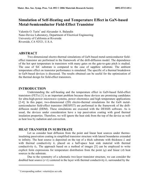
0892-FF13-05.3Figure 2. <strong>GaN</strong> MESFET current-voltage (a) <strong>and</strong> maximum temperature-voltage (b) characteristics obta<strong>in</strong>ed byelectro-thermal simulations for transistor with substrate lengths 50 µm, 100µm, 200 µm <strong>and</strong> 3 mm for theisothermal boundary condition <strong>of</strong> 300 K on the substrate bottom. Dash curve on (a) is for the case <strong>of</strong> theisothermal simulation. For all curves the source - gate bias is zero. Arrow shows the <strong>in</strong>crease <strong>of</strong> substrate length.On <strong>in</strong>set to figure (a) you can see schematic cross-section <strong>of</strong> the considered <strong>GaN</strong> MESFET. Inset to figure (b)shows the elementary cell <strong>of</strong> transistor with many gate f<strong>in</strong>gers with marked simulation doma<strong>in</strong>.The dimension <strong>of</strong> the heat spread<strong>in</strong>g <strong>in</strong> a substrate <strong>in</strong>creases rapidly as the thermalconductivity <strong>of</strong> the heat s<strong>in</strong>k becomes equal or less than the thermal conductivity <strong>of</strong> thesubstrate. In the characteristic case <strong>of</strong> K = 1 (k 1 = k 2 ) calculations for the case <strong>of</strong> a po<strong>in</strong>t heatsource gives the diameter <strong>of</strong> the 0.9 WHF through the substrate bottom equal to 19.9L. For thel<strong>in</strong>ear heat source, we have a size <strong>of</strong> 0.9 WHF through the substrate bottom equal to 12.6L.Hence, for the case <strong>of</strong> the same thermal conductivities <strong>of</strong> two layers, the dimension <strong>of</strong> the heatspread<strong>in</strong>g at substrate bottom is about 10 to 20 times larger than the substrate thickness.A typical field effect transistor have a f<strong>in</strong>ite width <strong>of</strong> the active channel, so thedistribution <strong>of</strong> the temperature <strong>and</strong> the heat flow <strong>in</strong> the real devices would be someth<strong>in</strong>gbetween two considered cases <strong>of</strong> po<strong>in</strong>t <strong>and</strong> l<strong>in</strong>ear heat sources. Hence, we can conclude thatfor simulations without significant distortion <strong>of</strong> a heat flow <strong>in</strong> the transistor substrate with aperfect heat s<strong>in</strong>k from the substrate bottom surface (isothermal boundary condition), we need asimulation doma<strong>in</strong> with a substrate length more than substrate thickness.SIMULATION DETAILSAll simulations are performed for the follow<strong>in</strong>g parameters <strong>of</strong> the device <strong>based</strong> on theactual <strong>GaN</strong> MESFET described <strong>in</strong> [6]. The dop<strong>in</strong>g concentration <strong>in</strong> the active layer is 3⋅10 17cm -3 ; the thickness <strong>of</strong> the active layer is 200 nm; the source - dra<strong>in</strong> separation 5 µm; <strong>and</strong> thegate length 1.5 µm. The n-type <strong>GaN</strong> active layer is deposited on the top <strong>of</strong> a 3 µm thick semi<strong>in</strong>sulat<strong>in</strong>g(SI) <strong>GaN</strong> buffer (a schematic picture <strong>of</strong> simulated <strong>GaN</strong>-<strong>based</strong> MESFET is shown on<strong>in</strong>set to Fig. 2(a)). Although the transistor described <strong>in</strong> [6] has a sapphire substrate, <strong>in</strong> thiswork, we consider the case <strong>of</strong> a 300 µm thick SiC substrate. SiC has a high thermalconductivity coefficient at room temperature k SiC = 3.3 Wcm -1 K -1 , hence it is a promis<strong>in</strong>gmaterial for <strong>GaN</strong> transistors substrates. We take k <strong>GaN</strong> =1.6 Wcm -1 K -1 <strong>and</strong> k sapph =0.35 Wcm -1 K -1 .The T -0.5 temperature dependence for thermal conductivity <strong>of</strong> <strong>GaN</strong> <strong>and</strong> T -1 for SiC <strong>and</strong>sapphire has been taken <strong>in</strong>to account <strong>in</strong> the presented simulations. Boundary conditions on
0892-FF13-05.4Figure 3. Dependence <strong>of</strong> the maximumtemperature on the substrate length for thecase <strong>of</strong> isothermal (R th = 0.0 K cm 2 /W) <strong>and</strong>convective (R th = 0.1 K cm 2 /W) boundaryconditions on the substrate bottom. Ambienttemperature is 300 K. The source-dra<strong>in</strong> biasis 50 V <strong>and</strong> the source-gate bias is zero.Figure 4. Electro-thermal simulations <strong>of</strong> theambient temperature effect on outputcharacteristics for <strong>GaN</strong> MESFET on SiCsubstrate with 3 mm length. Thermalresistance <strong>of</strong> 0.1 Kcm 2 /W lumped to substratebottom. Set <strong>of</strong> different substrate bottomtemperatures is from 0 o C to 500 o C with100 o C step. Dot curves correspond to thecase <strong>of</strong> 300 K. Source-gate bias is zero.Figure 5. Upper curve, marked AB, is forisothermal simulation (T = 300 K) for <strong>GaN</strong>MESFET with beg<strong>in</strong>n<strong>in</strong>g <strong>of</strong> avalanchebreakdown at dra<strong>in</strong>. Lower curve, markedTB, is for electro-thermal simulation withthermal resistance <strong>of</strong> 0.1 K cm 2 /W lumped tosubstrate bottom <strong>and</strong> for 1 mm SiC substratelength. Source-gate bias is zero for bothcases. Dot curve shows respective maximumtemperature-voltage characteristic for electrothermalsimulation.boundaries without contacts (particularly lateral boundaries) are <strong>of</strong> reflective type that givesthe zero normal components <strong>of</strong> electric field, electrons <strong>and</strong> holes current, <strong>and</strong> heat flow. That iswhy we can consider simulated one-gate doma<strong>in</strong> as half <strong>of</strong> elementary cell <strong>of</strong> transistor withmany gate f<strong>in</strong>gers (see <strong>in</strong>set to Fig. 2b). Other details about used boundary conditions aredescribed elsewhere (see TCAD DESSIS manual <strong>and</strong> [7]). We assume the Schottky barrierpotential height to be 1 eV. For the low-field mobility dependence on temperature <strong>and</strong> dop<strong>in</strong>gconcentration, a model [8] specific for <strong>GaN</strong> has been used. The new modified transferred-
0892-FF13-05.5electron (MTE) model that is able to replicate the specific electric field dependence <strong>of</strong> the driftvelocity <strong>of</strong> electrons <strong>in</strong> <strong>GaN</strong> has been used [9]. Saturation velocity 1.91 x 10 7 cm/s for 300 Ktemperature was extracted from the Monte-Carlo simulation results [10]. The l<strong>in</strong>eardependence <strong>of</strong> saturation velocity on temperature was considered with negative temperaturecoefficient -6.33 x 10 3 cm s -1 K -1 , that was obta<strong>in</strong>ed by fitt<strong>in</strong>g the data from the Monte Carlosimulations [11].DISCUSSION<strong>Simulation</strong>s for different substrate lengths <strong>in</strong> the case <strong>of</strong> an isothermal boundarycondition on substrate bottom surface are shown on Fig. 2. For the case <strong>of</strong> electro-thermalsimulations <strong>of</strong> transistor on SiC substrate with 50 µm substrate length, we can see significantdegradation <strong>of</strong> output characteristics with pronounced NDC region <strong>and</strong> with relatively hightemperature <strong>of</strong> the hot spot. Degradation <strong>of</strong> output characteristics <strong>in</strong> the case <strong>of</strong> 3 mm substratelength is less pronounced. Obta<strong>in</strong>ed results are <strong>in</strong> qualitative agreement with results published<strong>in</strong> Ref. [12,13]. Dash curve on Fig. 2a presents isothermal simulations without NDC.The top curve on Fig. 3 expla<strong>in</strong>s how a non-ideal heat s<strong>in</strong>k <strong>in</strong>fluences hot spottemperature. In the case <strong>of</strong> a convective boundary condition on substrate bottom, with typicalvalue <strong>of</strong> package thermal resistance R th = 0.1 Kcm 2 /W the saturation value <strong>of</strong> a maximumtemperature <strong>of</strong> hot spot for zero source-gate bias <strong>and</strong> 50 volts source-dra<strong>in</strong> bias is 190 o C,which is only 40 o C higher than one for the case <strong>of</strong> an ideal heat s<strong>in</strong>k. Note that temperaturesaturation occurs at 3 mm substrate length that is order <strong>of</strong> magnitude larger than for the case <strong>of</strong>an isothermal boundary condition.<strong>Simulation</strong>s for the case <strong>of</strong> sapphire substrate show that the degradation <strong>of</strong> outputcharacteristics <strong>and</strong> temperature <strong>of</strong> the hot spot is significantly larger than for the case <strong>of</strong> SiCsubstrate. For example, for the case <strong>of</strong> zero source-gate bias <strong>and</strong> for 50 volts source-dra<strong>in</strong> bias,the temperature <strong>of</strong> the hot spot <strong>in</strong> the case <strong>of</strong> sapphire substrate is 250 o C, which is 100 o C largerthan <strong>in</strong> the case <strong>of</strong> SiC substrate.On Fig. 4 simulation <strong>of</strong> temperature effect is presented. <strong>Simulation</strong>s <strong>in</strong>dicates ~ 40%degradation <strong>in</strong> the saturation current with temperature <strong>in</strong>crease from room temperature to250 o C that is <strong>in</strong> good agreement with experimental data [7].In addition, we have studied breakdown <strong>in</strong> <strong>GaN</strong>-<strong>based</strong> field-effect transistors. In FETs,the most common type <strong>of</strong> breakdown is avalanche breakdown under the dra<strong>in</strong>-side edge <strong>of</strong> thegate. However, <strong>in</strong> modern devices an advanced gate-design solutions, such as a recessed gate,passivation, <strong>and</strong> a gate with a field plate, are used to <strong>in</strong>crease gate breakdown voltage. Inaddition, <strong>GaN</strong>-<strong>based</strong> metal-<strong>in</strong>sulator-semiconductor field-effect transistor (MISFET) ispromis<strong>in</strong>g devices with significantly decreased gate leakage current. Hence, anybody cansuggest that the fundamental limit on field-effect transistor performance is the avalanchebreakdown at dra<strong>in</strong>. Moreover, our simulations show that, this take place for Si <strong>and</strong> GaAs<strong>based</strong>FETs. However, <strong>in</strong> <strong>GaN</strong>, that is wide b<strong>and</strong> gap semiconductor, breakdown electric fieldorder <strong>of</strong> magnitude higher than <strong>in</strong> Si <strong>and</strong> GaAs. Hence, avalanche dra<strong>in</strong> breakdown <strong>in</strong> <strong>GaN</strong>FETs should occur at much more higher voltages <strong>in</strong> comparison with Si <strong>and</strong> GaAscounterparts. Here question arises: can thermal breakdown <strong>in</strong> <strong>GaN</strong>-<strong>based</strong> FETs occur beforedevelopment <strong>of</strong> avalanche at dra<strong>in</strong>?Upper curve on Fig. 5 shows isothermal simulations with beg<strong>in</strong>n<strong>in</strong>g <strong>of</strong> avalanchebreakdown (AB) at dra<strong>in</strong> about 400 V source-dra<strong>in</strong> bias. Lower curve shows electro-thermal
0892-FF13-05.6simulation with beg<strong>in</strong>n<strong>in</strong>g <strong>of</strong> thermal breakdown (TB) at about 200 V source-dra<strong>in</strong> bias. Inmore harsh thermal conditions, thermal breakdown voltage can be even less [14]. Hence, wecan conclude that the temperature <strong>of</strong> hot spot <strong>in</strong> active channel <strong>of</strong> <strong>GaN</strong> FETs can rise up to<strong>in</strong>tr<strong>in</strong>sic <strong>GaN</strong> temperature estimated by Neudeck et al. [15]. At the same time, due to the highvalue <strong>of</strong> <strong>GaN</strong> breakdown field, the device can be far from the beg<strong>in</strong>n<strong>in</strong>g <strong>of</strong> avalanche or Zenerbreakdown. We can suppose that <strong>in</strong> such conditions, thermal generation <strong>of</strong> carriers can lead tothermal <strong>in</strong>stabilities or even to development <strong>of</strong> irreversible thermal breakdown. Note that one<strong>of</strong> the most promis<strong>in</strong>g applications <strong>of</strong> <strong>GaN</strong>-<strong>based</strong> devices is high temperature electronics forambient temperatures beyond 300 o C [15]. In such harsh conditions <strong>of</strong> operation, thermalbreakdown can be the dom<strong>in</strong>ant fault mechanism for <strong>GaN</strong>-<strong>based</strong> FETs.CONCLUSIONSThe electro-thermal simulations performed for the <strong>GaN</strong> MESFET with many gates <strong>and</strong>with thermo-<strong>in</strong>sulat<strong>in</strong>g passivation show that the gate-to-gate pitch should be larger than thesubstrate thickness to obta<strong>in</strong> a m<strong>in</strong>imum hot spot temperature. We conclude that the negativedifferential conductivity on output characteristics resulted from a degradation <strong>of</strong> electronmobility associated with an <strong>in</strong>crease <strong>of</strong> the hot spot temperature <strong>in</strong> the transistor channel.<strong>Simulation</strong> <strong>of</strong> the ambient temperature effect <strong>in</strong>dicates significant degradation <strong>in</strong> the saturationcurrent with temperature <strong>in</strong>crease. We suppose that <strong>in</strong> <strong>GaN</strong>-<strong>based</strong> FETs thermal breakdowncan be dom<strong>in</strong>ant fault mechanism.ACKNOWLEDGMENTSThe work at UCR has been supported <strong>in</strong> part by the grants to AAB from the Office <strong>of</strong>Naval Research (ONR), National Science Foundation (NSF) <strong>and</strong> US CRDF. The authorsacknowledge SYNOPSYS Company for donat<strong>in</strong>g a new release <strong>of</strong> DESSIS s<strong>of</strong>tware (formerISE TCAD) to carry out the simulations described <strong>in</strong> this work.REFERENCES1. M.A. Khan et al., Appl. Phys. Lett. 62, 1786 (1993); 63, 1214 (1993).2. Y.-F. Wu, IEEE Electron Device Lett. 25, 117 (2004).3. A.A. Bal<strong>and</strong><strong>in</strong> et al., IEEE Electron Device Lett. 19, 475 (1998).4. S. Yoshida et al., Solid-State Electron 47, 589 (2003).5. N. R<strong>in</strong>aldi, IEEE Trans. Electron Device 49, 679 (2002).6. S.C. B<strong>in</strong>ari et al., Solid-State Electron 41, 1549 (1997).7. W.L. Liu et al., MRS Internet J. Nitride Semicond. Res. 9, 7 (2004).8. T.T. Mnatsakanov et al., Solid-State Electron. 47, 111 (2003).9. V.O. Tur<strong>in</strong>, Solid-State Electron. 49, 1678 (2005).10. M. Farahm<strong>and</strong> et al., IEEE Trans. Electron Devices, 48, 535 (2001).11. U.V. Bhapkar <strong>and</strong> M.S. Shur, J. Appl. Phys. 82, 1649 (1997).12. M. Kuball et al., phys. stat. sol. (a) 202, 824 (2005).13. S. Nutt<strong>in</strong>ck et al., IEEE Trans. Microwave Theory Tech. 51, 2445 (2003).14. V.O. Tur<strong>in</strong> <strong>and</strong> A.A. Bal<strong>and</strong><strong>in</strong>, Electron. Lett. 40, 81 (2004).15. P.G. Neudeck, R.S. Okojie, <strong>and</strong> L.-Y. Chen, Proc. IEEE, 90, 1065 (2002).