Design of a Low-Power High-Speed T-Flip- Flop Using ... - Telfor 2009
Design of a Low-Power High-Speed T-Flip- Flop Using ... - Telfor 2009
Design of a Low-Power High-Speed T-Flip- Flop Using ... - Telfor 2009
- No tags were found...

You also want an ePaper? Increase the reach of your titles
YUMPU automatically turns print PDFs into web optimized ePapers that Google loves.
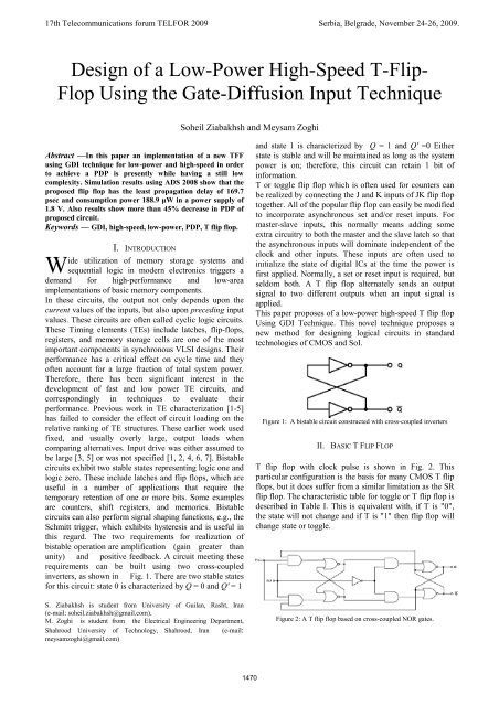
TABLE I: THE CHARACTERISTIC TABLE FOR A TOGGLE ORT FLIP FLOP.T Q(t+1)No Change 0 Q(t)Toggle 1 Q'(t)III. BASIC GDI FUNCTIONThe GDI method is based on the simple cell shown inFig. 3. A basic GDI cell contains four terminals - G (thecommon gate input <strong>of</strong> the nMOS and pMOS transistors), P(the outer diffusion node <strong>of</strong> the pMOS transistor), N (theouter diffusion node <strong>of</strong> the nMOS transistor) and the Dnode (the common diffusion <strong>of</strong> both transistors). P, N andD may be used as either input or output ports, dependingon the circuit structure. Table II shows how variousconfiguration changes <strong>of</strong> the inputs P, N and G in the basicGDI cell correspond to different Boolean functions at theoutput D. GDI enables simpler gates, lower transistorcount, and lower power dissipation in manyimplementations, as compared with standard CMOS andPass-transistor Logic (PTL) design techniques [8].latch. The components <strong>of</strong> the latch circuit can be dividedinto two main categories; GDI gate and inverter. GDI gateuses two transistors and controlled by the Clk signal. Clksignals fed to the gate <strong>of</strong> transistors and create twoalternative states: one state is when the Clk is low and thesignals are propagating through PMOS transistors andcreate transient state and other one is when the Clk is highand the prior values are maintained due to conduction <strong>of</strong>the outputs. In this state, GDI gates holding state <strong>of</strong> thelatch.Other gates for main T flip flop are inverter gates. Theyare responsible for maintaining the complementary values<strong>of</strong> the internal signals and the circuit outputs. Note that thesize <strong>of</strong> the p-channel transistor is wider than that <strong>of</strong> the n-channel transistor. This width difference is not needed forfunctionally correct operation. Rather, it somewhatcompensates for the difference in the motilities <strong>of</strong> n-channel and p-channel transistors. The effective mobility<strong>of</strong> n-channel transistors is between two and four times that<strong>of</strong> p-channel transistors. These inverters has important rolefor swing restoration and improved driving abilities <strong>of</strong> theoutputs, it's buffering <strong>of</strong> the internal signals and createsuitable output current for driving <strong>of</strong> load.Figure 3: GDI basic cellTABLE II: SOME LOGIC FUNCTIONS THAT CAN BEIMPLENTED WITH A SINGLE GDI CELL.N P G D Function'0' B A HB F1B '1' A H + B F2'1' B A A + B ORB '0' A AB ANDC B A HB+AC MUX'0' '1' A H NOTThis paper presents a new implementation <strong>of</strong> low-power,high-speed TFF using GDI technique. This new designachieves lower PDP in compared with previous works. Thecircuits have been implemented in 0.18 Km TSMC CMOStechnology and simulated to the proposed GDI structurewith existing alternatives.Figure 4: GDI T flip flop implementation.V. SIMULATION RESULTSA T flip flop designed in GDI and two kinds <strong>of</strong> CMOS wassimulated in 0.18Km TSMC CMOS [9] technology.Simulation results shows compare the GDI design with aset <strong>of</strong> representative flip flops, commonly used for highperformance design. The circuits were simulated usingADS 2008 at 1.8V, 500 MHz and 27 0 c, with loadcapacitance <strong>of</strong> 100fF. The simulation setup is shown inFig. 5. The device under test was placed between inputbuffers to account for the current consumption from theprevious stage, and output buffers to emulate realenvironmental conditions.IV. DESIGN OF LOW-POWER, HIGH-SPEED GDIT FLIP FLOPA novel implementation <strong>of</strong> a GDI TFF is shown in Fig. 4.It is based on the Master-Slave connection <strong>of</strong> two GDILatches and some gates. Each latch consists <strong>of</strong> four basicGDI cells, resulting in a simple eight-transistor structureand gates consists six transistors in order that related with1471
Figure 5: Simulation setup.The reference circuits are presented in Fig. 6. The setincludes (a) modified CMOS after and (b) TGB after [10].These circuits have been sized according to optimizationprocedure, as presented in [10].Fig. 8 shows timing diagram <strong>of</strong> input clock, square inputwave, output <strong>of</strong> T flip flop (Q) and its differential output(Q') for proposed T flip flop. The comparative results arepresented in Table III. The best results in each comparedcategory are emphasized. It can be seen, that GDI TFFoutperforms the other circuits in terms <strong>of</strong> power-delayproduct and total gates area in both technologies (includingthe inverted inputs).1) Average <strong>Power</strong>: Best results <strong>of</strong> average power areobserved for the dynamic GDI ~ 77 % (approximately)less than the modified CMOS implementation and 84%less than the TGB circuit (which is the best CMOSimplementation in terms <strong>of</strong> power). GDI T flip flop showresults close to the CMOS circuit, and better than anystatic CMOS implementation.2) Maximal Delay: The Dynamic GDI is the fastest circuit,showing up to 44% decrease compared to modified CMOStechniques, and a 76% improvement compared to theTGB, which is the fastest technique among CMOS circuits.3) <strong>Power</strong> delay product: GDI T flip flop circuit has 87%decrease PDP compared to modified CMOS technique and96% less than TGB circuit.It should be noted that the optimization in all comparedcircuits is performance-driven (minimal power-delayproduct is obtained by sizing), while separate parameters,like average power and maximal delay are secondary. TheSimulation results diagram obtained through can be seen inFig. 8 for Average power and PDP used.The layout <strong>of</strong> the proposed low-power, high-speed TFF ispresented in Fig. 9.(b)Figure 6: Set <strong>of</strong> representative flip-flops for comparison: (a) modifiedCMOS, (b) TGB(a)(b)(c)(d)Figure 7: timing diagram <strong>of</strong> a) input clock, b) square input wave, c)output <strong>of</strong> T flip flop (Q) and d) differential output (Q')(a)(a)1472
on iterative transistor sizing, while targeting a minimalpower-delay product. Performance comparison with otherTFF design techniques was shown, with respect to gatearea, delay and power dissipation.Simulation results in 0.18 µm CMOS process show that theproposed T flip flop has the least propagation delay <strong>of</strong>169.7 psec, consumption power 188.9 µW and powerdelay product 32.05fJ in a power supply <strong>of</strong> 1.8 V.(b)Figure 8: Simulation results diagram and comparison <strong>of</strong> modifiedCMOS, TGB and GDI for a)Average power and b) PDP used.Figure 9: Proposed CMOS T flip flop layout.VI. CONCLUSIONA novel methodology for asynchronous circuits, based ontwo-transistor GDI cells, was presented. In this paper weproposed a GDI T flip flop for low-power design waspresented. The proposed circuit has a simple structure,based on two Master-Slave principles, and some gates todescribe T flip flop. It contains 24 transistors. Anoptimization procedure was developed for GDI TFF, basedREFERENCES[1] H. Kawaguchi and T. Sakurai. A reduced clock-swing flipflop(RCSFF) for 63%power reduction. IEEE Journal Solid-StateCircuits, 33(5):807–811, May 1998.[2] U. Ko and P. Balsara. <strong>High</strong> performance, energy-efficient D flipflopcircuits. IEEE Trans. VLSI Systems, 8(1):94–98, February2000.[3] B. Nikoli´c, V. OklobdSzija, V. Stojanovi´c,W. Jia, J. Chiu, and M.Leung. Improved sense-amplifier-based flip-flop: <strong>Design</strong> andmeasurements. IEEE Journal <strong>of</strong> Solid-State Circuits, 35(6):876–884, June 2000.[4] M. Nogawa and Y. Ohtomo. A data-transition look-ahead DFFcircuit for statistical reduction in power consumption. IEEEJournal Solid-State Circuits, 33(5):702–706, May 1998.[5] V. Stojanovi´c and V. OklobdSzija. Comparative analysis <strong>of</strong>master-slave latches and flip-flops for high-performance and lowpowersystems. IEEE Journal Solid-State Circuits, 34(4):536–548,April 1999.[6] T. Lang, E. Musoli, and J. Cortadella. Individual flip-flops withgated clocks for low power datapaths. IEEE Trans. Circuits andSystems-II: Analog and Digital Signal Processing, 44(6):507–516,June 1997.[7] V. Zyuban and P. Kogge. Application <strong>of</strong> STD to latchpowerestimation. IEEE Trans. VLSI Systems, 7(1):111–115, March 1999.[8] A. Morgenshtein, A. Fish, I.A. Wagner, “Gate-Diffusion Input(GDI) – A <strong>Power</strong> Efficient Method for Digital CombinatorialCircuits,” IEEE Trans. VLSI, vol. 10, no. 5, pp. 566-581, October2002.[9] MOSIS, http://www.mosis.org.[10] Ken Martin, "Digital Integrated Circuit <strong>Design</strong>", Oxford universitypress, 2000.CircuitNumber <strong>of</strong>TransistorsTABLE III: SIMULATION RESULTS FOR 0.18µm TSMC CMOS TECHNOLOGY.TotalWidth[=m]CLK- Q(LH)[ps]CLK- Q'(HL)[ps]CLK- Q(HL)[ps]CLK- Q'(LH)[ps]<strong>Power</strong>[=m]MaxDelay[ps]ModifiedCMOS24 36.9 301.2 134 122.9 145.4 827.48 301.2 249.23TGB 26 41.76 715 126.5 124.1 132.8 1189.15 715 850.24GDI 24 6.82 131.6 167.5 169.7 168.5 188.88 169.7 32.05TotalPDP[fJ]1473