Ecv doping profile measurements of aluminium
Ecv doping profile measurements of aluminium
Ecv doping profile measurements of aluminium

Create successful ePaper yourself
Turn your PDF publications into a flip-book with our unique Google optimized e-Paper software.
20 th European Photovoltaic Solar Energy Conference and Exhibition, Barcelona, 6-10 June 2005<br />
Pre-Print, 2DV2.48<br />
ECV DOPING PROFILE MEASUREMENTS OF ALUMINIUM ALLOYED BACK SURFACE FIELDS<br />
F. Huster and G. Schubert<br />
University <strong>of</strong> Konstanz, Department <strong>of</strong> Physics, 78457 Konstanz, Germany<br />
email: frank.huster@uni-konstanz.de<br />
ABSTRACT: A comprehensive study <strong>of</strong> the <strong>doping</strong> <strong>pr<strong>of</strong>ile</strong>s <strong>of</strong> <strong>aluminium</strong> alloyed (screen printed and RTP fired)<br />
back surface field (BSF) layers in crystalline silicon is presented, based on the electrochemical capacitance-voltage<br />
(ECV) <strong>pr<strong>of</strong>ile</strong> measuring technique combined with an advanced evaluation. Precise <strong>measurements</strong> <strong>of</strong> pure Al <strong>pr<strong>of</strong>ile</strong>s<br />
are compared with simulations made using the Al-Si phase diagram. The contribution <strong>of</strong> boron <strong>doping</strong> from the glass<br />
frit and the dependence <strong>of</strong> BSF formation on crystal orientation investigated. The importance <strong>of</strong> incomplete<br />
ionization <strong>of</strong> Al atoms at room temperature is introduced.<br />
Keywords: Aluminium, Back Surface Field, Doping Pr<strong>of</strong>ile<br />
1 INTRODUCTION<br />
“Carrier <strong>pr<strong>of</strong>ile</strong> engineering” is needed to further<br />
optimize the properties <strong>of</strong> the <strong>aluminium</strong> alloyed back<br />
surface field beyond the usual empirical approach. The<br />
electrical properties <strong>of</strong> the BSF are determined by the<br />
<strong>doping</strong> level, the <strong>doping</strong> <strong>pr<strong>of</strong>ile</strong>, lateral inhomogeneities<br />
and defects. The first three issues are addressed in this<br />
work. The results are intended to provide new knowledge<br />
and tools for <strong>pr<strong>of</strong>ile</strong> engineering and thereby help to<br />
close the gap between actual and theoretical best BSF<br />
performance.<br />
The ECV (electrochemical capacitance voltage)<br />
technique is well suited for carrier <strong>pr<strong>of</strong>ile</strong> <strong>measurements</strong>.<br />
When applied with care and advanced evaluation<br />
procedures as described in sections 3 to 5, <strong>pr<strong>of</strong>ile</strong><br />
<strong>measurements</strong> with a high absolute accuracy can be<br />
obtained.<br />
2 EXPERIMENTAL<br />
The four screen printable Al pastes listed in Table I<br />
were used. They were printed onto polished FZ silicon<br />
and fired in an RTP furnace for BSF formation. The<br />
exact paste compositions are not disclosed by the paste<br />
manufacturers. The frit contents are estimated from<br />
safety data sheets and the results found in this work.<br />
Pastes A and D are not commercially available.<br />
Paste Assumed glass<br />
frit content<br />
Boron?<br />
A “pure” Al Very low Very low<br />
B Ferro Medium In glass<br />
53-038<br />
frit<br />
C DuPont High In glass<br />
PV331<br />
frit<br />
D Al +3% B Medium 3% added<br />
Table I: Al pastes used in this work. The content <strong>of</strong> lead<br />
borosilicate glass is in the range <strong>of</strong> a few wt-%.<br />
The ECV <strong>measurements</strong> were performed using an<br />
Accent PN4300PC <strong>pr<strong>of</strong>ile</strong>r. The measurement spot was<br />
defined by a sealing ring <strong>of</strong> 3.5 mm in diameter. The<br />
electrolyte used was 0.1 M NaH 5F 2 solution and an<br />
effective dissolution valence <strong>of</strong> z = 3.7 was assumed. For<br />
details on the measurement technique see [1] and<br />
references therein.<br />
Page 1<br />
3 EVALUATION OF ECV MEASUREMENTS<br />
To obtain a “real” concentration <strong>pr<strong>of</strong>ile</strong> from an ECV<br />
measurement, corrections for several effects have to be<br />
made. A program was therefore developed by which<br />
ECV <strong>measurements</strong> <strong>of</strong> BSF <strong>pr<strong>of</strong>ile</strong>s can be simulated on<br />
the basis <strong>of</strong> a tentative real <strong>pr<strong>of</strong>ile</strong> (or a lateral <strong>pr<strong>of</strong>ile</strong><br />
distribution, see section 4). By fitting this simulation to<br />
the measurement, the real <strong>pr<strong>of</strong>ile</strong> can be obtained. The<br />
following effects are taken into account:<br />
• Surface roughness: The wavy surface <strong>of</strong> an alloyed<br />
BSF has an area larger than a planar surface by a<br />
factor <strong>of</strong> 1.01 to 1.1. The measured concentration is<br />
proportional to the square <strong>of</strong> this enlargement factor.<br />
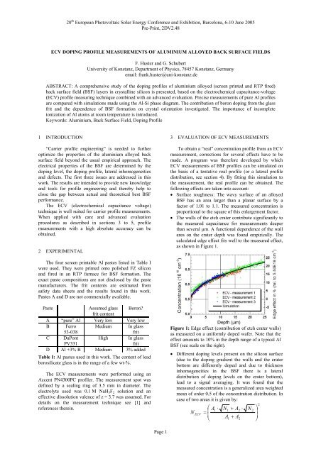
• The walls <strong>of</strong> the etch crater contribute significantly to<br />
the measured capacitance for <strong>measurements</strong> deeper<br />
than several µm. A functional dependence <strong>of</strong> the wall<br />
area on the crater depth was found empirically. The<br />
calculated edge effect fits well to the measured effect,<br />
as shown in Figure 1.<br />
Figure 1: Edge effect (contribution <strong>of</strong> etch crater walls)<br />
as measured on a uniformly doped wafer. Note that the<br />
effect amounts to 10% in the depth range <strong>of</strong> a typical Al<br />
BSF (see scale on the right).<br />
• Different <strong>doping</strong> levels present on the silicon surface<br />
(due to the <strong>doping</strong> gradient the walls and the crater<br />
bottom are differently doped and due to thickness<br />
inhomogeneities in the BSF there is a lateral<br />
distribution <strong>of</strong> <strong>doping</strong> levels on the crater bottom),<br />
lead to a signal averaging. It was found that the<br />
measured concentration is a generalized area weighted<br />
mean <strong>of</strong> order 0.5 <strong>of</strong> the concentration distribution. In<br />
case <strong>of</strong> two areas it is given by:<br />
2<br />
⎛ A1<br />
⋅ N1<br />
+ A ⎞<br />
2 ⋅ N<br />
⎜<br />
2<br />
N ⎟<br />
ECV<br />
=<br />
⎜<br />
⎟<br />
⎝<br />
A1<br />
+ A2<br />
⎠
20 th European Photovoltaic Solar Energy Conference and Exhibition, Barcelona, 6-10 June 2005<br />
Pre-Print, 2DV2.48<br />
BSF THICKNESS INHOMOGENEITY<br />
Figure 2 shows a BSF <strong>pr<strong>of</strong>ile</strong> measured using ECV,<br />
the simulated <strong>pr<strong>of</strong>ile</strong> fitted to this result and the<br />
underlying real <strong>pr<strong>of</strong>ile</strong> determined from the simulation.<br />
The rounded inner edge <strong>of</strong> the measured ECV <strong>pr<strong>of</strong>ile</strong> can<br />
be modelled by assuming a Gaussian BSF thickness<br />
distribution and applying the mathematical procedures<br />
discussed in section 3.<br />
Figure 2: ECV measurement and <strong>pr<strong>of</strong>ile</strong> simulation for<br />
the same sample as shown in Figure 3.<br />
To verify this model, the thickness distribution <strong>of</strong> a<br />
BSF cross-section was measured by cleaving and staining<br />
in 1:3:6 (HF:HNO3:CH3COOH) etch. In Figure 3, this<br />
distribution and a Gaussian fit for a sample fired at<br />
825°C for 1 s (13.4 mg/cm 2 Al, paste B) is shown. This is<br />
the same sample for which the ECV measurement is<br />
shown in Figure 2.<br />
Figure 3a,3b: Direct<br />
measurement <strong>of</strong> the BSF<br />
thickness distribution<br />
using optical microscope<br />
pictures <strong>of</strong> BSF crosssections.<br />
A Gaussian<br />
distribution is fitted to the<br />
<strong>measurements</strong>.<br />
Because the thickness inhomogeneities on a lateral<br />
scale are much smaller than the size <strong>of</strong> the measurement<br />
spot, an effective averaging is included in the ECV<br />
<strong>measurements</strong>. Taking into account the corrections listed<br />
in section 3, an ECV <strong>pr<strong>of</strong>ile</strong> can be calculated and fitted<br />
to the measurement, here with the BSF thickness and<br />
standard deviation as fitting parameters. There are two<br />
significant results: Firstly, the calculated curve fits well<br />
to the measurement, yielding a Gaussian distribution in<br />
good agreement with that obtained from a direct<br />
thickness measurement (Figure 3). Secondly, a real<br />
concentration <strong>pr<strong>of</strong>ile</strong> is obtained, representing that which<br />
would have been measured without thickness<br />
inhomogeneities and without measurement technique<br />
related effects. The local BSF <strong>pr<strong>of</strong>ile</strong>s are assumed to<br />
have the shape <strong>of</strong> this real <strong>pr<strong>of</strong>ile</strong>, only differing in depth<br />
according to the Gaussian distribution.<br />
The ECV measurement technique combined with this<br />
evaluation procedure is therefore able to quantify the<br />
thickness inhomogeneities <strong>of</strong> an alloyed BSF. In Table II<br />
optical microscope pictures <strong>of</strong> three BSF <strong>pr<strong>of</strong>ile</strong>s are<br />
shown. The thickness inhomogeneity and the surface<br />
Page 2<br />
roughness are considerably reduced by using a larger<br />
amount <strong>of</strong> deposited <strong>aluminium</strong>. Interestingly the BSF<br />
thickness seems to saturate at about 10 µm on (100)<br />
oriented silicon using standard firing parameters.<br />
BSF thickness (from ECV)<br />
Al (mg/cm 2 )<br />
Average (µm) Gauss.stand.dev. %<br />
5.9 6.3 20.0<br />
13.4 9.9 9.4<br />
28.1 9.5 5.0<br />
Table II: Optical microscope pictures <strong>of</strong> Al-BSF crosssections.<br />
Paste B, fired at 825°C for 1 s, ramp up and<br />
down by 20 K/s. Substrate: polished (100) FZ silicon.<br />
4 WHAT IS ACTUALLY MEASURED BY ECV?<br />
In the <strong>doping</strong> range <strong>of</strong> 10 17 to 10 19 cm -3 , incomplete<br />
ionization <strong>of</strong> dopant atoms is present even at room<br />
temperature. This interesting, yet <strong>of</strong>ten neglected effect<br />
[2, 3], is especially important for investigations <strong>of</strong> Al<br />
BSFs since the Al <strong>doping</strong> concentration lies in the<br />
relevant range and the higher ionization energy <strong>of</strong> Al<br />
compared to shallow dopants like B (69 meV to 44 meV)<br />
causes a large effect. As neither experimental<br />
investigations nor calculations <strong>of</strong> incomplete ionization<br />
in Al doped silicon were found in the literature,<br />
calculations were done to estimate the relevance <strong>of</strong> this<br />
effect for the Al BSF. The results are shown in Figure 4<br />
and should be read as qualitative as the physics <strong>of</strong> highly<br />
doped silicon is involved and still a topic <strong>of</strong> fundamental<br />
solid state research. It is expected from this calculation<br />
that 20 to 50% <strong>of</strong> the substitutional Al atoms do not<br />
contribute to the hole concentration.<br />
Figure 4: Calculated fraction <strong>of</strong> ionized substitutional<br />
dopant atoms at 300 K. At low concentrations and also at<br />
high concentrations above the metal-insulator(MI)transition<br />
the atoms are fully ionized. The <strong>doping</strong> range<br />
<strong>of</strong> the MI-transition for Al and In is not well known.<br />
In view <strong>of</strong> the incomplete ionization, it is important<br />
to clarify what concentration is measured by capacitancevoltage<br />
techniques. The concentration is determined by<br />
measuring the differential capacity on varying the reverse<br />
biased voltage across a rectifying junction. The band<br />
bending (or equivalently the high electric field) in the<br />
depletion region leads to a complete ionization <strong>of</strong> the<br />
dopant atoms [4]. Therefore by the ECV technique the
20 th European Photovoltaic Solar Energy Conference and Exhibition, Barcelona, 6-10 June 2005<br />
Pre-Print, 2DV2.48<br />
concentration <strong>of</strong> all substitutional Al atoms is measured.<br />
For the solar cell operation the carrier <strong>pr<strong>of</strong>ile</strong> is<br />
important, which is lower according to the degree <strong>of</strong><br />
incomplete ionization.<br />
The effect <strong>of</strong> incomplete ionization should appear as<br />
a difference in the measured BSF sheet resistance and<br />
that calculated from an ECV <strong>pr<strong>of</strong>ile</strong>. Results for the 4<br />
pastes investigated in this work are shown in Table III.<br />
Sheet resistance (Ohm/sq)<br />
BSF made from<br />
Measured Calculated from<br />
paste …<br />
(4 PP) ECV <strong>pr<strong>of</strong>ile</strong><br />
A (“pure” Al) 25.3 15.0<br />
B (B in glass frit) 11.0 8.7<br />
C (B in glass frit) 3.0 2.7<br />
D (B added) 2.7 2.7<br />
Table III: Comparison <strong>of</strong> BSF sheet resistances<br />
obtained directly and from ECV <strong>pr<strong>of</strong>ile</strong>s. As expected,<br />
with a pure Al paste, the effect <strong>of</strong> incomplete ionization<br />
appears to be significant.<br />
While for the <strong>pr<strong>of</strong>ile</strong>s that are dominated by boron<br />
<strong>doping</strong> (pastes B, C, and D) a good agreement is found<br />
(i.e., the concentration <strong>of</strong> holes determining the sheet<br />
resistance is close to the concentration <strong>of</strong> dopant atoms<br />
as measured by ECV), the difference in case <strong>of</strong> the BSF<br />
<strong>pr<strong>of</strong>ile</strong> <strong>of</strong> paste A is consistent with an average ionization<br />
degree <strong>of</strong> 60%. More work has to be done to clarify this<br />
effect.<br />
5 DOPING PROFILES OF “PURE” AL PASTE<br />
Precise <strong>measurements</strong> <strong>of</strong> (almost) pure Al BSF<br />
<strong>doping</strong> <strong>pr<strong>of</strong>ile</strong>s made from paste A and fired at different<br />
peak temperatures are shown in Figure 5 to provide<br />
reliable data for solar cell simulations. While the liquidus<br />
curve <strong>of</strong> the binary Al-Si phase diagram is well known,<br />
large discrepancies in the Si solidus curve determining<br />
the Al solid solubility still exist in the literature [5, 6].<br />
The stars in Figure 5 show a <strong>pr<strong>of</strong>ile</strong> calculated using<br />
recently published solubility data [7].<br />
Figure 5: ECV <strong>pr<strong>of</strong>ile</strong> <strong>of</strong> “pure” <strong>aluminium</strong> BSFs made<br />
from paste A (Al: 20 mg/cm 2 ) on polished (100) FZ<br />
silicon. Firing was done in an RTP furnace for 3 s at<br />
Tpeak. The origin <strong>of</strong> the steep structure on the left side (at<br />
the BSF surface) has not yet been clarified.<br />
The close agreement between the measured and<br />
simulated <strong>pr<strong>of</strong>ile</strong>s shown in Figure 5 indicates that on<br />
(100) oriented silicon the BSF formation is determined<br />
by equilibrium thermodynamics according to the phase<br />
diagram. The maximum Al concentration obtained in a<br />
Page 3<br />
typical contact firing process with T peak = 825°C is<br />
between 5 and 7 × 10 18 cm -3 . The surface concentration<br />
for all <strong>pr<strong>of</strong>ile</strong>s is uncertain: 8 × 10 17 cm -3 extrapolated<br />
from the <strong>measurements</strong>, 2 × 10 18 cm -3 according to [7], or<br />
close to 10 19 cm -3 , if the surface peak in Figure 5 is not a<br />
measurement artifact.<br />
6 PROFILES OF FRITTED AL AND AL+B PASTES<br />
The ECV <strong>pr<strong>of</strong>ile</strong>s <strong>of</strong> BSFs made from pastes B to D<br />
are similar in shape to the “pure Al” <strong>pr<strong>of</strong>ile</strong> <strong>of</strong> paste A,<br />
but on a higher <strong>doping</strong> level as shown in Figure 6. SIMS<br />
<strong>measurements</strong> (unfortunately not well calibrated in<br />
<strong>doping</strong> level and depth) reveal the importance <strong>of</strong> boron<br />
<strong>doping</strong> in these cases. Boron is incorporated into the<br />
silicon lattice in the same way as Al, i.e. according to its<br />
(higher) solid solubility. Paste D (with intentional boron<br />
addition) and paste C (probably with high frit content)<br />
provide enough boron to reach concentrations in the<br />
range <strong>of</strong> 5 × 10 19 cm -3 . Paste B with medium frit content<br />
probably contains less boron, therefore saturation is not<br />
reached and the <strong>doping</strong> concentration is partly<br />
determined by the segregation <strong>of</strong> boron during epitaxial<br />
BSF growth. The occurrence <strong>of</strong> substantial boron <strong>doping</strong><br />
when using standard fritted Al pastes (probably without<br />
intentional boron addition) might be caused by a<br />
reduction <strong>of</strong> the borosilicate glass during alloying. The<br />
observations are consistent with the differing (1-10 wt-<br />
%) amount <strong>of</strong> glass frits in the pastes.<br />
Figure 6: ECV and SIMS (not calibrated) <strong>measurements</strong><br />
<strong>of</strong> BSF <strong>doping</strong> <strong>pr<strong>of</strong>ile</strong>s. All samples were polished (100)<br />
FZ silicon, fired at 825°C for 1 s. Different amounts <strong>of</strong><br />
deposited Al paste.
20 th European Photovoltaic Solar Energy Conference and Exhibition, Barcelona, 6-10 June 2005<br />
Pre-Print, 2DV2.48<br />
7 DEPENDENCE ON CRYSTAL ORIENTATION<br />
Surprisingly, on (111) oriented silicon a totally<br />
different ECV <strong>pr<strong>of</strong>ile</strong> was measured, showing a much<br />
higher Al concentration than on (100) silicon (Figure 7).<br />
Additionally, the deep (>10 µm) <strong>doping</strong> <strong>pr<strong>of</strong>ile</strong> was<br />
found to increase towards the surface up to very high<br />
concentrations, by far exceeding the <strong>aluminium</strong> solid<br />
solubility in silicon. Obviously the incorporation <strong>of</strong> the<br />
Al is in this case no longer governed by equilibrium<br />
thermodynamics as described by the binary phase<br />
diagram but by kinetics during epitaxial growth. Only<br />
few investigations <strong>of</strong> solute trapping have been found in<br />
literature (see for instance [8] for Ga in Si). The resulting<br />
<strong>pr<strong>of</strong>ile</strong> provides a drift field which is in principle well<br />
suited for a good BSF performance by driving the<br />
minority carriers away from the surface, but<br />
unfortunately the <strong>doping</strong> level is slightly too high<br />
(<strong>doping</strong> levels above 10 19 cm -3 lead to a low τ eff in the<br />
BSF due to Auger recombination and a significant free<br />
carrier absorption).<br />
Figure 7: ECV and SIMS <strong>pr<strong>of</strong>ile</strong>s <strong>of</strong> Al BSF made using<br />
paste A on (111) oriented FZ silicon, showing<br />
concentrations much higher than the Al solid solubility.<br />
In Figure 8, the BSF sheet resistance vs. the etch<br />
removal (i.e. etching rate) in hot NaOH is shown for Cz<br />
wafers <strong>of</strong> (100) and (111) orientation and for individual<br />
crystallites <strong>of</strong> mc-Si wafers. The etching rates <strong>of</strong> (100)<br />
and (111) oriented Cz silicon are related by a ratio <strong>of</strong><br />
2.5:1 1 . Solute trapping leads to a sheet resistance <strong>of</strong> the<br />
(111) Cz that is four times lower than that <strong>of</strong> the (100)<br />
oriented Cz. If the (111) plane is slightly misoriented (by<br />
a few degrees), the solute trapping effect is drastically<br />
diminished. The mc-Si grains show a broad range <strong>of</strong> etch<br />
removal depending on crystallite orientation, obviously<br />
correlated with a distribution <strong>of</strong> BSF sheet resistance.<br />
To explain this effect, the following model is<br />
proposed. The anisotropic alkaline etch creates a rough<br />
surface mainly composed <strong>of</strong> slowly etched (111) facets.<br />
The fraction <strong>of</strong> (111) oriented facets depends on the<br />
crystal orientation <strong>of</strong> the individual mc-Si grains 2 . Both<br />
the etch rate in NaOH as well as the BSF sheet resistance<br />
are a local average <strong>of</strong> the contributions by (111) and<br />
other facets. The BSF sheet resistance and the etching<br />
rate are both assumed to be lower the more (111) facets<br />
1 The literature value for the ratio <strong>of</strong> (100) to (111)<br />
etching rates, far above 100, is only reached in well<br />
controlled experiments. Usually the attack <strong>of</strong> the etchant<br />
at the edges <strong>of</strong> the non perfect surface leads to a much<br />
lower anisotropy, as it is seen here.<br />
2 For example, on (100) oriented grains truncated<br />
pyramids are formed with (111) side walls and a (100)<br />
ceiling.<br />
Page 4<br />
are present. These results imply variable BSF passivation<br />
properties, depending on the grain orientation <strong>of</strong> mc Si.<br />
Figure 8: BSF sheet resistance dependence on crystal<br />
orientation. In a first experiment, the etch removal in a<br />
20 min NaOH etch was determined by mechanical<br />
thickness <strong>measurements</strong> to classify the individual grains<br />
on mc wafers and the Cz wafers by their etching rate,<br />
shown on the x-axis. In a subsequent experiment, BSFs<br />
were formed on sister wafers (subjected to a standard<br />
6 min NaOH saw damage removal) and the resulting<br />
sheet resistances were measured with a 4 point probe (yaxis).<br />
A correlation <strong>of</strong> slow etching rates (probably with<br />
a large fraction <strong>of</strong> (111)-oriented facets) and low BSF<br />
sheet resistances is evident.<br />
8 SUMMARY AND CONCLUSIONS<br />
The ECV technique, combined with an advanced<br />
evaluation s<strong>of</strong>tware, proved to be a powerful tool for<br />
BSF investigations. The <strong>aluminium</strong> <strong>pr<strong>of</strong>ile</strong>s on (100)<br />
silicon match well the calculations based on the phase<br />
diagram. For solar cells, the effect <strong>of</strong> boron <strong>doping</strong> from<br />
the glass frit and the (111) solute trapping <strong>of</strong> <strong>aluminium</strong><br />
are particularly important. First investigations show that<br />
incomplete ionization appears to be significant Al doped<br />
silicon and therefore it would be useful to more precisely<br />
investigate this effect.<br />
The results provide a basis for further optimization <strong>of</strong><br />
Al BSFs. An important issue to be covered in future work<br />
is the amount <strong>of</strong> crystal defects and impurities introduced<br />
during BSF formation.<br />
Acknowledgements<br />
The authors gratefully acknowledge the financial<br />
support <strong>of</strong> the EC under project N o ENK6-CT-2001-<br />
00560 (EC2Contact) and project N o ENK6-CT-2002-<br />
00666 (TOPSICLE) and would like to thank Radovan<br />
Kopecek and Bernhard Fischer for fruitful discussions.<br />
Part <strong>of</strong> the work for this paper was supported with<br />
funding <strong>of</strong> the German BMU under contract number<br />
0329844F (OPTIMAN). The content <strong>of</strong> this publication<br />
is the responsibility <strong>of</strong> the authors.<br />
References<br />
[1] E. Peiner, J.Electrochem.Soc. 142 (1995) 576<br />
[2] P.P. Altermatt, this conference<br />
[3] Y.V. Mamontov, IEICE Trans.El E77-C (1994) 287<br />
[4] T.J. Woodley, Solid-State El. 20 (1977) 385<br />
[5] F.A. Trumbore, Bell System Tech. J. 39 (1960) 205<br />
[6] J.L. Murray, Bull. <strong>of</strong> Alloy Phase Diagr. 5 (1984) 74<br />
[7] T. Yoshikawa, J.Electrochem.Soc. 150 (2003) G465<br />
[8] B.E. Summer, J.Electrochem.Soc. 125 (1978) 1817.