LM139/LM239/LM339/LM2901/LM3302 Low Power Low Offset ...
LM139/LM239/LM339/LM2901/LM3302 Low Power Low Offset ...
LM139/LM239/LM339/LM2901/LM3302 Low Power Low Offset ...

Create successful ePaper yourself
Turn your PDF publications into a flip-book with our unique Google optimized e-Paper software.
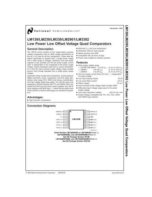
<strong>LM139</strong>/<strong>LM239</strong>/<strong>LM339</strong>/<strong>LM2901</strong>/<strong>LM3302</strong><strong>Low</strong> <strong>Power</strong> <strong>Low</strong> <strong>Offset</strong> Voltage Quad ComparatorsGeneral DescriptionThe <strong>LM139</strong> series consists of four independent precisionvoltage comparators with an offset voltage specification aslow as 2 mV max for all four comparators. These were designedspecifically to operate from a single power supplyover a wide range of voltages. Operation from split powersupplies is also possible and the low power supply currentdrain is independent of the magnitude of the power supplyvoltage. These comparators also have a unique characteristicin that the input common-mode voltage range includesground, even though operated from a single power supplyvoltage.Application areas include limit comparators, simple analog todigital converters; pulse, squarewave and time delay generators;wide range VCO; MOS clock timers; multivibratorsand high voltage digital logic gates. The <strong>LM139</strong> series wasdesigned to directly interface with TTL and CMOS. When operatedfrom both plus and minus power supplies, they will directlyinterface with MOS logic — where the low power drainof the <strong>LM339</strong> is a distinct advantage over standard comparators.Advantagesn High precision comparatorsConnection Diagramsn Reduced V OS drift over temperaturen Eliminates need for dual suppliesn Allows sensing near GNDn Compatible with all forms of logicn <strong>Power</strong> drain suitable for battery operationFeaturesn Wide supply voltage range— <strong>LM139</strong>/139A Series 2 to 36 V DC or ±1 to±18 V DC— <strong>LM2901</strong>: 2 to 36 V DC or ±1 to±18 V DC— <strong>LM3302</strong>: 2 to 28 V DC or ±1 to±14 V DCn Very low supply current drain (0.8 mA) — independentof supply voltagen <strong>Low</strong> input biasing current:25 nAn <strong>Low</strong> input offset current:±5 nAn <strong>Offset</strong> voltage:±3 mVn Input common-mode voltage range includes GNDn Differential input voltage range equal to the powersupply voltagen <strong>Low</strong> output saturation voltage: 250 mV at 4 mAn Output voltage compatible with TTL, DTL, ECL, MOSand CMOS logic systemsDS005706-27Order Number <strong>LM139</strong>AW/883 or <strong>LM139</strong>W/883 (Note 1)<strong>LM139</strong>AWRQML and <strong>LM139</strong>AWRQMLV(Note 3)See NS Package Number W14B<strong>LM139</strong>AWGRQML and <strong>LM139</strong>AWGRQMLV(Note 3)See NS Package Number WG14ANovember 1999<strong>LM139</strong>/<strong>LM239</strong>/<strong>LM339</strong>/<strong>LM2901</strong>/<strong>LM3302</strong> <strong>Low</strong> <strong>Power</strong> <strong>Low</strong> <strong>Offset</strong> Voltage Quad Comparators© 1999 National Semiconductor Corporation DS005706 www.national.com
<strong>LM139</strong>/<strong>LM239</strong>/<strong>LM339</strong>/<strong>LM2901</strong>/<strong>LM3302</strong>Typical Performance Characteristics <strong>LM139</strong>/<strong>LM239</strong>/<strong>LM339</strong>, <strong>LM139</strong>A/<strong>LM239</strong>A/<strong>LM339</strong>A, <strong>LM3302</strong>Supply CurrentInput CurrentOutput Saturation VoltageDS005706-34DS005706-35DS005706-36Response Time for VariousInput Overdrives — NegativeTransitionResponse Time for VariousInput Overdrives — PositiveTransitionDS005706-37DS005706-38Typical Performance Characteristics <strong>LM2901</strong>Supply CurrentInput CurrentOutput Saturation VoltageDS005706-39DS005706-40DS005706-41www.national.com 6
Typical Performance Characteristics <strong>LM2901</strong> (Continued)Response Time for VariousInput Overdrives — NegativeTransitionResponse Time for VariousInput Overdrives-PositiveTransition<strong>LM139</strong>/<strong>LM239</strong>/<strong>LM339</strong>/<strong>LM2901</strong>/<strong>LM3302</strong>Application HintsDS005706-42The <strong>LM139</strong> series are high gain, wide bandwidth deviceswhich, like most comparators, can easily oscillate if the outputlead is inadvertently allowed to capacitively couple to theinputs via stray capacitance. This shows up only during theoutput voltage transition intervals as the comparatorchanges states. <strong>Power</strong> supply bypassing is not required tosolve this problem. Standard PC board layout is helpful as itreduces stray input-output coupling. Reducing this input resistorsto < 10 kΩ reduces the feedback signal levels and finally,adding even a small amount (1 to 10 mV) of positivefeedback (hysteresis) causes such a rapid transition that oscillationsdue to stray feedback are not possible. Simplysocketing the IC and attaching resistors to the pins will causeinput-output oscillations during the small transition intervalsunless hysteresis is used. If the input signal is a pulse waveform,with relatively fast rise and fall times, hysteresis is notrequired.All pins of any unused comparators should be tied to thenegative supply.The bias network of the <strong>LM139</strong> series establishes a draincurrent which is independent of the magnitude of the powersupply voltage over the range of from 2 V DC to 30 V DC .It is usually unnecessary to use a bypass capacitor acrossthe power supply line.DS005706-43The differential input voltage may be larger than V + withoutdamaging the device. Protection should be provided to preventthe input voltages from going negative more than −0.3V DC (at 25˚C). An input clamp diode can be used as shownin the applications section.The output of the <strong>LM139</strong> series is the uncommitted collectorof a grounded-emitter NPN output transistor. Many collectorscan be tied together to provide an output OR’ing function. Anoutput pull-up resistor can be connected to any availablepower supply voltage within the permitted supply voltagerange and there is no restriction on this voltage due to themagnitude of the voltage which is applied to the V + terminalof the <strong>LM139</strong>A package. The output can also be used as asimple SPST switch to ground (when a pull-up resistor is notused). The amount of current which the output device cansink is limited by the drive available (which is independent ofV + ) and the β of this device. When the maximum current limitis reached (approximately 16 mA), the output transistor willcome out of saturation and the output voltage will rise veryrapidly. The output saturation voltage is limited by the approximately60Ω R SAT of the output transistor. The low offsetvoltage of the output transistor (1 mV) allows the output toclamp essentially to ground level for small load currents.Typical Applications (V + = 5.0 V DC )Basic ComparatorDriving CMOSDriving TTLDS005706-3DS005706-4DS005706-57www.national.com
<strong>LM139</strong>/<strong>LM239</strong>/<strong>LM339</strong>/<strong>LM2901</strong>/<strong>LM3302</strong>Typical Applications (V + = 5.0 V DC ) (Continued)AND GateOR GateDS005706-8DS005706-9Typical Applications (V + = 15 V DC )One-Shot MultivibratorDS005706-10Bi-Stable MultivibratorDS005706-11www.national.com 8
Typical Applications (V + = 15 V DC ) (Continued)One-Shot Multivibrator with Input Lock Out<strong>LM139</strong>/<strong>LM239</strong>/<strong>LM339</strong>/<strong>LM2901</strong>/<strong>LM3302</strong>DS005706-129www.national.com
<strong>LM139</strong>/<strong>LM239</strong>/<strong>LM339</strong>/<strong>LM2901</strong>/<strong>LM3302</strong>Typical Applications (V + = 15 V DC ) (Continued)Large Fan-In AND GateORing the OutputsDS005706-13DS005706-15www.national.com 10
Typical Applications (V + = 15 V DC ) (Continued)Pulse Generator<strong>LM139</strong>/<strong>LM239</strong>/<strong>LM339</strong>/<strong>LM2901</strong>/<strong>LM3302</strong>DS005706-1711www.national.com
<strong>LM139</strong>/<strong>LM239</strong>/<strong>LM339</strong>/<strong>LM2901</strong>/<strong>LM3302</strong>Typical Applications (V + = 15 V DC ) (Continued)Time Delay GeneratorDS005706-14Non-Inverting Comparator with HysteresisInverting Comparator with HysteresisDS005706-18DS005706-19www.national.com 12
Typical Applications (V + = 15 V DC ) (Continued)Squarewave OscillatorBasic ComparatorDS005706-21<strong>LM139</strong>/<strong>LM239</strong>/<strong>LM339</strong>/<strong>LM2901</strong>/<strong>LM3302</strong>DS005706-16Limit ComparatorComparing Input Voltagesof Opposite PolarityDS005706-20DS005706-2413www.national.com
<strong>LM139</strong>/<strong>LM239</strong>/<strong>LM339</strong>/<strong>LM2901</strong>/<strong>LM3302</strong>Typical Applications (V + = 15 V DC ) (Continued)Output StrobingDS005706-22* Or open-collector logic gate without pull-up resistorCrystal Controlled OscillatorDS005706-25www.national.com 14
Typical Applications (V + = 15 V DC ) (Continued)DS005706-23<strong>LM139</strong>/<strong>LM239</strong>/<strong>LM339</strong>/<strong>LM2901</strong>/<strong>LM3302</strong>V + =+30 V DC250 mV DC ≤V C ≤+50 V DC700 Hz≤f o ≤100 kHzTwo-Decade High-Frequency VCO15www.national.com
<strong>LM139</strong>/<strong>LM239</strong>/<strong>LM339</strong>/<strong>LM2901</strong>/<strong>LM3302</strong>Typical Applications (V + = 15 V DC ) (Continued)Transducer AmplifierZero Crossing Detector (Single <strong>Power</strong> Supply)DS005706-28DS005706-30Split-Supply Applications (V + =+15 V DC and V − =−15 V DC )MOS Clock DriverDS005706-31www.national.com 16
Split-Supply Applications (V + =+15 V DC and V − =−15 V DC ) (Continued)Zero Crossing DetectorComparator With a NegativeReference<strong>LM139</strong>/<strong>LM239</strong>/<strong>LM339</strong>/<strong>LM2901</strong>/<strong>LM3302</strong>DS005706-32Schematic DiagramDS005706-33DS005706-117www.national.com
Physical Dimensions inches (millimeters) unless otherwise noted (Continued)<strong>LM139</strong>/<strong>LM239</strong>/<strong>LM339</strong>/<strong>LM2901</strong>/<strong>LM3302</strong>Molded Dual-In-Line Package (N)Order Number <strong>LM339</strong>N, <strong>LM339</strong>AN, <strong>LM2901</strong>N or <strong>LM3302</strong>NNS Package Number N14AOrder Number <strong>LM139</strong>AW/883 or <strong>LM139</strong>W/883NS Package Number W14B19www.national.com
<strong>LM139</strong>/<strong>LM239</strong>/<strong>LM339</strong>/<strong>LM2901</strong>/<strong>LM3302</strong> <strong>Low</strong> <strong>Power</strong> <strong>Low</strong> <strong>Offset</strong> Voltage Quad ComparatorsNotesLIFE SUPPORT POLICYNATIONAL’S PRODUCTS ARE NOT AUTHORIZED FOR USE AS CRITICAL COMPONENTS IN LIFE SUPPORTDEVICES OR SYSTEMS WITHOUT THE EXPRESS WRITTEN APPROVAL OF THE PRESIDENT AND GENERALCOUNSEL OF NATIONAL SEMICONDUCTOR CORPORATION. As used herein:1. Life support devices or systems are devices orsystems which, (a) are intended for surgical implantinto the body, or (b) support or sustain life, andwhose failure to perform when properly used inaccordance with instructions for use provided in thelabeling, can be reasonably expected to result in asignificant injury to the user.National SemiconductorCorporationAmericasTel: 1-800-272-9959Fax: 1-800-737-7018Email: support@nsc.comwww.national.comNational SemiconductorEuropeFax: +49 (0) 1 80-530 85 86Email: europe.support@nsc.comDeutsch Tel: +49 (0) 1 80-530 85 85English Tel: +49 (0) 1 80-532 78 32Français Tel: +49 (0) 1 80-532 93 58Italiano Tel: +49 (0) 1 80-534 16 802. A critical component is any component of a lifesupport device or system whose failure to performcan be reasonably expected to cause the failure ofthe life support device or system, or to affect itssafety or effectiveness.National SemiconductorAsia Pacific CustomerResponse GroupTel: 65-2544466Fax: 65-2504466Email: sea.support@nsc.comNational SemiconductorJapan Ltd.Tel: 81-3-5639-7560Fax: 81-3-5639-7507National does not assume any responsibility for use of any circuitry described, no circuit patent licenses are implied and National reserves the right at any time without notice to change said circuitry and specifications.