

A PMOSFET ESD Failure Caused by Localized Charge - Stanford ...
A PMOSFET ESD Failure Caused by Localized Charge - Stanford ...
A PMOSFET ESD Failure Caused by Localized Charge - Stanford ...

You also want an ePaper? Increase the reach of your titles
YUMPU automatically turns print PDFs into web optimized ePapers that Google loves.
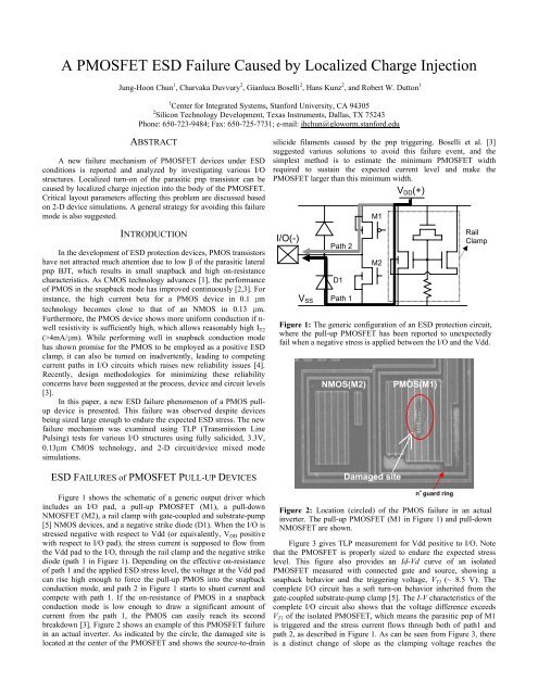
A <strong>PMOSFET</strong> <strong>ESD</strong> <strong>Failure</strong> <strong>Caused</strong> <strong>by</strong> <strong>Localized</strong> <strong>Charge</strong> InjectionJung-Hoon Chun 1 , Charvaka Duvvury 2 , Gianluca Boselli 2 , Hans Kunz 2 , and Robert W. Dutton 11 Center for Integrated Systems, <strong>Stanford</strong> University, CA 943052 Silicon Technology Development, Texas Instruments, Dallas, TX 75243Phone: 650-723-9484; Fax: 650-725-7731; e-mail: jhchun@gloworm.stanford.eduABSTRACTA new failure mechanism of <strong>PMOSFET</strong> devices under <strong>ESD</strong>conditions is reported and analyzed <strong>by</strong> investigating various I/Ostructures. <strong>Localized</strong> turn-on of the parasitic pnp transistor can becaused <strong>by</strong> localized charge injection into the body of the <strong>PMOSFET</strong>.Critical layout parameters affecting this problem are discussed basedon 2-D device simulations. A general strategy for avoiding this failuremode is also suggested.INTRODUCTIONIn the development of <strong>ESD</strong> protection devices, PMOS transistorshave not attracted much attention due to low β of the parasitic lateralpnp BJT, which results in small snapback and high on-resistancecharacteristics. As CMOS technology advances [1], the performanceof PMOS in the snapback mode has improved continuously [2,3]. Forinstance, the high current beta for a PMOS device in 0.1 µmtechnology becomes close to that of an NMOS in 0.13 µm.Furthermore, the PMOS device shows more uniform conduction if n-well resistivity is sufficiently high, which allows reasonably high I T2(>4mA/µm). While performing well in snapback conduction modehas shown promise for the PMOS to be employed as a positive <strong>ESD</strong>clamp, it can also be turned on inadvertently, leading to competingcurrent paths in I/O circuits which raises new reliability issues [4].Recently, design methodologies for minimizing these reliabilityconcerns have been suggested at the process, device and circuit levels[3].In this paper, a new <strong>ESD</strong> failure phenomenon of a PMOS pullupdevice is presented. This failure was observed despite devicesbeing sized large enough to endure the expected <strong>ESD</strong> stress. The newfailure mechanism was examined using TLP (Transmission LinePulsing) tests for various I/O structures using fully salicided, 3.3V,0.13µm CMOS technology, and 2-D circuit/device mixed modesimulations.<strong>ESD</strong> FAILURES of <strong>PMOSFET</strong> PULL-UP DEVICESFigure 1 shows the schematic of a generic output driver whichincludes an I/O pad, a pull-up <strong>PMOSFET</strong> (M1), a pull-downNMOSFET (M2), a rail clamp with gate-coupled and substrate-pump[5] NMOS devices, and a negative strike diode (D1). When the I/O isstressed negative with respect to Vdd (or equivalently, V DD positivewith respect to I/O pad), the stress current is supposed to flow fromthe Vdd pad to the I/O, through the rail clamp and the negative strikediode (path 1 in Figure 1). Depending on the effective on-resistanceof path 1 and the applied <strong>ESD</strong> stress level, the voltage at the Vdd padcan rise high enough to force the pull-up PMOS into the snapbackconduction mode, and path 2 in Figure 1 starts to shunt current andcompete with path 1. If the on-resistance of PMOS in a snapbackconduction mode is low enough to draw a significant amount ofcurrent from the path 1, the PMOS can easily reach its secondbreakdown [3]. Figure 2 shows an example of this <strong>PMOSFET</strong> failurein an actual inverter. As indicated <strong>by</strong> the circle, the damaged site islocated at the center of the <strong>PMOSFET</strong> and shows the source-to-drainsilicide filaments caused <strong>by</strong> the pnp triggering. Boselli et al. [3]suggested various solutions to avoid this failure event, and thesimplest method is to estimate the minimum <strong>PMOSFET</strong> widthrequired to sustain the expected current level and make the<strong>PMOSFET</strong> larger than this minimum width.V DD (+)I/O(-)Path 2D1V SS Path 1Figure 1: The generic configuration of an <strong>ESD</strong> protection circuit,where the pull-up <strong>PMOSFET</strong> has been reported to unexpectedlyfail when a negative stress is applied between the I/O and the Vdd.NMOS(M2)M1M2Damaged sitePMOS(M1)n + guard ringRailClampFigure 2: Location (circled) of the PMOS failure in an actualinverter. The pull-up <strong>PMOSFET</strong> (M1 in Figure 1) and pull-downNMOSFET are shown.Figure 3 gives TLP measurement for Vdd positive to I/O. Notethat the <strong>PMOSFET</strong> is properly sized to endure the expected stresslevel. This figure also provides an Id-Vd curve of an isolated<strong>PMOSFET</strong> measured with connected gate and source, showing asnapback behavior and the triggering voltage, V T1 (~ 8.5 V). Thecomplete I/O circuit has a soft turn-on behavior inherited from thegate-coupled substrate-pump clamp [5]. The I-V characteristics of thecomplete I/O circuit also shows that the voltage difference exceedsV T1 of the isolated <strong>PMOSFET</strong>, which means the parasitic pnp of M1is triggered and the stress current flows through both of path1 andpath 2, as described in Figure 1. As can be seen from Figure 3, thereis a distinct change of slope as the clamping voltage reaches the
triggering voltage of the PMOS, leading to a decreased on-resistance.In this I/O circuit, a large amount of current (> 2.5 A) can besustained even after the stress voltage exceeds the V T1 , since the<strong>PMOSFET</strong> is sized large enough to endure this level of <strong>ESD</strong> stress. Itis also worth pointing out that the <strong>ESD</strong> damage was observed in therail clamp, not in the <strong>PMOSFET</strong> (M1).Current [A]1.61.41.21.00.80.60.40.2I/O(-)Figure 3: IV curves generated <strong>by</strong> TLP tests of an output drivercircuit and an isolated PMOS transistor. A large current (> 2.5 A)can be sustained <strong>by</strong> the output driver even after the stress voltageexceeds the V T1. There is a distinct change of slope at I = 0.65Awhere the parasitic pnp transistor is triggered on.n +(guardring)VDD(+)RailClampI/O(-)0.00.00 2 4 6 8 10Voltage [V]PMOS(M1)PMOS(M1)V DD (+)Parasitic pnptriggeredn + guard ringp + n + /n -(V SS ) (I/O pad)V T11.61.41.21.00.80.60.40.2Current [mA/µm]Figure 4: An example of PMOS failure in an actual I/O circuit.PMOS (M1 in Figure 1) devices are located in two differentblocks. A negative strike diode (D1 in Figure 1) which consists ofp+ (Vss) and n+/n- (I/O pad) is at the rightmost side. Between thetwo PMOS blocks and at the right side of the lower PMOS block,there are n+ diffusion lines connected to the guard ring. An <strong>ESD</strong>damaged site (the circled region) is observed close to the negativestrike diode.However, although the <strong>PMOSFET</strong> is sized large enough toendure the required stress level, we consistently encountered the<strong>PMOSFET</strong> <strong>ESD</strong> damage phenomenon in certain I/O circuits. Thepattern of this behavior is quite different from that of the typical<strong>PMOSFET</strong> failure described in Figure 2. Figure 4 shows an exampleof new <strong>PMOSFET</strong> failure patterns. This specific I/O has a complexguard ring shape with a short n + stripe at the right side of the lower<strong>PMOSFET</strong> block and another n + stripe between the two <strong>PMOSFET</strong>blocks. The two vertical stripes at the rightmost side are p+ diffusion(connected to Vss) and n+/n-well diffusion (connected to I/O pad),forming a negative strike diode (D1 in Figure 1). It should be notedthat the <strong>ESD</strong> damaged site with molten drain/source contacts [6, 7] isobserved close to the negative strike diode but not at the center as inFigure 2. This failure pattern appeared consistently in certain I/Ocircuits with failing at 2.2 kV HBM condition even though they aredesigned to endure more than 5 kV. This fact indicates that there is asystematic effect which lowers <strong>ESD</strong> immunity level.Current [A]1.51.00.5I/O AI/O BI/O C0.00 1 2 3 4 5 6 7 8 9 10I T2Voltage [V]Figure 5: Measured IV curves of various I/O structures up tofailure points, generated <strong>by</strong> TLP tests.Table 1: The layout information and <strong>ESD</strong> test results of variousI/O circuits. DR1 is the distance between the negative strike diodeand the guard ring (see the representation of layouts in Figure 6).DR1 n + guard ring HBM Fail LevelI/O A 0.8 µm Incomplete 2.2 kVI/O B 0.8 µm Incomplete 2.4 kVI/O C > 0.8 µm Incomplete 2.9 kVI/O D 1.0 µm Incomplete 3.4 kVI/O E 22 µm complete > 5 kVFigure 5 shows TLP IV curves of three different I/O circuitswhich have similar failure patterns displayed in Figure 4. The designparameters and I T2 (translated to HBM failure level) of each deviceare listed in Table 1. In Table 1, DR1 is the distance between thenegative strike diode and the guard ring, as illustrated in thesimplified layout diagrams of Figure 6. While the I T2 of I/O E (ofwhich the measured I-V curve is shown in Figure 3) is higher than 2.5A (~5kV HBM), I/O A and B fail even before the voltage reaches V T1of an isolated <strong>PMOSFET</strong> and show the HBM level lower than 2.5 kV.All device dimensions such as the width of <strong>PMOSFET</strong>s and powerclamps are almost identical, whereas their layouts have somevariations in the guard ring shape and the distance between thenegative strike diode and the guard ring (named as DR1) etc. Forexample, DR1 of I/O E is larger than 22 µm, but I/O A, B have 0.8µm DR1. In I/O C, the PMOS block is not located parallel to thediode, and the shortest path from the diode to the guard ring aroundthe PMOS block is about 0.8 µm long. The guard ring of I/O E iscompletely closed as in Figure 2, while in other I/O circuits the oneside of the guard ring does not have metal contacts (see Figure 6b inthe next section).
Two observed facts should be emphasized here; first thedamaged spots of I/O A,B,C and D are always located in the PMOStransistor near the negative strike diode as can be seen in Figure 4.Second, when DR1 increases from 0.8 µm to 1.0 µm the <strong>ESD</strong> failurelevel increases <strong>by</strong> about 1 kV. These TLP test results show that thedistance between the negative strike diode and the guard ring(DR1),and the shape of the guard ring can be critical parameters determining<strong>ESD</strong> immunity of I/O circuits. The physics involved in thisphenomenon will be clarified in the next section.ANALYSIS OF A NEW FAILURE MECHANISMIn Figure 6, schematics of the I/O layout are illustrated forfacilitating the following discussions. The location of the <strong>ESD</strong>damaged spot is indicated in each schematic. The p-substrate to n-well diode (D1) are located adjacent to PMOS pull-up devices (M1),and <strong>ESD</strong> damage occurs in the vicinity of the diode and around thecenter of gate fingers. The distance from p + V SS to n + guard ring isnoted as DR1, and the distance between p + V SS and n + diffusionconnected to I/O is DR2. The guard ring shown in Figure 6a hasmetal contacts at every closure, but in Figure 6b one stripe betweenthe PMOS and the diode does not have a metal contact in order toachieve a more compact design. The influence of this difference inthe guard ring shape will be discussed in detail in the next section.Damaged regionn + Guard Ringp + /V SS n + / I/O padinternal avalanche generation of carriers (I AV ) [8]. Here R well_1 , R well_2and R GR act as effective body resistance of the <strong>PMOSFET</strong>. However,if these two devices are moved closer, the analysis with D1 in Figure7 is no longer valid and the parasitic npn BJT (T2 in the dotted box ofFigure 7) should be considered instead of D1; this npn transistorsupplies the external triggering current (I inject ) to the base of pnptransistor. This explanation can be clarified <strong>by</strong> the simulation resultsshown in Figure 8.I <strong>ESD</strong>Figure 7: Schematic of the equivalent circuit under <strong>ESD</strong>conditions. The parasitic npn BJT in the dotted box (T 2 ) should beconsidered only if a negative strike diode is placed close to thepull-up <strong>PMOSFET</strong> (M1).I/O (-)I/O (-)VDD (+)RailClampM 1I BI diodeD 1T 1R GR + R well_2R well_1I injectT 2VDD (+)I clamPMOSPULL-UP(M1)D1R_Well_1N-WellSTIR_Well_2R_GRDR1Rail ClampP-Sub(a)DR1DR2I/O (-)VDD (+)(a)Damaged region No ContactPMOSPULL-UP(M1)x(b)DR1 DR2ActiveN-wellContactPolyFigure 6: Simplified diagrams of I/O layout. Only PMOS pull-updevices(M1 in Figure 1) and negative strike diodes(D1 in Figure1) are illustrated. a) Its guard ring has metal contacts at everyclosure, b) metal contacts are missing at one stripe.Figure 7 shows the schematic of the equivalent circuit of an I/Ocircuit under <strong>ESD</strong> conditions, which includes the devices involved inboth path 1 and path 2 of Figure 1. Here, R well_1 and R well_2 representthe resistance of n-well from source/n-well junction to the n+ guardring (see also Figure 8a). R GR is the extra resistance caused <strong>by</strong>incomplete contact formation as illustrated in Figure 6b. If the diodeD1 is far from the pull-up PMOS device and decoupled from eachother, path 1 and path 2 can be analyzed independently. In this case,the parasitic pnp BJT (T1) is triggered through self-biasing using theyR GRD1N-WellP-SubSTIR_GR(b)electroninjectionRail ClampFigure 8: Current Flow lines under <strong>ESD</strong> conditions. a) The PMOStransistor is separated away from the negative strike diode (DR1 =3 µm), b) the PMOS is close to the diode, therefore the twodevices are electrically coupled (DR1 = 1 µm).In order to investigate the influence of each layout parametervariations, circuit/device mixed mode simulations were performed.The device structure and external circuit components employed in thesimulation are illustrated in Figure 8. The rail clamp in Figure 8 isimplemented with a constant resistance, R clamp , since the on-resistanceof rail clamps can be considered constant in a wide high-current range[3]. The value of R clamp is extracted from the measurement resultswhen parasitic pnp transistors are triggered. This figure also showsthe simulated current flowlines of I/O devices represented <strong>by</strong> theequivalent circuit of Figure 7. In Figure 8a, the negative strike diodeis located distantly from the n + guard ring (DR1 ≈ 3 µm), thereforemost of the electrons emitted through n-well/substrate junction fromthe I/O pad recombine with the holes from V SS which is connected to
the rail clamp. However, if the two devices are located close to eachother (DR1 ≈ 1 µm), some portion of electrons from the diode areinjected into the n-well body of the <strong>PMOSFET</strong>, modulating the basepotential of the pnp transistor (T1 in Figure 7). This process results inearly turn-on of the parasitic pnp transistor. If R GR increases as in thecase of Figure 6b, the base potential is further modulated due to thevoltage drop across the R GR , resulting in lower triggering voltage.These simulation results and the analysis of the equivalentcircuit in Figure 7 explain the cause of the PMOS failure reported inthe previous section. The structure of Figure 6b has severaldrawbacks compared to the guard ring structure of Figure 6a. First,due to the smaller distance from the diode, the body potential of<strong>PMOSFET</strong> (the base potential of the pnp transistor) is modulated <strong>by</strong>the current injected from the diode. Second, incomplete guard ringmetal causes spatial variations of the effective body resistance, whichis reflected in R GR of the equivalent circuit. These two drawbackscause the non-uniform turn on of pnp transistors and degrade <strong>ESD</strong>immunity of I/O circuits.INFLUENCE OF LAYOUT PARAMETER VARIATIONSConsidering that the BJT is a current controlled device, we canformulate the triggering voltage for the case that the PMOS and thenegative strike diode are electrically coupled, with reference to theequivalent circuit of Figure 7.I inject = Iclamp⋅ β(eq. 1)V DD _ Pontential = Iclamp⋅ Rclamp+ Vdiode=1βI inject ⋅ ⋅ Rclamp+V body trig ≈ ( RGR+ Rwell_ 2 ⋅ ( IAV− IB+ Iinject,, ) trigVdiode)(eq. 2)+ Rwell_1⋅(IAV− IB)(eq. 3)Here, β is the common emitter current gain of the npn transistor(in the dotted box of Figure 7). I inject is the electron current from thenegative strike diode into n-well of the PMOS transistor, and it isassumed that most of this electron current flows directly to the guardring contacts through R well2 as shown in the current flowlines ofFigure 8. V diode is the voltage drop through the negative strike diodeand is a function of DR2 in Figure 6. I inject, trig is I inject at the pnptriggering point. V body, trig is the body potential near the source/bodyjunction with reference to V DD at the triggering point, and can beconsidered as constant. In equation 3, I inject, trig is much larger than I AVif the PMOS and the diode are located in proximity to each other, andthen equation 2 can be approximated as follows.VDD _ Potential @ pnp triggering=VT1≈VRGR+ Rbody,trigwell _ 21⋅ ⋅ Rβclamp+ Vdiode(eq. 4)As DR1 decreases, the common emitter current gain (β) ofparasitic npn increases, hence V T1 decreases as expected in equation 4.As can be seen in Figure 9, the triggering point of parasitic pnp of the<strong>PMOSFET</strong> is a strong function of DR1. For instance, when DR1 isreduced from 1.2 µm to 1.0 µm, V T1 decreases <strong>by</strong> ~ 1 V. The devicewith 0.8 µm DR1 is triggered around 5.7 V, without showingsnapback behavior. However, if DR1 is larger than 1.2 µm, V T1 is notsensitive to DR1 variation. In other words, the localized electroninjection from the negative strike diode into the body of <strong>PMOSFET</strong>sincreases significantly if DR1 is less than a certain value, and causesnon-uniform conduction along the x-direction in Figure 6, thereforedeteriorating the <strong>ESD</strong> robustness of I/O circuitsCurrent [A]0.200.150.100.05DR1 = 0.8µmDR1 = 1.0µmDR1 = 1.2µm0.000 1 2 3 4 5 6 7 8 910.10.01<strong>PMOSFET</strong> V DS[V]Figure 9: Simulated Id-Vd characteristics of PMOS transistor inI/O circuits with various distances between the guard ring andnegative diode. DR1 lower than 1.2 µm considerably affects thetriggering voltage of pnp transistors. Here, R GR is 0 Ohm and DR2is 0.6 µm.I B, I C[A]DR1=0.8µmDR1=1.0µmDR1=1.2µmDR1=1.5µmDR1=2.0µm1.0 1.5 2.0V BE[V]Figure 10: Simulated collector and base currents of the parasiticnpn transistor (T2 in Figure 7) as functions of the emitter-basevoltage with various distances between the negative strike diodeand guard ring (DR1).β, (I C/I B)0.40.30.20.10.01.4 1.6 1.8 2.0V BE[V]I BI CDR1=0.8µmDR1=1.0µmDR1=1.2µmDR1=1.5µmDR1=2.0µmFigure 11: Simulated current gains as functions of emitter-basevoltage with various distances between the negative strike diodeand guard ring (DR1).
In order to investigate the effect of DR1 variations on thecharacteristics of the parasitic npn transistor, collector current (I C ,same as I inject ), base current (I B , same as I clamp ) and the static commonemittercurrent gain, β are plotted in Figure 10 and Figure 11. Sincethe doping concentration of the emitter (n-well) is not much higherthan that of the base (p-substrate), emitter efficiency (γ) is muchsmaller than 1. If DR1 is larger than 1.5 µm, the base transport factor(α T ) is much less than unity, therefore β is less than 0.1. However,the peak β increases over 0.1 as DR1 decreases to 1.2 µm, and a largecurrent is injected into the body of <strong>PMOSFET</strong>, causing early turn-onof the pnp transistor.U-shape guard ring shows considerable variation of the spreadingR well , which may cause non-uniform conduction along both x and ydirections.xy(x,y)=(0,0)A+-(0,-7.5)Current [A]0.200.150.100.050.00DR2 = 0.4 µmDR2 = 0.6 µmDR2 = 0.8 µmDR2 = 1.0 µmDR2 = 1.2 µm5 6 7 8 9<strong>PMOSFET</strong> V DSVoltage [V]Figure 12: Simulated Id-Vd characteristics of PMOS transistor inI/O circuits with various distances between the p+ diffusion andn+ diffusion of the negative diode (DR2). Here, R GR is 0 Ohm andDR1 is 1.0 µmFigure 12 shows that as the DR2 (the distance between p+ VSSand n+ diffusion connected to I/O pad) increases, the triggeringvoltage also increases, due to the decrease of T2’s β and the increaseof V diode in equation 4. However this also causes the on-resistance ofpath 1 in Figure 1 to be increased, therefore increasing DR2 is not anefficient solution to mitigate the stress on the PMOS in path 2.In the mixed mode simulations, a lumped resistor, R GR isemployed in order to reflect the finite conductivity of n+ diffusionlayer of guard ring (see Figure 6b). However, all segmented devicesare connected also through the n-well as well as through n+ diffusions,therefore the spreading resistance should be calculated for extractingan effective R GR . As shown in Figure 13, 3-dimensional simulationswere performed for calculating the distributed well resistance andinvestigating the effect of guard ring structure variation on the wellresistance. In Figure 13, two guard ring structures are shown; the oneis the closed guard ring as in Figure 6a and the other is the U-typeguard ring in which one stripe does not have metal contacts but hasonly n+ diffusion as in Figure 6b. In each structure, a contact islocated inside the guard ring closure for injecting electron currentwhich flows to the guard ring. By measuring the voltage differencebetween this contact and the guard ring, we can extract effective R wellfrom a certain location inside the guard ring closure to the guard ring.Figure 14 shows R well variations in two guard ring structures along theline A-A’ (close to the negative strike diode) of Figure 13b. Theextracted resistance values are normalized with reference to the valueat the middle of A-A’. At the location away from the center of A-A’<strong>by</strong> 3 µm, the R well of the U-type guard ring structure decreases <strong>by</strong>~7 %, while the variation of R well inside the closed guard ring is lessthan 1 %. The variation of R well along the line B-B’ is also plotted inFigure 15. As shown in Figure 14 and Figure 15, the device with anFigure 13: Extraction of spreading well resistance (R well ) (a)closed guard ring as in Figure 6a, and (b) U-shape guard ring as inFigure 6b.Rwell(-6.2,y) / Rwell(-6.2,0)1.21.00.815 µm (-7.5,0)15 µmB’Guard Ring MetalN-wellP-sub(a)A(b)Contact for <strong>Charge</strong>InjectionClosed GRU-shape GR0.6AA'-8 -6 -4 -2 0 2 4 6 8Distance from the Center, y [µm]Figure 14: Variations of the spreading well resistance along y-direction near guarding (x = - 6.2 µm, along the line A-A’). Thespreading well resistance is normalized with reference to the valueat the center.A+B-A’
Rwell(x,0) / Rwell(0,0)1.41.21.00.80.6BClosed GRU-shape GR-6 -4 -2 0 2 4 6Distance from the Center, x [µm]Figure 15: Variations of the spreading well resistance along x-direction (y = 0 µm, along the line B-B’). The spreading wellresistance is normalized with reference to the value at the center.For thorough investigation of the effect of this R well variation on<strong>ESD</strong> immunity, 3-D <strong>ESD</strong> simulations with various guard ringstructures should be performed. However, in this work the effect ofR well variation is investigated with 2-D simulation <strong>by</strong> simply varyingthe lumped resistance, R GR between V DD and the n+ guard ring. In 2-D simulation, the well resistance, R well0 (= R well1 +R well2 , of Figure 7)is extracted from I sub vs I d curve [8, 9] with zero R GR , and then acertain fraction of R well0 is applied to R GR . As expected from equation4, higher R GR causes the body potential of the <strong>PMOSFET</strong> to risehigher and the pnp transistor is triggered at lower V T1 . Figure 16shows that the triggering voltage with , R GR of 2% R well0 is lower thanthe triggering voltage with zero R GR <strong>by</strong> ~ 0.4 V. This observationimplies that the finite resistance of the n+ guard ring without a metalcontact results in non-uniform potential distributions across the bodyof PMOS transistors and the localized current conduction.Current [A]0.120.100.080.060.040.020.00Rgr = + 0 %Rgr = + 2 %Rgr = + 4 %Rgr = + 6 %B'5 6 7 8<strong>PMOSFET</strong> V DSVoltage [V]Figure 16: Id-Vd characteristics of PMOS transistors in I/Ocircuits with various external resistance between the body contactand the V DD . DR1 and DR2 are 1.0 µm and 0.6 µm, respectively.DESIGN IMPACTThis paper demonstrates the layout of the PMOS relative todiffused regions connected to the I/O pin, can play a role in theeffectiveness of the overall protection at the pad. The best possibleoption is to move the PMOS layout more than 20 µm away from theI/O protection devices. However, in most cases this may not bepractical. In an ASIC environment various types of buffers would usethe same protection cell at the pad but the output NMOS and PMOSare laid out differently depending on the design features. Somebuffers might tolerate a series resistor between the I/O pad and thePMOS and in these cases the interference from the PMOS is notrelevant and the final protection level is determined <strong>by</strong> the currentlimited to the PMOS, or the failure current limit of the Vdd protectiondevice itself. However in common output buffer designs, a resistor isnot tolerated, along with the fact that the PMOS device sizes aredifferent depending on the designed buffer's performance. Forexample, a 4 mA buffer would have relatively larger PMOS than a 2mA buffer. However, if the layout is ineffective then the PMOS sizedoes not matter. Once the layout is made more effective as describedin this paper, then the PMOS size would play a role in determiningthe overall protection level. In this case, for <strong>ESD</strong> purposes it isdesirable to make the 2 mA buffer PMOS look like the 4 mA buffer.This may be achieved with the introduction of a dummy PMOS asmentioned in [3,4]. Of course the critical factor is thelayout. Specifically, in an ASIC library environment the placement ofthe protection devices and the latchup guard rings can be complex dueto the available macro pitch and the bus architecture. If the negativediode at the pad has to be placed in proximity to the PMOS then it isessential to completely close the guard ring around the PMOS withfull contacts and maintain DR1 in Figure 6 to be > 2 µm. If thisspacing can be >10 µm then the guard ring shape should not matter.CONCLUSIONSA new failure phenomenon of <strong>PMOSFET</strong> pull-up devices under<strong>ESD</strong> conditions has been reported and analyzed <strong>by</strong> investigatingvarious I/O structures of 3.3 V, 0.13µm CMOS technology. Thephysical mechanism and the influence of layout parameters such asthe distance between a negative strike diode and an n+ guardring(DR1), guard ring shape, and effective resistance of the rail clamp,were investigated through Transmission Line Pulse (TLP) testing anddevice/circuit mixed mode simulations.<strong>Localized</strong> turn-on of the parasitic pnp BJT of the <strong>PMOSFET</strong> pullupdevice can be caused <strong>by</strong> the localized charge injection into thebody of <strong>PMOSFET</strong> from the negative strike diode. The most criticallayout parameter regarding this failure is DR1. Values of DR1 greaterthan 2 µm are recommended for a safe design with the technologyused in this study. This phenomenon can be implicated in <strong>ESD</strong>failures of all future ASIC I/O circuits which require more compactlayouts.ACKNOWLEDGMENTSResearch support <strong>by</strong> Texas Instruments is gratefullyacknowledged. Jung-Hoon Chun is supported <strong>by</strong> Eric andIlleana Benhamou FellowshipREFERENCES[1] C.-H. Choi, “Modeling of Nanoscale MOSFETs,” PhD thesis,<strong>Stanford</strong> University, 2002.[2] R. A. Ashton and Y. Smooha, “Characterization of a 0.16µmCMOS Technology using SEMATECH <strong>ESD</strong> Benchmarking
Structures,” in Proceedings of 23 rd EOS/<strong>ESD</strong> Symposium,EOS/<strong>ESD</strong> 2001, Portland, OR, pp. 435-444.[3] G. Boselli, C. Duvvury, and V. Reddy, “Efficient pnpCharacteristics of PMOS Transistors in Sub-0.13µm <strong>ESD</strong>Protection Circuits,” in Proceedings of 24 rd EOS/<strong>ESD</strong>Symposium, EOS/<strong>ESD</strong> 2002.[4] L.-M. Ting, C. Duvvury, O. Trevino, J. Schichl. And T. Diep,“Integration of TLP analysis for <strong>ESD</strong> Troubleshooting”, inProceedings of 23 rd EOS/<strong>ESD</strong> Symposium, EOS/<strong>ESD</strong> 2001,Portland, OR, pp. 445-452.[5] C. Duvvury, S. Ramaswamy, A. Ameraskera, R. A. Cline, B. H.Andresen, and V. Gupta, “Substrate pump NMOS for <strong>ESD</strong>Protection Applications,” in Proceedings of 21 st EOS/<strong>ESD</strong>Symposium, EOS/<strong>ESD</strong> 1999, pp. 7-17.[6] K. Oh, J. Chun, K. Banerjee, C. Duvvury, and R. W. Dutton,“Modeling of Temperature Dependent Contact Resistance forAnalysis of <strong>ESD</strong> Reliability,” In Proceedings of InternationalReliability Physics Symposium 2003, pp. 226-234.[7] A. Ameraskera, V. Gupta, K. Vasanth, and S. Ramaswamy,“Analysis of snapback behavior on the <strong>ESD</strong> capability of sub-0.20 µm NMOS”, In Proceedings of International ReliabilityPhysics Symposium 1999, pp. 159-166[8] S. Ramaswamy, A. Amerasekera, and M. Chang “A unifiedsubstrate current model for weak and strong impact ionization insub-0.25micron NMOS devices”, Tech. Digest of IEDM 1997,pp. 885-888.[9] X. Zhang, “Modeling and characterization of substrate resistancefor deep submicron <strong>ESD</strong> protection devices,” PhD thesis,<strong>Stanford</strong> University, 2002.


