

On-Chip Inductance Modeling and RLC Extraction of VLSI - Stanford ...
On-Chip Inductance Modeling and RLC Extraction of VLSI - Stanford ...
On-Chip Inductance Modeling and RLC Extraction of VLSI - Stanford ...

Create successful ePaper yourself
Turn your PDF publications into a flip-book with our unique Google optimized e-Paper software.
<strong>On</strong>-<strong>Chip</strong> <strong>Inductance</strong> <strong>Modeling</strong> <strong>and</strong> <strong>RLC</strong> <strong>Extraction</strong> <strong>of</strong> <strong>VLSI</strong> Interconnects for Circuit<br />
Simulation<br />
Xiaoning Qi, Ga<strong>of</strong>eng Wang, Zhiping Yu <strong>and</strong> Robert W. Dutton<br />
Center for Integrated Systems, <strong>Stanford</strong> University, <strong>Stanford</strong>, CA 94305<br />
Tak Young<br />
Synopsys Inc. Mountain View, CA 94043<br />
Norman Chang<br />
Hewlett-Packard Laboratories, Palo Alto, CA 94303<br />
Abstract - <strong>On</strong>-<strong>Chip</strong> inductance modeling <strong>of</strong> <strong>VLSI</strong> interconnects<br />
is presented which captures 3D geometry from layout<br />
design <strong>and</strong> process technology information. Analytical formulae<br />
are derived for quick <strong>and</strong> accurate inductance estimation which<br />
can be used in circuit simulations <strong>and</strong> whole chip extraction<br />
screening process. Circuit simulations show critical global wire<br />
inductive effects as well as power <strong>and</strong> ground inductive noise.<br />
I. INTRODUCTION<br />
With high clock frequencies <strong>and</strong> faster transistor rise/fall<br />
time in modern <strong>VLSI</strong> circuits, long signal wires exhibit transmission<br />
line effects. Because <strong>of</strong> the use <strong>of</strong> wider wire <strong>and</strong> Cu<br />
interconnects for critical signals such as clock trees, inductance<br />
<strong>of</strong> the interconnect can no longer be ignored compared<br />
with its resistive component. Due to on-chip inductance<br />
effects, signal ringing is observed, cross talk is increased <strong>and</strong><br />
power/ground bounce (noise) becomes worse. In high clock<br />
frequency microprocessor <strong>and</strong> ASIC designs, clock trees <strong>and</strong><br />
power/ground grid need to be designed carefully to avoid<br />
large clock skew, signal inductive coupling <strong>and</strong> ground<br />
bounce [1][2].<br />
To accurately model on-chip inductance, 3D geometry<br />
modeling which is based on 2D geometry layout information<br />
<strong>and</strong> process technology information is required. Electromagnetic<br />
field solvers are typically used to extract inductance<br />
based on these 3D geometry modeling. The values are <strong>of</strong>ten<br />
used as golden results <strong>of</strong> inductance extraction. Since it is<br />
computational expensive to use field solvers for the whole<br />
chip extraction, analytical formulae are desired to quickly <strong>and</strong><br />
accurately calculate on-chip inductance. This is particularly<br />
important in the extraction screening process to identify<br />
inductively critical nets for further detailed analysis.<br />
In this paper, we present a fast <strong>and</strong> accurate 3D geometry<br />
modeling tool based on Arcadia [3] data base. Fasthenry [4] is<br />
used as field solver to extract on-chip inductance. Analytical<br />
formulae are derived for self <strong>and</strong> mutual inductance estimation.<br />
Accurate self inductances <strong>of</strong> wires are also calculated<br />
based on the self inductances <strong>and</strong> their mutual inductances <strong>of</strong><br />
the cascaded segments. Very good agreement <strong>of</strong> the calculation<br />
results from formulae with field solver simulation has<br />
been achieved. Circuit simulations <strong>of</strong> global wires with<br />
inductance extraction demonstrate inductive ringing effects<br />
<strong>and</strong> power/ground inductive noise.<br />
II. 3D GEOMETRY MODELING AND INDUCTANCE EXTRACTION<br />
USING FIELD SOLVER<br />
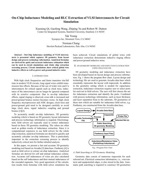
3D geometry modeling <strong>and</strong> inductance extraction have<br />
been developed based on layout design <strong>and</strong> process information.<br />
Fig. 1 shows the program flow chart. Layout design <strong>and</strong><br />
technology file are used to generate Arcadia data base which<br />
essentially represents the layout with trapezoids. In addition<br />
to the geometry setting which is needed for capacitance<br />
extraction, inductance extraction requires user to select ports<br />
for each net in field solvers. The user will first choose the net<br />
for inductance extraction <strong>and</strong> identify the ports. Combined<br />
with process technology information, such as layer thickness<br />
<strong>and</strong> layer separation from to the substrate, 3D geometries <strong>of</strong><br />
these nets which are suitable for inductance field solver, e.g.<br />
Fasthenry, are constructed from the Arcadia data base.<br />
Layout Design<br />
Arcadia Technology<br />
File<br />
Arcadia Data Base<br />
Process<br />
trapezoids<br />
Paths Searching<br />
3D geometry <strong>Modeling</strong><br />
Fasthenry Input Files<br />
<strong>Inductance</strong>/Resistance Value<br />
(Partial/loop <strong>Inductance</strong>)<br />
Fig. 1 Program Flow Chart<br />
Probe File<br />
Selected Net (s)<br />
A. Path Searching in 3D Geometry <strong>Modeling</strong><br />
Geometry data consist <strong>of</strong> numerous trapezoids for each<br />
selected net. Electrical connection information, i.e., vias/contacts<br />
<strong>and</strong> equipotential edges, is also stored in the data. Automatic<br />
path searching is required to construct 3D geometries
<strong>of</strong> the selected nets since each net usually includes many<br />
branches. The data structure is designed to facilitate the<br />
searching process which is a depth-first searching. Fig. 2<br />
shows a search process to find a net which has ports <strong>of</strong> segment<br />
1 <strong>and</strong> segment 10. Algorithm identifies the trapezoids<br />
where they are located. Then it starts with segment 1, <strong>and</strong><br />
does depth-first search <strong>and</strong> constructs a tree as shown in Fig.<br />
2. If the segment is the destination port <strong>of</strong> the net, the program<br />
stops; otherwise, it continues searching on another<br />
branch. This process continues until the second port is found.<br />
To build the whole path, algorithm traces back (dashed<br />
arrows) to complete the path construction.<br />
1 2 0<br />
Multi-nets/ports can be processed together in order to find<br />
the mutual inductances <strong>of</strong> different nets.<br />
B. <strong>Inductance</strong> <strong>Extraction</strong><br />
3 4 0<br />
5 6 0 7 8 0<br />
0 9 10 0<br />
0<br />
Fig. 2 Path searching in 3D geometry modeling.<br />
The program generates input files for field solvers such as<br />
Fasthenry for inductance extraction. Because <strong>of</strong> proximity<br />
effects in high frequencies, a window enclosing the extracted<br />
nets can be defined which is bounded by nearest power/<br />
ground lines. Current returns <strong>of</strong> the nets are assumed to be<br />
through these power/ground lines. Therefore, loop inductance<br />
as well as partial inductance can be extracted. For example, a<br />
wire <strong>of</strong> length <strong>of</strong> about 2.82 mm <strong>and</strong> width <strong>of</strong> 1.2 µm in a<br />
commercial chip has partial inductance 4.67 nH <strong>and</strong> loop<br />
inductance 5.7 nH (ground line width <strong>of</strong> 8 µm). The mutual<br />
inductance (loop) with one <strong>of</strong> its neighbor line is 2.26 nH.<br />
III. ANALYTICAL FORMULAE FOR INDUCTANCE ESTIMATION<br />
Field solver extraction <strong>of</strong> inductance has high accuracy but<br />
it is time <strong>and</strong> memory expensive. It might not be practical for<br />
a whole chip inductance extraction. However, the extracted<br />
inductance value can be used as golden data for quick inductance<br />
estimation. To quickly calculate on-chip inductance for<br />
design guidance as well as for screening inductive important<br />
nets in the whole chip, analytical formulae are desired. In this<br />
section, self inductance as well as mutual inductance formulae<br />
are investigated <strong>and</strong> derived. Simulation results <strong>and</strong> analytical<br />
formulae estimations are in very good agreement.<br />
A. Self <strong>Inductance</strong> Formula <strong>and</strong> Mutual <strong>Inductance</strong> Formula<br />
for Two Parallel Wire with Equal Length<br />
Self inductance <strong>of</strong> a wire with rectangular cross section can<br />
be derived using electromagnetic field theory <strong>and</strong> geometry<br />
mean distance (G.M.D.)[5]. Equation (1) is for the self inductance<br />
when l » ( w+<br />
t)<br />
where l is the length <strong>of</strong> the wires. w<br />
<strong>and</strong> t are the width <strong>and</strong> thickness <strong>of</strong> the rectangular cross section,<br />
respectively. Equation (2) is for the mutual inductance <strong>of</strong><br />
two parallel wires <strong>of</strong> distance d <strong>and</strong> equal length l when l > d,<br />
µ<br />
L self<br />
----- 0<br />
l<br />
(1)<br />
2π<br />
ln 2l<br />
-----------<br />
⎝<br />
⎛ w+<br />
t⎠<br />
⎞ l<br />
=<br />
+ -- + 0.2235( w+<br />
t)<br />
2<br />
M<br />
µ 0<br />
-------<br />
l ⎛2l<br />
---- ⎞ d<br />
= ln – 1 + -- (2)<br />
2π ⎝d<br />
⎠ l<br />
The self inductance is a nonlinear function <strong>of</strong> l which<br />
means it is non-scalable with respect to length. It is superlinear<br />
when l > ( w+<br />
t)<br />
.<br />
To consider skin effect, special frequency dependent term<br />
needs to be added. This term can be represented by Bessel<br />
function [5] which is curve fitted as shown in Fig. 3 where δ<br />
is the skin depth at a particular frequency. Fig. 4 plots the<br />
comparison between the simulation <strong>and</strong> formulae with <strong>and</strong><br />
without skin effect. The revised formula accurately captures<br />
the skin effect though the frequency dependency is not large.<br />
Skin effect Term X<br />
0.4<br />
0.3<br />
0.2<br />
0.1<br />
δ<br />
x = ---------------------------------<br />
0.2235( w + t)<br />
X=0.4372x if x < 0.5<br />
X=0.0578x+0.1897if 0.5 ≤ x ≤1<br />
X=0.25 if x > 1<br />
0<br />
0 1 2 3 4 5<br />
skinDepth/equivalent radius (x)<br />
Fig. 3 Skin effect term. δ is the skin depth.<br />
µ l 0<br />
L -------- self 2π<br />
ln 2l<br />
-----------<br />
⎝<br />
⎛ w + t⎠<br />
⎞ 1 0.2235( w+<br />
t)<br />
=<br />
+ -- + --------------------------------- – µ ( 0.25 – X)<br />
2 l r<br />
1.19<br />
w = 8µm t = 1µm l = 1mm<br />
1.185<br />
<strong>Inductance</strong> (nH)<br />
1.18<br />
1.175<br />
1.17<br />
1.165<br />
Simulations<br />
Formula with skin effect<br />
Formula without skin effect<br />
1.16<br />
0 2 4 6 8 10<br />
Frequency (GHz)<br />
Fig. 4 Revised formula with the skin effect term.<br />
error: 0.27%
B. Mutual <strong>Inductance</strong> <strong>of</strong> Two Parallel Wires with Unequal<br />
Length.<br />
To calculate wire inductance in a complex wire environment<br />
or self inductance consisting <strong>of</strong> several cascaded segments<br />
in sequence, mutual inductance formulae <strong>of</strong> two<br />
parallel wires with unequal length are derived. There are six<br />
different positions <strong>of</strong> two parallel wires which result in six<br />
mutual inductance formulae. Fig. 5 illustrates the six different<br />
cases. l, m, p, q <strong>and</strong> s represent the wire lengths <strong>and</strong> some<br />
wire overlap lengths. d is the wires distance.<br />
l<br />
d<br />
d<br />
p<br />
m<br />
s<br />
Case 1<br />
Case 3<br />
l<br />
m<br />
d<br />
l<br />
m<br />
q<br />
l<br />
d<br />
Fig. 5 Six relative positions for mutual inductance.<br />
If the wave length <strong>of</strong> the signal at frequencies <strong>of</strong> interest is<br />
much larger than the dimension <strong>of</strong> the wire, the magnetic<br />
induction at every point <strong>of</strong> the field is in phase with the current.<br />
The induced electromotive forces are at all points in<br />
phase. The magnetic flux linked with a wire may be considered<br />
as the resultant <strong>of</strong> the fluxes (which is in phase under<br />
quasi-stationary condition) contributed by the separate elements<br />
<strong>of</strong> the inducing circuit. That is, the mutual inductance<br />
<strong>of</strong> a wire with the inducing wires is the algebraic sum <strong>of</strong> the<br />
mutual inductances <strong>of</strong> the separate elements <strong>of</strong> the inducing<br />
wires. For example, the mutual inductance <strong>of</strong> the two wires in<br />
the case 3 can be calculated as,<br />
M =<br />
1 2 -- [( M m+ p + M m + q ) – ( M p + M q )]<br />
where M m+p represents the mutual inductance <strong>of</strong> the two<br />
parallel wires with m+p equal length <strong>and</strong> separation <strong>of</strong> d. So<br />
are the other mutual terms.<br />
Six formulae like (3) can be obtained <strong>and</strong> six formulae can<br />
be derived based on (2). For example, for Case 4, it can be<br />
shown as,<br />
M 1 µ 0<br />
(4)<br />
2 -- ----- l ⎛ l<br />
----------- ⎞<br />
⎛4m( l–<br />
m)<br />
⎞<br />
= ln + mln<br />
2π ⎝l<br />
– m⎠<br />
⎜------------------------<br />
d 2 ⎟ – 2m + d<br />
⎝ ⎠<br />
where l, m <strong>and</strong> d are as indicated in Fig. 5.<br />
Fig. 6 shows the comparison <strong>of</strong> the model based on (4)<br />
with the field solver simulations. As seen, the formula gives<br />
d<br />
m<br />
m<br />
s<br />
Case 2<br />
l<br />
m<br />
Case 4<br />
Case 5 Case 6<br />
s<br />
l<br />
(3)<br />
accurate estimations for reasonable distance. When distance<br />
become comparable to wire length, analytical formulae will<br />
underestimate the mutual inductance. For on-chip interconnects,<br />
wires usually are thin <strong>and</strong> long compared to their separation<br />
in the simulation window. Therefore, it does not result<br />
in appreciable errors. Case 1 <strong>and</strong> Case 6 share same formula<br />
<strong>and</strong> their mutual inductances usually are negligible because<br />
the magnetic flux linked each other in each case is very small.<br />
<strong>Inductance</strong> (nH)<br />
0.8<br />
0.7<br />
0.6<br />
0.5<br />
0.4<br />
0.3<br />
0.2<br />
0.1<br />
Case 4:<br />
1mm<br />
0.5mm<br />
w=5 µm<br />
t=1 µm<br />
Simulation<br />
Formula<br />
0<br />
0 100 200 300 400 500<br />
Distance <strong>of</strong> the lines (µm)<br />
Fig. 6 Formula <strong>and</strong> simulation comparison.<br />
Case 2:<br />
u 0 l + m – s<br />
M ----- ( l – s)<br />
⎛-------------------<br />
⎞ ( l + m–<br />
s)<br />
⎛4s( m–<br />
s)<br />
⎞<br />
= ln + m ln------------------------<br />
+ s ln ----------------------<br />
4π ⎝ l – s ⎠<br />
⎜<br />
m–<br />
s ⎝ d 2 ⎟ – 2s<br />
⎠<br />
Case 3:<br />
u 0<br />
M ----- m 4( m + p)<br />
( m+<br />
q)<br />
( m + p)<br />
( m+<br />
q)<br />
= ln----------------------------------------<br />
4π<br />
d 2 + p ln------------------<br />
+ q ln-----------------<br />
– 2m<br />
p<br />
q<br />
Case 5:<br />
u 0<br />
M ----- l ⎛l<br />
+ m<br />
-----------⎞<br />
( l + m)<br />
= ln + m ln----------------<br />
– d<br />
4π ⎝ l ⎠ m<br />
Case 1 & 6:<br />
u 0<br />
M ----- ( l + s)<br />
⎛l + m + s<br />
-------------------- ⎞ ( l + m + s)<br />
s<br />
= ln + m ln-------------------------<br />
+ s ------------<br />
4π ⎝ l + s ⎠ m + s<br />
ln ⎝<br />
⎛ m+<br />
s⎠<br />
⎞<br />
Fig. 7 Other mutual inductance formulae.<br />
C. Calculation <strong>of</strong> self <strong>Inductance</strong> <strong>of</strong> a Whole Wire<br />
As indicated in section A, if a wire consists <strong>of</strong> several segments<br />
<strong>of</strong> which self inductances are known, the whole wire’s<br />
self inductance does not equal to the sum <strong>of</strong> all the self inductances<br />
<strong>of</strong> all the segments because <strong>of</strong> the existence <strong>of</strong> mutual<br />
inductances. Instead, all segments’ self inductances as well as<br />
mutual inductances between these segments are required to<br />
compute the whole wire’s self inductance. It can be shown,<br />
using circuit theory, that the self inductance <strong>of</strong> a whole wire<br />
constructed by cascaded segments is as,<br />
N N N<br />
L self<br />
= ∑ l i<br />
+ ∑ ∑ 2k ij<br />
M ij (5)<br />
i = 1 i = 1 j = i+<br />
1<br />
where N is the number <strong>of</strong> segments. l i is the self inductance
<strong>of</strong> segment i. M i,j is the mutual inductance between segment i<br />
<strong>and</strong> j <strong>of</strong> the whole wire. k ij = 0 when segment i <strong>and</strong> j are<br />
orthogonal; k ij = 1 when i <strong>and</strong> j have same current direction;<br />
k ij = – 1 when i <strong>and</strong> j have opposite current direction. Table<br />
1 shows three typical wire structures’ inductance calculation<br />
<strong>and</strong> their field solver simulations results.<br />
TABLE ISimulation <strong>and</strong> calculation <strong>of</strong> self inductance. (nH)<br />
Wire1: 3 segments <strong>and</strong><br />
3 turns (1.8 mm)<br />
Wire2: 4 segments <strong>and</strong><br />
4 turns (2.1 mm)<br />
IV. APPLICATION OF INDUCTANCE CALCULATION IN CIRCUIT<br />
SIMULATION<br />
For on-chip long thin wires, self inductance <strong>of</strong> a wire is<br />
solely determined by wire geometry, <strong>and</strong> mutual inductance<br />
<strong>of</strong> two wires is solely determined by geometries <strong>of</strong> the two<br />
wires <strong>and</strong> their spacing [6]. Therefore, the formulae developed<br />
above can be used to calculate self/mutual inductance<br />
for <strong>RLC</strong> interconnect modeling <strong>and</strong> circuit simulations to<br />
investigate inductive effects as well as power/ground noise.<br />
Self inductance <strong>of</strong> global wires, power line <strong>and</strong> ground line<br />
<strong>and</strong> mutual inductance between these lines can be calculated<br />
using the derived formulae. Capacitance <strong>and</strong> resistance can<br />
also be quickly calculated. Fig.8 shows one global wire (4<br />
mm long <strong>and</strong> 5 µm wide) <strong>and</strong> two nearest power/ground lines<br />
(10 µm wide) within a selected window. Fig. 9 shows the simulation<br />
<strong>of</strong> the signal at the output <strong>of</strong> the receiver <strong>of</strong> the global<br />
wire. The overshoots are clearly observed with inductance<br />
effect included. Fig.10 shows the power noise <strong>and</strong> ground<br />
bounce when power/ground inductive effects are included in<br />
circuit simulation. Measures must be taken to avoid circuit<br />
failure, such as moving global wire closer to ground/power<br />
lines <strong>and</strong> using C4 bumps for power/ground lines.<br />
V. CONCULSIONS<br />
Wire3: 5 segments <strong>and</strong><br />
5 turns (4mm)<br />
Sim. Cal. Error Sim. Cal. Error Sim. Cal. Error<br />
2.27 2.26 0.4% 2.93 2.86 2.3% 5.35 5.17 3.4%<br />
20 µm<br />
Power<br />
Ground<br />
signal<br />
3000 µm<br />
2000 µm<br />
4000 µm<br />
200µm<br />
200µm<br />
2000 µm<br />
1000 µm<br />
Fig. 8 <strong>On</strong>e global line <strong>and</strong> two power/ground lines.<br />
20 µm<br />
220 µm<br />
<strong>On</strong>-chip inductance modeling <strong>of</strong> interconnects is presented<br />
which is based on accurate automatic 3D geometry generation.<br />
Analytical formulae derived for self <strong>and</strong> mutual inductance<br />
estimation are benchmarked with simulations, suitable<br />
Voltage (V)<br />
Fig. 9 Signal wave forms at the output <strong>of</strong> receiver: ringing effects with <strong>RLC</strong><br />
simulation.<br />
Voltage (V)<br />
4<br />
3<br />
2<br />
1<br />
0<br />
-1<br />
4<br />
3<br />
2<br />
1<br />
0<br />
Input to the driver<br />
Output signal (<strong>RLC</strong> sim.)<br />
Output signal (RC sim.)<br />
0 0.5 1 1.5 2<br />
Time (ns)<br />
Fig. 10 Power <strong>and</strong> ground noise observed with <strong>RLC</strong> simulation.<br />
for quick inductance extraction. Extracted <strong>RLC</strong> used in circuit<br />
simulation shows impact <strong>of</strong> on-chip inductance on signal<br />
integrity <strong>and</strong> power/ground noise.<br />
ACKNOWLEDGMENT<br />
Authors would like to thank Arcadia R&D group at Synopsys<br />
Inc. The project is supported by Focus Center Research<br />
Program for Interconnects for Gigascale Integration. Contract<br />
No. B-12-D00-S5.<br />
REFERENCES<br />
VDD = 3.3v<br />
Power voltage change at the receiver<br />
Ground voltage change at the receiver<br />
GND = 0v<br />
-10 0.5 1 1.5 2<br />
Time (ns)<br />
[1] P. J. Restle, “High speed interconnects: a designers perspective”,<br />
ICCAD’98 Tutorial: Interconnect in high speed designs: problems,<br />
methodologies <strong>and</strong> tools, Nov. 1998.<br />
[2] B. Klevel<strong>and</strong>, X. Qi, L. Madden, R. Dutton <strong>and</strong> S. Wong, “Line inductance<br />
extraction <strong>and</strong> modeling in a real chip with power grid”, IEDM’99.<br />
Dec. 1999.<br />
[3] Arcadia User Manual, Synopsys Corp.<br />
[4] M. Kamon, M.J. Tsuk, <strong>and</strong> J. White, “FASTHENRY: a multipole accelerated<br />
3D inductance extraction program”, IEEE Trans. Microwave Theory<br />
& Techniques, pp. 1750, 1994.<br />
[5] E. B. Rosa <strong>and</strong> F. W. Grover, “Formulas <strong>and</strong> tables for the calculation <strong>of</strong><br />
mutual <strong>and</strong> self-inductance”, Government Printing Office, 1916.<br />
[6] L. He, N. Chang, S. Lin <strong>and</strong> O.S. Nakagawa, “Efficient inductance modeling<br />
for on-chip interconnects”, IEEE CICC’99, pp. 457,1999.


