

On-Chip Inductance Modeling and RLC Extraction of VLSI - Stanford ...
On-Chip Inductance Modeling and RLC Extraction of VLSI - Stanford ...
On-Chip Inductance Modeling and RLC Extraction of VLSI - Stanford ...

You also want an ePaper? Increase the reach of your titles
YUMPU automatically turns print PDFs into web optimized ePapers that Google loves.
<strong>of</strong> segment i. M i,j is the mutual inductance between segment i<br />
<strong>and</strong> j <strong>of</strong> the whole wire. k ij = 0 when segment i <strong>and</strong> j are<br />
orthogonal; k ij = 1 when i <strong>and</strong> j have same current direction;<br />
k ij = – 1 when i <strong>and</strong> j have opposite current direction. Table<br />
1 shows three typical wire structures’ inductance calculation<br />
<strong>and</strong> their field solver simulations results.<br />
TABLE ISimulation <strong>and</strong> calculation <strong>of</strong> self inductance. (nH)<br />
Wire1: 3 segments <strong>and</strong><br />
3 turns (1.8 mm)<br />
Wire2: 4 segments <strong>and</strong><br />
4 turns (2.1 mm)<br />
IV. APPLICATION OF INDUCTANCE CALCULATION IN CIRCUIT<br />
SIMULATION<br />
For on-chip long thin wires, self inductance <strong>of</strong> a wire is<br />
solely determined by wire geometry, <strong>and</strong> mutual inductance<br />
<strong>of</strong> two wires is solely determined by geometries <strong>of</strong> the two<br />
wires <strong>and</strong> their spacing [6]. Therefore, the formulae developed<br />
above can be used to calculate self/mutual inductance<br />
for <strong>RLC</strong> interconnect modeling <strong>and</strong> circuit simulations to<br />
investigate inductive effects as well as power/ground noise.<br />
Self inductance <strong>of</strong> global wires, power line <strong>and</strong> ground line<br />
<strong>and</strong> mutual inductance between these lines can be calculated<br />
using the derived formulae. Capacitance <strong>and</strong> resistance can<br />
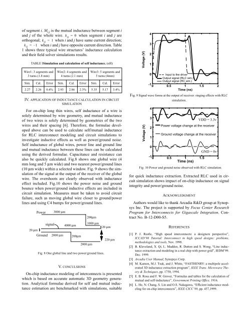
also be quickly calculated. Fig.8 shows one global wire (4<br />
mm long <strong>and</strong> 5 µm wide) <strong>and</strong> two nearest power/ground lines<br />
(10 µm wide) within a selected window. Fig. 9 shows the simulation<br />
<strong>of</strong> the signal at the output <strong>of</strong> the receiver <strong>of</strong> the global<br />
wire. The overshoots are clearly observed with inductance<br />
effect included. Fig.10 shows the power noise <strong>and</strong> ground<br />
bounce when power/ground inductive effects are included in<br />
circuit simulation. Measures must be taken to avoid circuit<br />
failure, such as moving global wire closer to ground/power<br />
lines <strong>and</strong> using C4 bumps for power/ground lines.<br />
V. CONCULSIONS<br />
Wire3: 5 segments <strong>and</strong><br />
5 turns (4mm)<br />
Sim. Cal. Error Sim. Cal. Error Sim. Cal. Error<br />
2.27 2.26 0.4% 2.93 2.86 2.3% 5.35 5.17 3.4%<br />
20 µm<br />
Power<br />
Ground<br />
signal<br />
3000 µm<br />
2000 µm<br />
4000 µm<br />
200µm<br />
200µm<br />
2000 µm<br />
1000 µm<br />
Fig. 8 <strong>On</strong>e global line <strong>and</strong> two power/ground lines.<br />
20 µm<br />
220 µm<br />
<strong>On</strong>-chip inductance modeling <strong>of</strong> interconnects is presented<br />
which is based on accurate automatic 3D geometry generation.<br />
Analytical formulae derived for self <strong>and</strong> mutual inductance<br />
estimation are benchmarked with simulations, suitable<br />
Voltage (V)<br />
Fig. 9 Signal wave forms at the output <strong>of</strong> receiver: ringing effects with <strong>RLC</strong><br />
simulation.<br />
Voltage (V)<br />
4<br />
3<br />
2<br />
1<br />
0<br />
-1<br />
4<br />
3<br />
2<br />
1<br />
0<br />
Input to the driver<br />
Output signal (<strong>RLC</strong> sim.)<br />
Output signal (RC sim.)<br />
0 0.5 1 1.5 2<br />
Time (ns)<br />
Fig. 10 Power <strong>and</strong> ground noise observed with <strong>RLC</strong> simulation.<br />
for quick inductance extraction. Extracted <strong>RLC</strong> used in circuit<br />
simulation shows impact <strong>of</strong> on-chip inductance on signal<br />
integrity <strong>and</strong> power/ground noise.<br />
ACKNOWLEDGMENT<br />
Authors would like to thank Arcadia R&D group at Synopsys<br />
Inc. The project is supported by Focus Center Research<br />
Program for Interconnects for Gigascale Integration. Contract<br />
No. B-12-D00-S5.<br />
REFERENCES<br />
VDD = 3.3v<br />
Power voltage change at the receiver<br />
Ground voltage change at the receiver<br />
GND = 0v<br />
-10 0.5 1 1.5 2<br />
Time (ns)<br />
[1] P. J. Restle, “High speed interconnects: a designers perspective”,<br />
ICCAD’98 Tutorial: Interconnect in high speed designs: problems,<br />
methodologies <strong>and</strong> tools, Nov. 1998.<br />
[2] B. Klevel<strong>and</strong>, X. Qi, L. Madden, R. Dutton <strong>and</strong> S. Wong, “Line inductance<br />
extraction <strong>and</strong> modeling in a real chip with power grid”, IEDM’99.<br />
Dec. 1999.<br />
[3] Arcadia User Manual, Synopsys Corp.<br />
[4] M. Kamon, M.J. Tsuk, <strong>and</strong> J. White, “FASTHENRY: a multipole accelerated<br />
3D inductance extraction program”, IEEE Trans. Microwave Theory<br />
& Techniques, pp. 1750, 1994.<br />
[5] E. B. Rosa <strong>and</strong> F. W. Grover, “Formulas <strong>and</strong> tables for the calculation <strong>of</strong><br />
mutual <strong>and</strong> self-inductance”, Government Printing Office, 1916.<br />
[6] L. He, N. Chang, S. Lin <strong>and</strong> O.S. Nakagawa, “Efficient inductance modeling<br />
for on-chip interconnects”, IEEE CICC’99, pp. 457,1999.


