

On-Chip Inductance Modeling and RLC Extraction of VLSI - Stanford ...
On-Chip Inductance Modeling and RLC Extraction of VLSI - Stanford ...
On-Chip Inductance Modeling and RLC Extraction of VLSI - Stanford ...

Create successful ePaper yourself
Turn your PDF publications into a flip-book with our unique Google optimized e-Paper software.
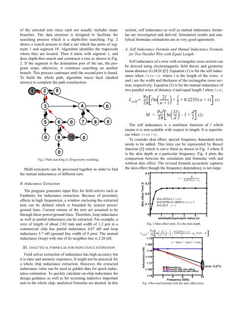
<strong>of</strong> the selected nets since each net usually includes many<br />
branches. The data structure is designed to facilitate the<br />
searching process which is a depth-first searching. Fig. 2<br />
shows a search process to find a net which has ports <strong>of</strong> segment<br />
1 <strong>and</strong> segment 10. Algorithm identifies the trapezoids<br />
where they are located. Then it starts with segment 1, <strong>and</strong><br />
does depth-first search <strong>and</strong> constructs a tree as shown in Fig.<br />
2. If the segment is the destination port <strong>of</strong> the net, the program<br />
stops; otherwise, it continues searching on another<br />
branch. This process continues until the second port is found.<br />
To build the whole path, algorithm traces back (dashed<br />
arrows) to complete the path construction.<br />
1 2 0<br />
Multi-nets/ports can be processed together in order to find<br />
the mutual inductances <strong>of</strong> different nets.<br />
B. <strong>Inductance</strong> <strong>Extraction</strong><br />
3 4 0<br />
5 6 0 7 8 0<br />
0 9 10 0<br />
0<br />
Fig. 2 Path searching in 3D geometry modeling.<br />
The program generates input files for field solvers such as<br />
Fasthenry for inductance extraction. Because <strong>of</strong> proximity<br />
effects in high frequencies, a window enclosing the extracted<br />
nets can be defined which is bounded by nearest power/<br />
ground lines. Current returns <strong>of</strong> the nets are assumed to be<br />
through these power/ground lines. Therefore, loop inductance<br />
as well as partial inductance can be extracted. For example, a<br />
wire <strong>of</strong> length <strong>of</strong> about 2.82 mm <strong>and</strong> width <strong>of</strong> 1.2 µm in a<br />
commercial chip has partial inductance 4.67 nH <strong>and</strong> loop<br />
inductance 5.7 nH (ground line width <strong>of</strong> 8 µm). The mutual<br />
inductance (loop) with one <strong>of</strong> its neighbor line is 2.26 nH.<br />
III. ANALYTICAL FORMULAE FOR INDUCTANCE ESTIMATION<br />
Field solver extraction <strong>of</strong> inductance has high accuracy but<br />
it is time <strong>and</strong> memory expensive. It might not be practical for<br />
a whole chip inductance extraction. However, the extracted<br />
inductance value can be used as golden data for quick inductance<br />
estimation. To quickly calculate on-chip inductance for<br />
design guidance as well as for screening inductive important<br />
nets in the whole chip, analytical formulae are desired. In this<br />
section, self inductance as well as mutual inductance formulae<br />
are investigated <strong>and</strong> derived. Simulation results <strong>and</strong> analytical<br />
formulae estimations are in very good agreement.<br />
A. Self <strong>Inductance</strong> Formula <strong>and</strong> Mutual <strong>Inductance</strong> Formula<br />
for Two Parallel Wire with Equal Length<br />
Self inductance <strong>of</strong> a wire with rectangular cross section can<br />
be derived using electromagnetic field theory <strong>and</strong> geometry<br />
mean distance (G.M.D.)[5]. Equation (1) is for the self inductance<br />
when l » ( w+<br />
t)<br />
where l is the length <strong>of</strong> the wires. w<br />
<strong>and</strong> t are the width <strong>and</strong> thickness <strong>of</strong> the rectangular cross section,<br />
respectively. Equation (2) is for the mutual inductance <strong>of</strong><br />
two parallel wires <strong>of</strong> distance d <strong>and</strong> equal length l when l > d,<br />
µ<br />
L self<br />
----- 0<br />
l<br />
(1)<br />
2π<br />
ln 2l<br />
-----------<br />
⎝<br />
⎛ w+<br />
t⎠<br />
⎞ l<br />
=<br />
+ -- + 0.2235( w+<br />
t)<br />
2<br />
M<br />
µ 0<br />
-------<br />
l ⎛2l<br />
---- ⎞ d<br />
= ln – 1 + -- (2)<br />
2π ⎝d<br />
⎠ l<br />
The self inductance is a nonlinear function <strong>of</strong> l which<br />
means it is non-scalable with respect to length. It is superlinear<br />
when l > ( w+<br />
t)<br />
.<br />
To consider skin effect, special frequency dependent term<br />
needs to be added. This term can be represented by Bessel<br />
function [5] which is curve fitted as shown in Fig. 3 where δ<br />
is the skin depth at a particular frequency. Fig. 4 plots the<br />
comparison between the simulation <strong>and</strong> formulae with <strong>and</strong><br />
without skin effect. The revised formula accurately captures<br />
the skin effect though the frequency dependency is not large.<br />
Skin effect Term X<br />
0.4<br />
0.3<br />
0.2<br />
0.1<br />
δ<br />
x = ---------------------------------<br />
0.2235( w + t)<br />
X=0.4372x if x < 0.5<br />
X=0.0578x+0.1897if 0.5 ≤ x ≤1<br />
X=0.25 if x > 1<br />
0<br />
0 1 2 3 4 5<br />
skinDepth/equivalent radius (x)<br />
Fig. 3 Skin effect term. δ is the skin depth.<br />
µ l 0<br />
L -------- self 2π<br />
ln 2l<br />
-----------<br />
⎝<br />
⎛ w + t⎠<br />
⎞ 1 0.2235( w+<br />
t)<br />
=<br />
+ -- + --------------------------------- – µ ( 0.25 – X)<br />
2 l r<br />
1.19<br />
w = 8µm t = 1µm l = 1mm<br />
1.185<br />
<strong>Inductance</strong> (nH)<br />
1.18<br />
1.175<br />
1.17<br />
1.165<br />
Simulations<br />
Formula with skin effect<br />
Formula without skin effect<br />
1.16<br />
0 2 4 6 8 10<br />
Frequency (GHz)<br />
Fig. 4 Revised formula with the skin effect term.<br />
error: 0.27%


