Transistor amplifiers aet 8 - NCATT
Transistor amplifiers aet 8 - NCATT
Transistor amplifiers aet 8 - NCATT
- No tags were found...

You also want an ePaper? Increase the reach of your titles
YUMPU automatically turns print PDFs into web optimized ePapers that Google loves.
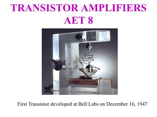
TRANSISTOR AMPLIFIERSAET 8First <strong>Transistor</strong> developed at Bell Labs on December 16, 1947
TRANSISTOR AMPLIFIERSObjective 1aIdentify Bipolar <strong>Transistor</strong> Amplifier OperatingPrinciples
TRANSISTOR AMPLIFIERSOverview(1) Dynamic Operation(2) Configurations(3) Common Emitter(4) Common Collector(5) Common Base(6) Temperature Stabilization(7) Coupling
TRANSISTOR AMPLIFIERSTypical Amplifier(A). Output taken from A toB:Reduce the resistance of R2,voltage from A to Bdecreases.Increase the resistance ofR2, voltage from A to Bincreases.(Voltage follows resistance)!
TRANSISTOR AMPLIFIERSTypical AmplifierResistor (R2) is replaced withtransistor (Q1)(B). Output taken from A to B:Reduce the resistance of Q1,voltage from A to Bdecreases.Increase the resistance of Q1,voltage from A to B increases.(Voltage follows resistance)!
TRANSISTOR AMPLIFIERSTypical Amplifier(C)An input signal from G1 isapplied to the basethrough C C . The inputsignal changes the Bias onthe base of the transistorcontrolling the current flowthrough the transistor.The output, taken from A toB, will be a reproduction ofthe input signal only muchlarger.
TRANSISTOR AMPLIFIERSCONFIGURATIONS
TRANSISTOR AMPLIFIERSCommon EmitterCommon Emitter issometimes called theGrounded Emitter.Input signal is appliedto the base.Output signal is takenfrom the collector.The common line,(not used for signal)is connected to theemitter.
TRANSISTOR AMPLIFIERSCommon CollectorCommon Collector (CC)is sometimes calledGrounded Collector.The input signal isapplied to the base.The output signal istaken from the emitter.The common line, (notused for signal) isconnected to thecollector.
TRANSISTOR AMPLIFIERSCommon BaseCommon Base (CB) issometimes calledGrounded Base.The input signal isapplied to the emitter.The output signal istaken from thecollector.The common line, (notused for signal) isconnected to the base.
TRANSISTOR AMPLIFIERSCommon Emitter AmplifierThe purpose of the commonemitter amplifier is to providegood current, voltage, andpower gain.180° phase shift
TRANSISTOR AMPLIFIERSCommon Emitter Amplifier ComponentsR 1 determinesforward biasR 2 aids indeveloping biasR 3 is the collectorload resistor used todevelop the outputsignalR 4 is the emitterresistor used forthermal stability
TRANSISTOR AMPLIFIERSCommon Emitter Amplifier ComponentsQ 1 - transistorC 1 is the inputcoupling capacitor
TRANSISTOR AMPLIFIERSCommon Emitter AmplifierCurrent paths andpercentage of flowI E = 100%, I C = 95%,I B = 5%NPN – Current flowsfrom Ground to +VCC
TRANSISTOR AMPLIFIERSCommon Emitter AmplifierSignal path: When a signal is applied toan amplifier, four things occur.Base, emitter & collector currentschange at the rate of the input signalCollector voltage changes at the rate ofthe input signalPhase shift of 180There will be signal gain!
TRANSISTOR AMPLIFIERSCommon Emitter AmplifierStatic or Quiescent OperationBy definition, bias is defined as theaverage DC voltage (or current)used to establish the operatingpoint in transistor circuits for astatic or quiescent condition. Astatic condition means the circuitdoes not have an input signal and isfixed in a non-varying condition.
TRANSISTOR AMPLIFIERSTypical Amplifier with Bias - Static Condition<strong>Transistor</strong> CurrentPath600mv (.6v) Bias(emitter to basevoltage) causesemitter current (IE),base current (IB),and collectorcurrent (IC) to flow.
TRANSISTOR AMPLIFIERSTypical Amplifier with Bias - Static ConditionCurrent enters theemitter and exitsthe base.Current enters theemitter and exitsthe collectorthrough R1 to V CC .
TRANSISTOR AMPLIFIERSCommon Emitter AmplifierDynamic OperationThe varying condition of a circuit iscalled its dynamic condition oroperating condition. This occurswhenever an input signal is applied.
TRANSISTOR AMPLIFIERSTypical Amplifier with Bias - DynamicDynamic condition: DC Bias with signal added(Varying condition)The output voltage has a much larger voltagechange than the input.
TRANSISTOR AMPLIFIERSTypical Amplifier with Bias - DynamicNotice the .2V Pk-Pk signal at the input is using the.6v DC as its reference and the output 10V Pk-Pksignal is using the 15V DC as its reference.
TRANSISTOR AMPLIFIERSCommon Emitter Amplifier
TRANSISTOR AMPLIFIERSNPN Common Emitter Amplifier OperationThe negative alternation of the input signalapplied to the base of the transistor causesforward bias to decrease and collectorcurrent to decrease.The voltage drop across R 3 decreasesbecause I C decreasedThe collector voltage (V C ) increasesThe bias decrease caused an increase inoutput voltage and produced a 180 phaseinversion
TRANSISTOR AMPLIFIERSNPN Common Emitter Amplifier OperationThe positive alternation of the input signalapplied to the base causes forward bias toincrease and collector current to increaseThe voltage drop across R 3 increasesbecause I C increasedThe collector voltage (V C ) decreasesThe bias increase caused a decrease inoutput voltage and produced a 180 phaseinversion
TRANSISTOR AMPLIFIERSCommon Emitter Amplifier
TRANSISTOR AMPLIFIERSCommon Emitter AmplifierNPN with conventionalpower connectionV CC to base andcollector usingrespective resistors(R 1 & R 2 ).
TRANSISTOR AMPLIFIERSCommon Emitter AmplifierNPN with alternatepower connection V EEto emitter withcurrent path throughQ 1 out the base andcollector through R 1& R 2 to ground.
TRANSISTOR AMPLIFIERSCommon Emitter AmplifierPNP with conventionalpower connection-V CC to base andcollector usingrespective resistors(R 1 & R 2 ).
TRANSISTOR AMPLIFIERSCommon Emitter AmplifierPNP with alternatepower connection+V EE to emitter withcurrent path in thebase and collectorthrough R 1 & R 2 outthe emitter toground.
TRANSISTOR AMPLIFIERSCommon Emitter AmplifierCharacteristic Curve GraphA transistor CHARACTERISTIC CURVE is agraph plotting of the relationshipsbetween currents and voltages in atransistor circuit.The graph is then called a FAMILY ofcurves.
TRANSISTOR AMPLIFIERSCommon Emitter AmplifierCharacteristic CurveGraphGraph shows basecurrent (I B ) changesvs. collector current(I C ).Graph shows achange in V CC vs. I C
Point A -CutoffPoint B -SaturationBase current - I B
TRANSISTOR AMPLIFIERSCommon Emitter AmplifierAmplifier Gain – A ratio of the change inoutput to the change in input expressed asa formula:
TRANSISTOR AMPLIFIERSCommon Emitter AmplifierBias vs. GainCharacteristicsOptimum has thebest gainR 2 is directlyproportional to bias,resistance increasesforward biasincreasesR 1 is inverselyproportional to bias
TRANSISTOR AMPLIFIERSCommon Emitter AmplifierCollector Load Resistor ChangesIncreasing the resistance of R3 will cause acorresponding increase in the amount of changein collector voltage and increase in voltage gain.Gain is directly proportional to the resistancevalue of R3.
Increasing R2 to 6KΩchanges the load lineand gain increasesfrom 10V to 12.5 volts.Point B-Saturation
TRANSISTOR AMPLIFIERSClass of OperationThere are four classes of operationfor <strong>amplifiers</strong>: A, AB, B and CThe class of operation isdetermined by the amount offorward bias.
TRANSISTOR AMPLIFIERSCommon Emitter Amplifier – Class AClass A <strong>amplifiers</strong>have an exactreproduction of theinput in the output.Conducts 100% ofthe timeThe collector currentwill flow for 360degrees of the inputsignal
Class ‘A’ Amplifier CurveSaturationQ-Point90 uAII BCV CE80 uA70 uA60 uA50 uA40 uA30 uA20 uA10 uA0 uACutoff
TRANSISTOR AMPLIFIERSCommon Emitter Amplifier – Class ABClass AB <strong>amplifiers</strong>has some amplitudedistortion andconducts 51% to99% of the time.
Class ‘AB’ Amplifier Curve90 uAII BCV CE80 uA70 uASaturation60 uA50 uA40 uA30 uAQ-Point20 uA10 uA0 uACutoff
TRANSISTOR AMPLIFIERSCommon Emitter Amplifier – Class BClass B <strong>amplifiers</strong> hasamplitude andcrossover distortion.Conducts 50% of thetime.The collector currentwill flow for 180degrees of the inputsignal.
Class ‘B’ Amplifier Curve90 uAII BCV CE80 uA70 uASaturation60 uA50 uA40 uA30 uAQ-Point20 uA10 uA0 uACutoff
TRANSISTOR AMPLIFIERSCommon Emitter Amplifier – Class CClass C <strong>amplifiers</strong>have amplitude andcrossover distortionon both alternations.Conducts < 50%
Class ‘C’ Amplifier Curve90 uAII BCV CE80 uA70 uASaturation60 uA50 uACutoff40 uA30 uA20 uA10 uA0 uAQ-Point
TRANSISTOR AMPLIFIERSFidelity – The degree to which a deviceaccurately reproduces at its output thecharacteristics of its input signal.Class A has the best fidelityEfficiency – The ratio between theoutput signal power and the total inputpower.Class C has the best efficiency.
TRANSISTOR AMPLIFIERSAmplitude Distortion – The result ofchanging a waveshape so its amplitudeis no longer proportional to the originalamplitude.Amplitude distortion caused by too largeinput signal, excessive bias, orinsufficient forward bias.
TRANSISTOR AMPLIFIERSClass of Operation Chart
TRANSISTOR AMPLIFIERSCommon Base AmplifierThe common base amplifier is also known as thegrounded base amplifier.The common base amplifier has a voltage gaingreater than one, but it has a current gain lessthan one.It is normally characterized by a very small inputimpedance and a high output impedance like thecommon emitter amplifier.The input signal is in phase with the outputsignal.
TRANSISTOR AMPLIFIERSCommon Base AmplifierR 1provides forwardbias for the emitterbasejunctionR 2 aids in developingforward biasR 3 is the collector loadresistorR 4 develops the inputsignal
TRANSISTOR AMPLIFIERSCommon Base AmplifierC 1 places the base atAC groundC 2 is the input couplingcapacitorC 3 is the Outputcoupling capacitorQ 1 NPN transistor
TRANSISTOR AMPLIFIERSCommon Base AmplifierA positive alternationapplied to the emitter of thetransistor decreasesforward bias and causesemitter current to decrease.A decrease in emittercurrent results in a decreasein collector current. Adecrease in I Cdecreases E R3,causing V Cto become morepositive. The collectorwaveform is an amplifiedreproduction of the positiveinput alternation.
TRANSISTOR AMPLIFIERSCommon Collector AmplifierThe common collector amplifier is alsocalled the emitter follower amplifier becausethe output voltage signal at the emitter isapproximately equal to the input signal onthe base.Amplifier's voltage gain is always less thanthe input signal voltage.Used to match a high-impedance sourceto a low-impedance load
TRANSISTOR AMPLIFIERSCommon Collector AmplifierCommon collector amplifier has a largecurrent and power gain, excellent stabilityand frequency response.The output impedance of this circuit isequal to the value of the emitter resistor,this circuit is used for impedance matching.The input and output signals are in phase.
TRANSISTOR AMPLIFIERSCommon Collector AmplifierUses degenerative or negative feedback.Degenerative feedback is the process ofreturning a part of the output of anamplifier to its input in such a manner thatit cancels part of the input signal.As a result, the common collector amplifierhas a voltage gain of less than 1.
TRANSISTOR AMPLIFIERSCommon Collector Amplifier
TRANSISTOR AMPLIFIERSCommon Collector AmplifierR1 – Determines amplifier forward biasR2 – Aids in determining forward biasR3 – Emitter load resistor-develops theoutput signal & degenerative feedbackC1 – Input coupling capacitorC2 – By-pass capacitor, places collectorat AC groundC3 – Output coupling capacitorQ1 – <strong>Transistor</strong> amplifier
TRANSISTOR AMPLIFIERSCommon Collector AmplifierAs the voltage on thebase goes in a positivedirection, the voltageon the emitter goes in apositive direction.This positive voltagereverse biases thetransistor decreasing I Cresulting in an increasevoltage drop across thetransistor.
TRANSISTOR AMPLIFIERSCommon Collector AmplifierAs the voltage dropacross the transistorincreases the voltagedrop across the loadresistor R 3 decreases,thus gain less than one.
TRANSISTOR AMPLIFIERSAppraisal
TRANSISTOR AMPLIFIERS1. In the common emitter configuration,the input is applied to the _______ and theoutput is taken from the ______ .a. emitter; collectorb. base; collectorc. emitter; based. base; emitter
TRANSISTOR AMPLIFIERS2. What is the purpose ofresistors R1 and R2?a. Amplify the input signalb. Develop the outputsignalc. Develop forward biasvoltage for Q1d. Block DC from the baseof Q1
TRANSISTOR AMPLIFIERS3. In a common collector amplifier,degenerative feedback is ______ out ofphase with the input signal.a. 0 degreesb. 90 degreesc. 180 degreesd. 270 degrees
TRANSISTOR AMPLIFIERS4. The common base amplifier has avoltage gain ______, but a current gain______ .a. less than one, less than oneb. greater than one, less than onec. less than one, greater than oned. greater than one, greater than one
TRANSISTOR AMPLIFIERS5. In the common emitterconfiguration, R3primarily affectsa. gain.b. forward bias.c. degeneration.d. temperaturestabilization.
TRANSISTOR AMPLIFIERS6. What is the purpose of R4 inthe common base amplifier?a. Couple the output signalb. Develop the input signalc. Develop the output signald. Keep the base at AC ground
TRANSISTOR AMPLIFIERS7. In the amplifier circuitshown, the purpose of C2 is toa. couple the output signal.b. develop the output signal.c. place the collector at ACground.d. provide regenerativefeeback.
TRANSISTOR AMPLIFIERS8. The <strong>amplifiers</strong> class of operation isdetermined bya. fidelity.b. efficiency.c. output waveform.d. amount of forward bias.
TRANSISTOR AMPLIFIERS9. With a transistor amplifier operating inclass B, the collector current will flow for_____ of the input signal.a. 90 degreesb. 180 degreesc. 360 degreesd. more than 180 degrees but less than 360degrees
TRANSISTOR AMPLIFIERS10. In the transistor <strong>amplifiers</strong>hown, what is the phaserelationship between the inputand output signals?a. 0 degree phase shiftb. 90 degree phase shiftc. 180 degree phase shiftd. 270 degree phase shift
TRANSISTOR AMPLIFIERTEMPERATURE STABALIZATION
TEMPERATURE STABALIZATIONPURPOSEThe process of minimizingundesired changes in atransistor circuit caused byheat is called temperaturestabilization.
TEMPERATURE STABALIZATIONNegative Temperature Coefficient<strong>Transistor</strong>s have a negative temperaturecoefficientThis means that as temperature increasesthe resistance of the transistor decreases.
TEMPERATURE STABALIZATIONNegative Temperature CoefficientTo compensate for temperature changes,all thermal stabilization circuits do theopposite to the transistor. Astemperature increases, the thermalstabilization circuits reduce forward biasof the transistor, increasing its resistance.
TEMPERATURE STABALIZATIONCollector Current (I C ) vs.Temperature GraphNon-stabilized circuitsAs temperatureincreases I C increasesdue to the resistance ofthe transistor decreasing.This causes thetransistor I C to moveabove its operatingpoint.
TEMPERATURE STABALIZATIONSwamping Resistor Stabilization
TEMPERATURE STABALIZATIONSwamping Resistor StabilizationPlacing a resistor (R 3 ) in the emitter fortemperature stabilization is referred to as a“Swamping” resistor. Using swampingresistor (R 3 ) for temperature stabilizationresults in degeneration feedback.An increase in I C flows through the emitterresistor and develops an increase in voltageon the emitter.This voltage opposes forward bias andreduces I B and I C .
TEMPERATURE STABALIZATIONSwamping Resistor with BypassCapacitor
TEMPERATURE STABALIZATIONSwamping Resistor with Bypass CapacitorC 2 is referred to as the “emitter bypasscapacitor”.By placing a large capacitor (C 2 ) acrossR 3 , a signal ground is established andcompensates for signal degeneration
TEMPERATURE STABALIZATIONThermistor Stabilization
TEMPERATURE STABALIZATIONThermistor StabilizationA thermistor has a negative temperaturecoefficient of resistance.Bias is established by R 1 and R T1 thethermistor.As temp. increases, resistance of R T1decreases, causing bias and I C to decreaseThis compensates for the change in I C dueto temp. variations.
TEMPERATURE STABALIZATIONForward Bias Diode Stabilization.
TEMPERATURE STABALIZATIONForward Bias Diode StabilizationTo more closely follow resistance changes ofthe transistor, replace the thermistor with adiode.Diodes and transistors are made of the samematerials, therefore, closely followtemperature changes.As the <strong>amplifiers</strong> forward biased diodetemperature increases its resistance decreases,thus forward bias decreases.
TEMPERATURE STABALIZATIONReverse Bias Diode Stabilization
TEMPERATURE STABALIZATIONReverse Bias Diode StabilizationUsed to reduce the effects of I CBon collectorcurrent.As the reverse current of CR 1increases, it willcause a larger voltage drop across R 1.This will reduce the voltage across the baseemitterjunction (V EB), causing base current todecrease, causing collector current willdecrease.
TEMPERATURE STABALIZATIONDouble Diode Stabilization
TEMPERATURE STABALIZATIONDouble Diode StabilizationForward biased diode CR 1compensatesfor changes in the resistance of the forwardbiased emitter-base junction due totemperature.The reverse biased diode CR 2compensates for the effects of I CBin thereverse biased collector-base junction.
TEMPERATURE STABALIZATIONHeat SinkHeat sinks dissipate heat generated by high currentthrough transistorsThe transistor is connected directly to the heat sink andthe fins dissipate the heat away from the junctions.
TEMPERATURESTABILIZATIONAppraisal
TEMPERATURE STABILIZATION11. The “negative temperature coefficient”of a thermistor means that as temperatureincreases resistance ________ .a. increasesb. decreasesc. Remains the same
TEMPERATURE STABILIZATION12. Using the swamping resistor forthermal stability, what type of feedback isdeveloped to control the amplifier?a. Regenerativeb. Degenerativec. Positive feedback
TEMPERATURE STABILIZATION13. Which of the following devices is usedto dissipate heat into the air?a. Heat sinkb. Circuit boardc. Swamping resistord. Coupling capacitor
TRANSISTOR AMPLIFIERCOUPLING
TRANSISTOR AMPLIFIER COUPLINGPurpose:To achieve the high gain neededby most circuits, <strong>amplifiers</strong> areconnected in series (or cascadedtogether) to form cascade<strong>amplifiers</strong>. The signal is couplefrom one amplifier stage toanother.
TRANSISTOR AMPLIFIER COUPLINGCascade Amplifier Voltage GainLow gain <strong>amplifiers</strong> do not amplify theinput signal enough to be of practicaluse. Using cascade <strong>amplifiers</strong>, highgain is achieved without incurringdistortion.The overall gain of a cascade amplifieris equal to the product of theindividual gains, or: A V(TOTAL)= A V1xA V2x A V3
TRANSISTOR AMPLIFIER COUPLINGCascade Amplifier Voltage GainThe overall gain for this cascade amplifier,however, is 1000 (A V(TOTAL)= A V1x A V2x A V3=10 x 10 x 10 = 1000).
TRANSISTOR AMPLIFIER COUPLINGThere are numerous types of circuitsused to connect (or couple) oneamplifier to another. The mostcommonly used are:Direct CouplingRC CouplingLC CouplingTransformer Coupling
Direct, RC, LC, and TransformerCoupling
LOW FREQUENCY GAIN LOSSThree types of components cause lowfrequency gain loss in a cascadeamplifier: coupling capacitors, inductorsand transformers.Coupling Capacitors cause low frequency gainloss because of their high capacitive reactance atlow frequencies.Inductors and Transformers cause low frequencygain loss at low frequencies for the oppositereason. They have low reactance at lowfrequencies.
HIGH FREQUENCY GAIN LOSS‣ Components that cause highfrequency gain loss are transistors,inductors and transformers.‣ Stray capacitance caused byvarious wires and components willalso cause high frequency gain loss.
HIGH FREQUENCY GAIN LOSS<strong>Transistor</strong>s - Interelement CapacitanceThe emitter-base and collector-base junctions forman effective capacitance at high frequencies.The signal bypasses the transistor thus preventingamplification.Interelement capacitance causes loss of signal athigh frequencies.
HIGH FREQUENCY GAIN LOSSInter-winding CapacitanceHigh frequency loss is due to interwindingcapacitance in which theindividual coils can act as capacitors.Only occurs at very high frequencies.
HIGH FREQUENCY GAIN LOSSStray CapacitanceCapacitance which exists betweencircuit components and wiring. Thestray capacitance between twoconductors could cause output signalamplitude to decrease.Stray capacitance is not normally aproblem in audio <strong>amplifiers</strong>. Thehighest frequency involved is about20kHz and the capacitive reactance isstill high.
DIRECT COUPLINGNote: The lineconnected between Q 1collector and Q 2 baseenables AC and DC to betransferred from Q 1 toQ 2 .Direct coupling is theonly type of couplingthat can amplify DCvoltages as well as ACsignals.
DIRECT COUPLINGHas a poor highfrequency response dueto interelementcapacitance oftransistors.R3 - Collector loadresistor for Q 1and thebase bias resistor for Q 2.
DIRECT COUPLINGFrequency Response Graphhigh frequencylossObserve the loss ofsignal at the highfrequencies which isdue to thetransistor’s interelementcapacitance.
DIRECT COUPLINGFrequency Response Graphhigh frequencylossWhen amplifyingAC signals, directcoupling isnormally used toamplify the audiorange offrequencies (20Hzto 20kHz).
Resistive-Capacitive (RC)RC coupling uses acapacitor to couplethe signal betweenstages.C 2 – Passes AC andblocks (isolates)direct currentbetween stages.
Resistive-Capacitive (RC)Has a poor highfrequency responsedue to transistorinterelementcapacitance.Poor low frequencyresponse due to X Cof the capacitor.
Resistive-Capacitive (RC)Frequency Response CurveLow frequency lossdue to the highreactance of C 1 , C 2and C 3low frequencylosshigh frequencylossHigh frequency lossdue to theinterelementcapacitance of Q 1and Q 2
Impedance Coupling (LC)LC coupling is used toamplify much higherfrequencies.R L is replaced with aninductor.The gain of theamplifier is nowdetermined by theinductor’s inductivereactance (X L).
Impedance Coupling (LC)The main disadvantage ofimpedance coupling isthat it is limited to highfrequency use.The reactance of theinductor at lowfrequencies is not largeenough to produce goodvoltage gain.
Impedance Coupling (LC)Frequency Response Curvelow frequencylosshigh frequencylossLoss of amplitude atlow frequency is dueto low reactance of theinductor.Loss of amplitude athigh frequency is dueto inter-elementcapacitance of Q 1 andQ 2 .
Impedance Coupling (LC)Frequency Response Curvelow frequencylosshigh frequencylossThe specific point (inthis case 30MHz) thatthe amplifier will peakat is determined bythe resonantfrequency of the LCcircuit.
Transformer CouplingThe advantages of transformer coupling isthat it provides isolation between stages sothat one stage does not feedback andinterfere with another stages, and is also usedfor impedance matching between stages.
Transformer CouplingFrequency Response Curvelow frequencylosshigh frequencylossHas a poor lowfrequency responsedue to low XL oftransformer windings.<strong>Transistor</strong> interelementcapacitance and interwindingcapacitance ofthe transformer causeshigh frequency loss.
TRANSISTOR AMPLIFIERCOUPLINGAppraisal
TRANSISTOR AMPLIFIER COUPLING14. What type of amplifier coupling is usedthat can amplify DC voltages as well as ACsignals?a. LCb. RCc. Directd. Transformer
TRANSISTOR AMPLIFIER COUPLING15. What type of amplifier coupling is usedfor impedance matching and circuitisolation?a. LCb. RCc. Directd. Transformer
TRANSISTOR AMPLIFIER COUPLING16. In the RC coupled amplifier, the lowfrequency gain loss is due to the reactance ofcomponentsa. C1, C2, and C3b. R1 and R4c. R2 and R5d. Q1 and Q2
TRANSISTOR AMPLIFIER COUPLING17. In the RC coupled amplifier, the highfrequency gain loss is due to the inter-elementcapacitance of componentsa. C1, C2, and C3b. R1 and R4c. R2 and R5d. Q1 and Q2
TRANSISTOR AMPLIFIER COUPLING18. In the following figure, what type ofcoupling is used between Q3 and Q4?a. LCb. RC c. Direct d. Transformer
Appraisal Answers1. B10. A2. C3. C4. B5. A6. B7. C8. D9. B11. B12. B13. A14. C15. D16. A17. D18. A
The End