STK4192 datasheet - Datasheet Catalog
STK4192 datasheet - Datasheet Catalog
STK4192 datasheet - Datasheet Catalog
- No tags were found...

Create successful ePaper yourself
Turn your PDF publications into a flip-book with our unique Google optimized e-Paper software.
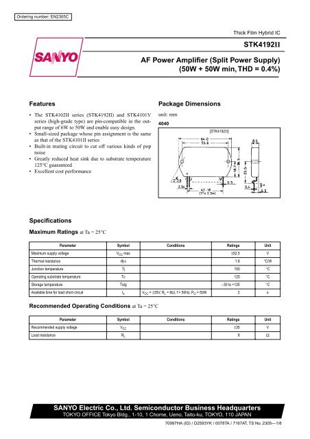
Ordering number: EN2305CThick Film Hybrid IC<strong>STK4192</strong>IIAF Power Amplifier (Split Power Supply)(50W + 50W min, THD = 0.4%)Features• The STK4102II series (<strong>STK4192</strong>II) and STK4101Vseries (high-grade type) are pin-compatible in the outputrange of 6W to 50W and enable easy design.• Small-sized package whose pin assignment is the sameas that of the STK4101II series• Built-in muting circuit to cut off various kinds of popnoise• Greatly reduced heat sink due to substrate temperature125°C guaranteed• Excellent cost performancePackage Dimensionsunit: mm4040[<strong>STK4192</strong>II]SpecificationsMaximum Ratings at Ta = 25°CParameter Symbol Conditions Ratings UnitMaximum supply voltage V CC max ±52.5 VThermal resistance θj-c 1.8 °C/WJunction temperature Tj 150 °COperating substrate temperature Tc 125 °CStorage temperature Tstg −30 to +125 °CAvailable time for load short-circuit t s V CC = ±35V, R L = 8Ω, f = 50Hz, P O = 50W 2 sRecommended Operating Conditions at Ta = 25°CParameter Symbol Conditions Ratings UnitRecommended supply voltage V CC ±35 VLoad resistance R L 8 ΩSANYO Electric Co., Ltd. Semiconductor Business HeadquartersTOKYO OFFICE Tokyo Bldg., 1-10, 1 Chome, Ueno, Taito-ku, TOKYO, 110 JAPAN70997HA (ID) / D2593YK / 0078TA / 7167AT, TS No. 2305—1/8
<strong>STK4192</strong>IIOperating Characteristics at Ta = 25°C, V CC = ±35V, R L = 8Ω, Rg = 600Ω, VG = 40dB,R L : non-inductive loadParameter Symbol Conditions min typ max UnitQuiescent current I CCO V CC = ±42V 20 40 100 mAOutput powerP O (1)THD = 0.4%,f = 20Hz to 20kHz50 WP O (2)V CC = ±31V, THD = 1.0%,R L = 4Ω, f = 1kHz55 WTotal harmonic distortion THD P O = 1.0W, f = 1kHz 0.3 %Frequency response f L , f H+0P O = 1.0W, dB–320 to 50k HzInput impedance r i P O = 1.0W, f = 1kHz 55 kΩOutput noise voltage V NO V CC = ±42V, Rg = 10kΩ 1.2 mVrmsNeutral voltage V N V CC = ±42V –70 0 +70 mVMuting voltage V M –2 –5 –10 VNotes.For power supply at the time of test, use a constant-voltage power supplyunless otherwise specified.For measurement of the available time for load short-circuit and outputnoise voltage, use the specified transformer power supply shown right.The output noise voltage is represented by the peak value on rms scale(VTVM) of average value indicating type. For AC power supply, use anAC stabilized power supply (50Hz) to eliminate the effect of flicker noisein AC primary line.Equivalent CircuitSpecified Transformer Power Supply(Equivalent to MG-200)No. 2305—2/8
<strong>STK4192</strong>IISample Application Circuit : 50W min 2-channel AF power amplifierSample Printed Circuit Pattern for Application Circuit (Cu-foiled side)No. 2305—3/8
<strong>STK4192</strong>IIOutput power, P O - WInput voltage, Vi - mVOutput power, P O - WTotal harmonic distortion, THD - %Output power, P O - WFrequency, f - HzVoltage gain, VG - dBQuiescent current, Icco - mANeutral voltage, V N - mVOutput power, P O - WTotal harmonic distortion, THD - %Frequency, f - HzOperating substrate temperature, Tc - °CNo. 2305—4/8
<strong>STK4192</strong>IIQuiescent current, Icco - mANeutral voltage, V N - mVSupply voltage, V CC - VSupply voltage, V CC - VOutput power, P O - WVoltage gain, VG - dBIC power dissipation, Pd - WIC power dissipation, Pd - WOutput power, P O - WOutput power, P O - WFrequency, f - HzNo. 2305—5/8
<strong>STK4192</strong>IISample Application Circuit (protection circuit and muting circuit)Thermal DesignThe IC power dissipation of the <strong>STK4192</strong>II at the IC-operated mode is 66W max. at load resistance 8Ω and 103W max.at load resistance 4Ω (simultaneous drive of 2 channels) for continuous sine wave as shown in Figure 1 and 2.IC Power dissipation, Pd - WIC Power dissipation, Pd - WOutput power, P O - WOutput power, P O - WFigure 1. <strong>STK4192</strong>II Pd – P O (R L = 8Ω) Figure 2. <strong>STK4192</strong>II Pd – P O (R L = 4Ω)No. 2305—7/8
<strong>STK4192</strong>IIIn an actual application where a music signal is used, it is impractical to estimate the power dissipation based on the continuoussignal as shown above, because too large a heat sink must be used. It is reasonable to estimate the power dissipationas 1/10 Po max. (EIAJ).That is, Pd = 43W at 8Ω, Pd = 55W at 4ΩThermal resistance θc-a of a heat sink for this IC power dissipation (Pd) is fixed under conditions 1 and 2 shown below.Condition 1: Tc = Pd × θc-a + Ta ≤ 125°C............................................... (1)where Ta : Specified ambient temperatureTc : Operating substrate temperatureCondition 2: Tj= Pd × (θc-a) + Pd/4 × (θj-c) + Ta ≤ 150°C..................... (2)where Tj : Junction temperature of power transistorAssuming that the power dissipation is shared equally among the four power transistors (2 channels × 2), thermal resistanceθj-c is 1.8°C/W andPd × (θc-a + 1.8/4) + Ta ≤ 150°C........................................ (3)Thermal resistance θc-a of a heat sink must satisfy inequalities(1) and (3).Figure 3 shows the relation between Pd and θc-a givenfrom (1) and (3) with Ta as a parameter.[Example] The thermal resistance of a heat sink isobtained when the ambient temperature specifiedfor a stereo amplifier is 50°C.Assuming V CC = ±35V, R L = 8Ω, V CC = ±31V, R L = 4Ω,R L = 8Ω : Pd1 = 43W at 1/10 Po max.R L = 4Ω : Pd2 = 55W at 1/10 Po max.The thermal resistance of a heat sink isobtained from Figure 3.R L = 8Ω : θc-a1 = 1.75°C/WR L = 4Ω : θc-a2 = 1.35°C/WTj when a heat sink is used is obtained from(3).R L = 8Ω : Tj = 144.6°CR L = 4Ω : Tj = 149°CThermal resistance of heat sink, θc-a - °C/WIC Power dissipation, Pd - WFigure 3. <strong>STK4192</strong>II θc-a – Pd■■■No products described or contained herein are intended for use in surgical implants, life-support systems, aerospace equipment, nuclearpower control systems, vehicles, disaster/crime-prevention equipment and the like, the failure of which may directly or indirectly cause injury,death or property loss.Anyone purchasing any products described or contained herein for an above-mentioned use shall:➀ Accept full responsibility and indemnify and defend SANYO ELECTRIC CO., LTD., its affiliates, subsidiaries and distributors and all theirofficers and employees, jointly and severally, against any and all claims and litigation and all damages, cost and expenses associatedwith such use:➁ Not impose any responsibility for any fault or negligence which may be cited in any such claim or litigation on SANYO ELECTRIC CO.,LTD., its affiliates, subsidiaries and distributors or any of their officers and employees, jointly or severally.Information (including circuit diagrams and circuit parameters) herein is for example only; it is not guaranteed for volume production. SANYObelieves information herein is accurate and reliable, but no guarantees are made or implied regarding its use or any infringements ofintellectual property rights or other rights of third parties.This catalog provides information as of July, 1997. Specifications and information herein are subject to change without notice.No. 2305—8/8
This <strong>datasheet</strong> has been download from:www.<strong>datasheet</strong>catalog.com<strong>Datasheet</strong>s for electronics components.