A 35-GS/s, 4-Bit Flash ADC With Active Data and ... - IEEE Xplore
A 35-GS/s, 4-Bit Flash ADC With Active Data and ... - IEEE Xplore
A 35-GS/s, 4-Bit Flash ADC With Active Data and ... - IEEE Xplore
- No tags were found...

Create successful ePaper yourself
Turn your PDF publications into a flip-book with our unique Google optimized e-Paper software.
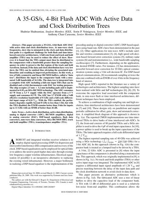
<strong>IEEE</strong> JOURNAL OF SOLID-STATE CIRCUITS, VOL. 44, NO. 6, JUNE 2009 1709A <strong>35</strong>-<strong>GS</strong>/s, 4-<strong>Bit</strong> <strong>Flash</strong> <strong>ADC</strong> <strong>With</strong> <strong>Active</strong> <strong>Data</strong><strong>and</strong> Clock Distribution TreesShahriar Shahramian, Student Member, <strong>IEEE</strong>, Sorin P. Voinigescu, Senior Member, <strong>IEEE</strong>, <strong>and</strong>Anthony Chan Carusone, Senior Member, <strong>IEEE</strong>Abstract—This paper presents a <strong>35</strong>-<strong>GS</strong>/s, 4-bit flash <strong>ADC</strong>-DACwith active data <strong>and</strong> clock distribution trees. At mm-wave clockfrequencies, skew due to mismatch in the clock <strong>and</strong> data distributionpaths is a significant challenge for both flash <strong>and</strong> time-interleavedconverter architectures. A full-rate front-end track <strong>and</strong> holdamplifier (THA) may be used to reduce the effect of skew. However,it is found that the THA output must then be distributed tothe comparators with a b<strong>and</strong>width greater than the sampling frequencyin order to preserve the flat regions of the track <strong>and</strong> holdwaveform. Instead, if the data <strong>and</strong> clock distribution have very lowskew, the THA can be omitted thus obviating the associated nonlinearities<strong>and</strong> resulting in improved performance. In this work, atree of fully symmetric <strong>and</strong> linear BiCMOS buffers, called a “datatree”, distributes the input to the comparator bank with a measured3-dB b<strong>and</strong>width of 16 GHz. The data tree is integrated intoa complete 4-bit <strong>ADC</strong> including a full-rate input THA that can bedisabled <strong>and</strong> a 4-bit thermometer-code DAC for testing purposes.The chip occupies 2.5 mm 3.2 mm including pads <strong>and</strong> is implementedin 0.18 m SiGe BiCMOS technology. The <strong>ADC</strong> consumes4.5 W from a 3.3 V supply while the DAC operates from a 5 Vsupply <strong>and</strong> consumes 0.5 W. The <strong>ADC</strong> has 3.7 ENOB with a 3-dBeffective resolution b<strong>and</strong>width of 8 GHz <strong>and</strong> a full-scale differentialinput range of 0.24 . <strong>With</strong> the THA enabled, the performancedegrades rapidly beyond 8 GHz to less than 1-bit, but withthe THA disabled, the ENOB remains better than 3-bits for inputsup to 11 GHz with an SFDR of better than 26 dB.Index Terms—<strong>Active</strong> clock distribution, active data distribution,analog to digital converter (<strong>ADC</strong>), BiCMOS amplifiers, digitalto analog converter (DAC), DSP-based equalizers, flash dataconverters, mm-wave data converters, SiGe BiCMOS HBT, track<strong>and</strong> hold amplifier (THA), transimpedance amplifier (TIA).I. INTRODUCTIONAROBUST <strong>and</strong> integrated wireline receiver solution is toemploy digital signal processing (DSP) for dispersion <strong>and</strong>intersymbol interference (ISI) compensation <strong>and</strong> recovery of theclock. DSP-based equalization can be employed for optical linksor to address the need to push higher data rates through existinglow frequency copper wireline infrastructures. Electrical equalization(if possible) is an inexpensive alternative to replacingthe existing wired infrastructure. However, a major bottleneckin realizing a DSP-based equalizer is the implementation of theManuscript received June 10, 2008; revised March 12, 2009. Current versionpublished May 28, 2009. This work was supported by Gennum <strong>and</strong> Jazz Semiconductor.The authors are with the Edward S. Rogers Sr. Department of Electrical <strong>and</strong>Computer Engineering, University of Toronto, Toronto, ON, Canada (e-mail:sshahram@eecg.utoronto.ca).Digital Object Identifier 10.1109/JSSC.2009.2020657preceding analog-to-digital converter (<strong>ADC</strong>). DSP-based equalizersusing baud-rate <strong>ADC</strong>s have been demonstrated in the past[1], [2]. Other applications for mm-wave <strong>ADC</strong>s include satellite<strong>and</strong> wireless communication [3], [4], high speed soft-decision-basedforward error correction systems [5], military radarsystems [6] <strong>and</strong> instrumentation (i.e., wide b<strong>and</strong>width samplingoscilloscopes) [7]. Furthermore, depending on the application,the desired ENOB varies. For instance, [3] has demonstrated apowerful forward error correction for 10 Gb/s optical communicationsystems using a 3-bit soft decision IC. For DSP-basedoptical communications, [8] recommends sampling at twice thedata rate combined with an ENOB of over 4 bits in the frequencyb<strong>and</strong> of interest.High speed <strong>ADC</strong>s reported in the literature use a variety oftechnologies <strong>and</strong> architectures. The highest sampling rates havebeen realized with SiGe <strong>and</strong> InP technologies [6], [8], [9]. Toovercome the capacitive load associated with the comparatorbank, in mm-wave flash or time interleaved architectures, differenttechniques have been employed.To achieve a combination of high sampling rate <strong>and</strong> high resolution,time-interleaved architectures have been demonstratedin [7] <strong>and</strong> [10]. These designs rely on parallelism <strong>and</strong> requireperiodic calibration for offset, gain, skew <strong>and</strong> mismatch correction.A simplified block diagram of this approach is shown inFig. 1(a). The reported CMOS implementations use time-interleavedTHAs to drive banks of time interleaved sub-<strong>ADC</strong>s. In[7], the front-end consists of 80 parallel THAs <strong>and</strong> a SiGe amplifieris used to drive the 4 pF of total input capacitance. In [10],a power splitter is used to break up the input capacitance of theTHAs. The latter approach requires a full scale differential inputof 1.2 .The highest reported sampling rate of 40 GHz was achievedusing a SiGe technology GHz for a3-bit <strong>ADC</strong> [6]. In this approach (shown in Fig. 1(b)) the comparatorbank is treated as a lumped load to be driven by a THA.A 5-bit, 22 <strong>GS</strong>/s <strong>ADC</strong> is presented in [8] where the inputcapacitance of the comparators is absorbed along a transmissionline. This approach, which was originally implemented in [9], isshown in Fig. 1(c). No track-<strong>and</strong>-hold amplifier (THA) or otheractive input stage was integrated. The implemented <strong>ADC</strong> in [8]requires a differential input signal amplitude of 1.28 <strong>and</strong>precise matching between the delay of the input data path <strong>and</strong>the clock distribution network to avoid clock-to-data skew.This paper presents an alternative architecture which isshown in Fig. 1(d). The fabricated <strong>ADC</strong> uses a tree of linearbuffers to drive the capacitive load of the comparator bank.A TIA with 12 dB of differential gain is used as a relativelylow-noise front-end amplifier. This combination allows the0018-9200/$25.00 © 2009 <strong>IEEE</strong>
1710 <strong>IEEE</strong> JOURNAL OF SOLID-STATE CIRCUITS, VOL. 44, NO. 6, JUNE 2009frequency input signals. Measurements of a fabricated breakoutcomprising a THA followed by an active data tree are alsopresented. The implementation <strong>and</strong> measurement results ofthe fabricated <strong>35</strong>-<strong>GS</strong>/s flash <strong>ADC</strong> is discussed in Section III.Concluding remarks are presented in Section IV.II. IMPACT OF THE ACTIVE DATA TREE ON <strong>ADC</strong> PERFORMANCEBy using a tree of linear buffers to drive the comparators of the<strong>ADC</strong>, the large capacitance associated with the comparator bankis divided amongst buffers with reduced fan-out. Since the inputcapacitance of the data tree is significantly smaller than that ofthe entire comparator bank, a high gain front-end amplifier (inthis design, a TIA) can then be used to drive the data tree withsufficient b<strong>and</strong>width (Fig. 1(d)). It is important to note however,that in contrast to purely passive data distribution, this activeimplementation consumes power.A simple approach is to design the data tree using identicalamplifiers with a fan-out of , in which case the required depthof the tree isfor an n-bit flash converter. In orderto minimize the number of cascaded stages, the highest fan-outwhich satisfies the overall required data tree b<strong>and</strong>width mustbe chosen. In practice, layout considerations <strong>and</strong> symmetry requirementsof the data tree must also be considered. To achievea data tree b<strong>and</strong>width of , each buffer with a fan-out ofmust have a 3 dB frequency of at least [11](1)In an -bit converter <strong>and</strong> under otherwise ideal conditions,a front-end amplifier <strong>and</strong> data tree b<strong>and</strong>width of canachieve an ENOB of better than (n-0.5)-bits up to the Nyquistfrequency. However, sources of sampling uncertainty canfurther degrade the performance of the <strong>ADC</strong>. The maximumachievable SNR in the presence of sampling jitter is [12](2)Fig. 1. <strong>Flash</strong> converter architectures: (a) A time interleaved architecture withsub-rate THAs <strong>and</strong> multiphase clock generator (e.g., [7], [10]). (b) Direct drivingthe comparator bank using a full rate THA (e.g., [6]). (c) Using a transmissionline to distribute the input <strong>and</strong> the clock signal (e.g., [8]). (d) Implementation ofactive distribution networks to route the input <strong>and</strong> clock signal to the comparatorbank, as in this work.<strong>ADC</strong> to process small input signals (0.24 differential), <strong>and</strong>drive the comparator bank through a symmetric data tree forminimized skew. A fully symmetric bipolar clock distributionnetwork is employed to minimize clock skew. This techniquerelies only on the matching between identical blocks in eachdistribution tree. A THA may be inserted between the front-endamplifier <strong>and</strong> the data tree, but it will be shown that unlesssufficient b<strong>and</strong>width is provided in the data tree such a track<strong>and</strong> hold amplifier can actually degrade the performance ofthe <strong>ADC</strong>. Section II discusses the impact of the data tree onthe <strong>ADC</strong> performance <strong>and</strong> the efficacy of the THA for highIn flash <strong>ADC</strong>s, three major sources of timing uncertainty areclock skew, data skew <strong>and</strong> r<strong>and</strong>om jitter of the clock signal,but clock <strong>and</strong> data skew dominate if the <strong>ADC</strong> is driven bya low phase noise clock [8]. To combat clock <strong>and</strong> data skewin mm-wave <strong>ADC</strong>s, a THA may be employed. A full rateTHA can be inserted after the front-end amplifier. For half theclock period the THA holds the input signal constant, ideallyreducing the rate of change of the input signal to zero. Duringthis time, the clocked comparators make decisions based on theheld value. For the second half of the clock period, the THAtracks the input signal. In the presence of an ideal THA, thesampling uncertainty due to clock <strong>and</strong> data skew is eliminated.The THA produces the desired “zero slope” regions in thetime domain by introducing high frequency content to the spectrumof the input signal. This high frequency content must bepreserved otherwise the hold mode behavior of the THA is lost.In practice, poles introduced at the output of the THA <strong>and</strong> comparatorpre-amplifiers attenuate this content, thus reducing theefficacy of the THA. Fig. 2 shows the block diagram of a 4-bitflash <strong>ADC</strong> used to model this phenomenon. In our behavioral
SHAHRAMIAN et al.: A <strong>35</strong>-<strong>GS</strong>/s, 4-<strong>Bit</strong> FLASH <strong>ADC</strong> WITH ACTIVE DATA AND CLOCK DISTRIBUTION TREES 1711Fig. 2. This model is used to simulate the efficacy of a THA in the presence of data tree b<strong>and</strong>width limitations. <strong>With</strong>out sufficient data tree b<strong>and</strong>width, the THAis unable to combat the effects of the clock <strong>and</strong> data skew ( <strong>and</strong> , respectively).Fig. 3. Impact of the data tree b<strong>and</strong>width on the THA waveform: (a) ! =2! , (b) ! =0:8! , (c) ! =0:5! . The input signal frequency is! =0:14! . The hold mode behavior of the THA is mostly lost if the data tree b<strong>and</strong>width is limited.simulations, an ideal THA is followed by anfilterth order low-pass<strong>and</strong> with a 3 dB b<strong>and</strong>width of . The low-pass filter representsthe frequency response of the data tree. For a constant 3 dBb<strong>and</strong>width, simulation results are similar for. Theresults shown here are for . Clock <strong>and</strong> data skew are modeledby delaying the input <strong>and</strong> clock of each comparator by independentGaussian distributed r<strong>and</strong>om variables ( <strong>and</strong>in Fig. 2) with zero mean <strong>and</strong> st<strong>and</strong>ard deviations ofwhere is the clock period of the <strong>ADC</strong>. Behavioralsimulations of one hundred 4-bit <strong>ADC</strong>s with a data tree b<strong>and</strong>widthof <strong>and</strong> no THA show that with increasing inputfrequency, the average ENOB decreases due to skew. For instance,while 95% of all simulated <strong>ADC</strong>s achieve an ENOB ofbetter than 3.5 bits for an input frequency of , only 3%(3)of the simulated <strong>ADC</strong>s achieve the same ENOB for an input frequencyof .An ideal THA followed by a data tree with infinite b<strong>and</strong>widthcan fully eliminate the effect of the skew in more than 99.7% ofall simulated <strong>ADC</strong>s resulting in an ENOB of 4-bits for any inputfrequency. However, an ideal THA followed by a finite-b<strong>and</strong>widthdata tree can be expected to have performance somewherebetween these two extremes. The goal is to investigate the datatree b<strong>and</strong>width requirements such that a THA can successfullycombat skew.Fig. 3 shows the input to the comparator bank for a sinusoidalinput signal with whereis the clock frequency of <strong>ADC</strong> in rad/s. <strong>With</strong> a very highb<strong>and</strong>width data tree, the slope during the hold time is zero, providingimmunity against skew. However, as the b<strong>and</strong>width is reduced,the input to the comparator bank looks increasingly likea sinusoid at the <strong>ADC</strong> input. Hence, the THA provides littleimprovement in performance unless the b<strong>and</strong>width of the followingstages is high enough.
1712 <strong>IEEE</strong> JOURNAL OF SOLID-STATE CIRCUITS, VOL. 44, NO. 6, JUNE 2009Fig. 4. Simulated ENOB of a 4-bit <strong>Flash</strong> <strong>ADC</strong> in the presence of clock <strong>and</strong> data skew with st<strong>and</strong>ard deviations of 0:05Ttree b<strong>and</strong>width is limited to 0:5! , a THA offers little improvement in performance.. It can be observed that if the dataThe simulated <strong>ADC</strong> ENOB profile is shown in Fig. 4. It showsthe minimum ENOB achieved by the best 95% of all simulated<strong>ADC</strong>s. <strong>With</strong> a data tree b<strong>and</strong>width of , no THA, <strong>and</strong> inthe presence of skew, an ENOB better than 3-bits can only beexpected for input frequencies up to . <strong>With</strong> the THAenabled <strong>and</strong> the data tree b<strong>and</strong>width extended to beyond ,nearly all simulated <strong>ADC</strong>s achieved 4-bits of ENOB. However,it can be observed that if the b<strong>and</strong>width of the data tree is closeto the Nyquist frequency,, implementing a THAgives little improvement in performance. Therefore, if a THAis to be employed effectively, the b<strong>and</strong>width of the data treemust exceed the clock frequency; typically a very difficult designspecification for mm-wave conversion rates.A. THA <strong>and</strong> <strong>Data</strong> Tree BreakoutTo investigate the impact of the data tree on the <strong>ADC</strong> performance,a breakout of the TIA, THA <strong>and</strong> data tree has been fabricated.This breakout allows for the characterization of the TIA,THA, <strong>and</strong> the BiCMOS data tree. The front-end amplifier is alow noise broadb<strong>and</strong> TIA, followed by a buffering stage whichdrives the THA. The buffering stage provides biasing currentto the THA <strong>and</strong> improves the single-ended to differential conversionwhen the TIA is driven single-ended [14]. Unlike [6],[7], [10], the implemented THA needs to only drive a smalloutput capacitance. A data tree of BiCMOS cascode buffersis employed. The tree is intended for use in a 4-bit flash converter.Each stage has a fan-out of two <strong>and</strong>, to save area in thisbreakout, only one branch of the tree is implemented with theother branches terminated on chip. A BiCMOS 50 driver allowsthe analog output of the tree to be taken off-chip.1) Transimpedance Amplifier (TIA): A transimpedanceamplifier can be designed to provide simultaneous noise <strong>and</strong>impedance matching without the need for 50 matching resistors[13]. Fig. 5 shows the schematic of the TIA included inthis <strong>ADC</strong>. The TIA is employed as the front-end amplifier <strong>and</strong>Fig. 5. Schematic of the implemented fully bipolar TIA. The TIA has 12 dBof simulated differential gain <strong>and</strong> drives the THA.is driven as a voltage amplifier. In order to achieve the desired12 dB of differential gain, the TIA is implemented using SiGeHBTs only. In this design, we have added 12 degenerationresistors to improve the linearity of the TIA without significantlydegrading the noise figure. Diode connected transistors<strong>and</strong> prevent the breakdown of <strong>and</strong> . A switchedemitter-follower THA is also implemented following the design
SHAHRAMIAN et al.: A <strong>35</strong>-<strong>GS</strong>/s, 4-<strong>Bit</strong> FLASH <strong>ADC</strong> WITH ACTIVE DATA AND CLOCK DISTRIBUTION TREES 1713Fig. 6. Schematic of the MOS-HBT cascode differential pair used in the datatree. CMOS input transistors offer high linearity while the bipolar cascode transistorsoffer low output capacitance.methodology described in [14]. The TIA has a simulated b<strong>and</strong>widthof better than 20 GHz. This simulation is also supportedby the measurement results presented in [14].2) BiCMOS <strong>Data</strong> Tree: Each block in the BiCMOS datatree consists of a MOS-HBT cascode amplifier shown in Fig. 6.The BiCMOS cascode amplifiers have a tail current of 8 mAwith the MOSFETs biased near the peak current densitymA m . Although smaller nMOS transistors aremore susceptible to mismatches, biasing at was necessaryto achieve a combination of high b<strong>and</strong>width <strong>and</strong> high linearity.In this design, the layout of each data tree block is optimizedby using dummy resistors, transistors <strong>and</strong> interdigitating <strong>and</strong>merging the nMOS transistors with common sources a singlewell to minimize mismatches. The 0.18 m nMOS pair offersa simulated differential input compression point of 1.5 atlow frequencies. The HBT common-base transistors create lowimpedance cascode nodes with high output slew rate <strong>and</strong> b<strong>and</strong>width.The data tree is implemented completely symmetricallyto minimize systematic sources of skew, comparator dependentsignal attenuation <strong>and</strong> offsets. Series-shunt inductive peaking isalso used throughout the data tree. Series peaking is providedby the interconnect between the data tree blocks. The simulatedb<strong>and</strong>width of a single block with a fan-out of two is 45 GHz <strong>and</strong>the simulated gain of the entire data tree is 0 dB.B. THA <strong>and</strong> <strong>Data</strong> Tree Measurement ResultsAll measurements on the breakout are done single-ended <strong>and</strong>using wafer probing. The measured <strong>and</strong> post-extraction simulatedsmall-signal characteristics of the TIA, THA <strong>and</strong> the datatree are shown in Fig. 7. The BiCMOS output driver used todrive off-chip 50 loads has a simulated loss of 6 dB. Thecombination of the TIA, THA <strong>and</strong> the data tree has a 3 dBb<strong>and</strong>width of 16 GHz. The TIA input return loss is better than10 dB up to 20 GHz. Although a similar THA in the same technologydemonstrated a b<strong>and</strong>width exceeding 40 GHz [14], theb<strong>and</strong>width of this design is limited by the many buffer stagesrequired to drive the capacitive load of the comparator bank.While each buffer stage has a b<strong>and</strong>width of 45 GHz on its own,cascading four of them along with the THA <strong>and</strong> TIA greatlyreduces the overall b<strong>and</strong>width down to 16 GHz. Fig. 8 showsthe measured time domain outputs of the breakout for input frequencyGHz <strong>and</strong> clock frequency GHzwithout [Fig. 8(a)] <strong>and</strong> with [Fig. 8(b)] the THA enabled. It canbe observed that the hold mode behavior of the THA has nearlydisappeared in Fig. 8(b) due to the insufficient b<strong>and</strong>width of thedata tree.A significant disadvantage of enabling the switched emitterfollower(SEF) THA is that it introduces nonlinearities whichcan actually degrade the SNDR of the <strong>ADC</strong>. Two major sourcesof this are the nonlinear modulation of the base-emitter junctionvoltage of the SEF during the charging <strong>and</strong> dischargingof the hold capacitance [14], <strong>and</strong> the mixing of the harmonicsof the input signal with the clock signal which folds the harmonicsback into the Nyquist b<strong>and</strong>width of the converter. Fig. 9shows the measured output spectrum of a fabricated breakout,with <strong>and</strong> without the THA activated. To disable the THA, it isswitched to track-mode only. In the case where the THA is disabled[Fig. 9(a)], the second <strong>and</strong> third harmonics at the outputare mostly due to the nonlinearities of the TIA. However, oncethe THA is activated [Fig. 9(b)], mixed products of the inputsignal harmonics, as well as the clock feed-through signal, arepresent at the output. The third order harmonic also increasesin magnitude. Depending on the resolution of the <strong>ADC</strong> <strong>and</strong> theseverity of the clock jitter <strong>and</strong> skew, the benefit of a THA canoutweigh the nonlinearities introduced by it. However, in thecase where the data distribution b<strong>and</strong>width is insufficient forproper operation of the THA, it is better to omit the implementationof the THA altogether. In this work, since the data treeb<strong>and</strong>width is insufficient for proper operation of the THA at thetargeted clock frequencies, minimizing clock <strong>and</strong> data skew isof great importance. This criterion was strictly observed by designingsymmetric <strong>and</strong> well-matched clock <strong>and</strong> data distributiontrees.III. THE 4-bit FLASH <strong>ADC</strong>-DAC CHAINThe fabricated <strong>ADC</strong> uses the same TIA <strong>and</strong> BiCMOS datatree as the breakout <strong>and</strong> merges the buffer <strong>and</strong> THA. The blockdiagram of the implemented <strong>ADC</strong>-DAC chain is shown inFig. 10. The data tree of BiCMOS cascode buffers distributesthe THA output to the entire comparator bank. Each of the 15comparators, required for 4-bit operation, consists of an offsetamplifier, a high gain preamplifier, a flip-flop <strong>and</strong> a differentialpair. A 16th dummy comparator is also employed to maintainthe symmetry of the data tree <strong>and</strong> provide a single thermometercode output off-chip for testing. The comparator bank producesa 15-level thermometer code. For testing, a 15-level thermometercode DAC has been implemented on chip. No decoderlogic or bubble correction circuitry has been implemented. Theclock tree comprises 17 series-shunt inductively peaked bipolar
1714 <strong>IEEE</strong> JOURNAL OF SOLID-STATE CIRCUITS, VOL. 44, NO. 6, JUNE 2009Fig. 7. Small-signal characteristics of the fabricated breakout. Measured single-ended s-parameters <strong>and</strong> simulated single-ended gain of the TIA, THA, data tree<strong>and</strong> overall s-parameters of the breakout after extraction are shown. The combination of the TIA, THA <strong>and</strong> the data tree has a measured small-signal 3 dB b<strong>and</strong>widthof 16 GHz.Fig. 8. Measured output of the fabricated breakout: (a) THA OFF; (b) THAON. Due to the limited data tree b<strong>and</strong>width, the hold mode behavior of the THAamplifier is nearly eliminated.differential pairs with a fan-out of two per stage; the final stagesdrive four latches each. A separate clock path drives the THA.A two-stage tuneable delay cell has been implemented on chipto align the THA clock with the comparator clock. The activedelay cells consist of phase interpolating blocks between fastFig. 9. Measured spectra of the breakout output showing the nonlinearity impactof the THA: (a) THA disabled; (b) THA enabled showing intermodulationproducts of the input <strong>and</strong> clock signals in the output spectrum.<strong>and</strong> slow paths [15]. The THA can be disabled by forcing itinto track mode only via external controls.A. <strong>ADC</strong>-DAC Circuit Descriptions1) Merged BiCMOS Cascode <strong>and</strong> THA: In the design of the<strong>ADC</strong>, a MOS-HBT BiCMOS cascode buffer is merged with theswitched emitter-follower THA as shown in the schematics on
SHAHRAMIAN et al.: A <strong>35</strong>-<strong>GS</strong>/s, 4-<strong>Bit</strong> FLASH <strong>ADC</strong> WITH ACTIVE DATA AND CLOCK DISTRIBUTION TREES 1715Fig. 10.Block diagram of the implemented <strong>35</strong>-<strong>GS</strong>/s, 4-bit, <strong>Flash</strong> <strong>ADC</strong>-DAC. The <strong>ADC</strong> uses data <strong>and</strong> clock distribution to drive the comparator bank.Fig. 11. Schematic of the merged MOS-HBT BiCMOS cascode <strong>and</strong> THA. The total capacitance at node (a) is reduced by connecting the collector of transistorQ to the low impedance cascode node (b) instead.Fig. 11. The tail current of the THA is 6 mA per side. Comparedwith [14], the total capacitance at node (A) is reduced byconnecting the collector of transistor to the low impedancecascode node (B) instead. This approach eliminates the need forlevel shifting diodes, <strong>and</strong> further isolates the hold capacitor, ,from the clock signal.2) Comparator Design: Offset currents were used in thisdesign to establish the quantization levels without a resistor
1716 <strong>IEEE</strong> JOURNAL OF SOLID-STATE CIRCUITS, VOL. 44, NO. 6, JUNE 2009Fig. 12. Schematic of MOS-HBT BiCMOS cascode offset amplifier. The offset currents are drawn from the low impedance cascode nodes to mitigate their impacton b<strong>and</strong>width.ladder [6]. Each of the comparators is preceded by a differentialBiCMOS cascode offset amplifier illustrated in Fig. 12.The unit quantization current in this design is 120 A, whichin combination with the 170 load resistors, produces a differentialquantization level of 40.8 mV at the inputs of the comparators.Furthermore, since the simulated gain of the data treeis 0 dB, one LSB referred back to the input of the data treeis also 40.8 mV. The offset currents are drawn from the lowimpedance cascode nodes, (A) <strong>and</strong> (B), to mitigate their impacton b<strong>and</strong>width. In order to maintain equal delay, the totalcapacitance at nodes (A) <strong>and</strong> (B) is kept constant for all comparators.This is accomplished by adding dummy “off” currentsources where needed. Offset mismatches introduced by thedata tree also present themselves at the output of this block.These types of mismatches may be corrected by calibration ofthe offset currents. Similarly, data tree gain variations may alsobe corrected through this type of calibration. However, in thisdesign, due to the large quantization levels <strong>and</strong> the low datatree gain, no calibration technique has been deemed necessary.Fully bipolar cascode pre-amplifiers with 15 dB of differentialgain <strong>and</strong> 25 GHz b<strong>and</strong>width follow the BiCMOS offset amplifiers.The comparator’s metastability window, which refersto the smallest input voltage required to switch a comparator’sstate, is reduced by the addition of these pre-amplifiers. Thepreamplifiers also isolate the offset stages from flip-flop kickback.Each flip-flop has two latches with 4 mA tail current <strong>and</strong>emitter-followers both on the clock <strong>and</strong> data paths. Invertingstages with 4 mA tail current follow every flip-flop to eliminatethe latch induced clock feedthrough <strong>and</strong> drive the DAC. Thecombination of the pre-amplifier <strong>and</strong> flip-flop has a simulatedmetastability window of better than 20 mV at <strong>35</strong> Gbps.3) Thermometer Code DAC: The comparator bank producesa 15-level thermometer code. In implementations where thermometer-to-binaryconversion is required, bubble error removalcan be applied in the form of three-input NAND gates at thecost of increased power consumption [16]. Another method toremove bubble errors that does not increase the power consumptionis by adding extra “voting” transistors to the latches as proposedby [17]. However, in this approach the added capacitiveloading in the latches may reduce the maximum conversion frequency.For testing purposes, a 15-level thermometer code DAC hasbeen implemented on this chip. Its schematic is reproduced inFig. 13. It consists of a differential, double bipolar cascode. Eachthermometer code bit drives one CML inverter with a tail of currentof 4 mA. The output currents of these CML inverters aresummed in the first cascode nodes in groups of four. The remainingfour output currents are summed in the second cascodenodes in pairs. Finally the remaining two output currents aresummed at the on-chip 50 resistors. Simulations have shownthat, in this technology <strong>and</strong> with this DAC topology, bufferssmaller than 4 mA do not have sufficient b<strong>and</strong>width to operate at<strong>35</strong> Gbps. Each thermometer code produces a differential swingof 200 mV for a total differential output swing of 3 V . Theemitter-followers driving the inverting stages of the DAC operatefrom 3.3 V while the double cascodes require a 5 V powersupply (Fig. 13).4) Clock Distribution Network: The challenging task of distributingthe <strong>35</strong> GHz clock to 32 latches (16 master–slave comparators)is accomplished by a fully bipolar clock distributiontree. The tree consists of series-shunt inductively peaked stageswith a fan-out of two per stage; the final stages drive four latches
SHAHRAMIAN et al.: A <strong>35</strong>-<strong>GS</strong>/s, 4-<strong>Bit</strong> FLASH <strong>ADC</strong> WITH ACTIVE DATA AND CLOCK DISTRIBUTION TREES 1717Fig. 13. Schematic of the implemented 15-level thermometer code DAC. Thermometer code inputs (D0–D15) are summed together at different nodes of thedouble cascode DAC.Fig. 14. Chip micrograph of the <strong>ADC</strong>-DAC, die area is 2:5 2 3:2 mm .Fig. 15.Measured <strong>ADC</strong> INL <strong>and</strong> DNL with a <strong>35</strong>-GHz clock frequency.each. Each stage has an 8 mA tail current with 500 mV of differentialoutput swing. A separate clock path drives the THA. Atwo-stage tuneable delay cell is also implemented on chip [15].It is used to align the clock <strong>and</strong> data signals <strong>and</strong> consists of phaseinterpolating blocks between fast <strong>and</strong> slow paths.B. <strong>ADC</strong>-DAC Measurement ResultsThe <strong>ADC</strong>-DAC chain has been implemented in Jazz Semiconductor’sSBC18HX, 0.18 m SiGe BiCMOS HBT technology.The process offers an of 160 GHz/50 GHz for bipolar<strong>and</strong> nMOS devices respectively. The <strong>ADC</strong> operates from a 3.3 Vsupply while the DAC requires a 5 V supply. The chip occupies
1718 <strong>IEEE</strong> JOURNAL OF SOLID-STATE CIRCUITS, VOL. 44, NO. 6, JUNE 2009TABLE IPERFORMANCE SUMMARY AND COMPARISON TABLEMeasured at 2 <strong>GS</strong>/s.Measured at 20 <strong>GS</strong>/s <strong>and</strong> 10 GHz input. Includes the on-chip decoder power.Fig. 16. Measured ENOB <strong>and</strong> SFDR versus input frequency for a <strong>35</strong>-GHzclock frequency. The THA degrades the performance of the <strong>ADC</strong> for input frequenciesabove 8 GHz.an area of 2.5 mm 3.2 mm <strong>and</strong> the <strong>ADC</strong>-DAC chain consumesa total of 5 W (4.5 W for the <strong>ADC</strong>). The data <strong>and</strong> clocktree require 0.65 W <strong>and</strong> 1 W respectively. The comparator bankconsumes 2.4 W while the TIA <strong>and</strong> THA amplifier use a totalof 0.23 W. The adjustable delay cells <strong>and</strong> biasing circuitry needa total of 0.22 W. Fig. 14 shows the chip micrograph.The INL <strong>and</strong> DNL were measured differentially by applying afull scale DC sweep at the input <strong>and</strong> capturing the DAC outputswhile clocking the <strong>ADC</strong> at <strong>35</strong> GHz. Fig. 15 shows that the INL<strong>and</strong> DNL of the <strong>ADC</strong> are below 0.5 LSB for all analog inputlevels. The measured INL <strong>and</strong> DNL of the DAC are better than0.1 LSB for all digital codes.All dynamic measurements are performed singled-ended bywafer probing only one of the differential pair outputs. The <strong>ADC</strong>Fig. 17. Output spectrum of a 7.98 GHz input signal sampled at <strong>35</strong> GHz aftercorrections. The THA is disabled.was tested with the same input signal power for all input frequencies.After accounting for the sin(x)/x DAC roll-off <strong>and</strong>high frequency losses in the wafer probes <strong>and</strong> cables, the SFDR<strong>and</strong> ENOB of the <strong>ADC</strong> are plotted in Fig. 16 for both THA operationmodes. At low frequencies the ENOB is 3.7 bits (24 dBSNDR). Fig. 17 shows a sample output spectrum of a 7.98 GHzinput signal with the THA disabled. The effective resolutionb<strong>and</strong>width is about 8 GHz irrespective whether the THA is enabledor not. However, beyond 8 GHz the SFDR <strong>and</strong> ENOBdegrade more rapidly with the THA activated. This is the resultof the input signal harmonics mixing with the clock signal <strong>and</strong>showing up at low frequencies, within the b<strong>and</strong>width of the datatree. The third-order harmonics of the input signal is also degradeddue to the SEF THA nonlinearities. Therefore, the THAactually degrades the performance of this <strong>ADC</strong>. In this design,
SHAHRAMIAN et al.: A <strong>35</strong>-<strong>GS</strong>/s, 4-<strong>Bit</strong> FLASH <strong>ADC</strong> WITH ACTIVE DATA AND CLOCK DISTRIBUTION TREES 1719with 4 bits of precision, careful layout is sufficient to preventskew from becoming a performance limitation. Table I presentsa performance summary <strong>and</strong> comparison table.IV. CONCLUSIONA 4-bit, <strong>35</strong>-<strong>GS</strong>/s flash <strong>ADC</strong>-DAC chain was demonstratedin this paper. The <strong>ADC</strong> uses active clock <strong>and</strong> data trees to distributethe input <strong>and</strong> the clock to the comparators. Because bothclock <strong>and</strong> data are symmetrically distributed, this implementationminimizes timing skew achieving 3.7 ENOB with 8 GHz effectiveresolution b<strong>and</strong>width <strong>and</strong> 3 ENOB up to 11 GHz withoutthe full-rate THA.ACKNOWLEDGMENTThe authors would like to acknowledge Gennum for financialsupport, Jazz Semiconductor for fabrication, <strong>and</strong> CMC for CADtools.REFERENCES[1] M. Harwood, N. Warke, R. Simpson, T. Leslie, A. Amerasekera, S.Batty, D. Colman, E. Carr, V. Gopinathan, S. Hubbins, P. Hunt, A.Joy, P. Kh<strong>and</strong>elwal, B. Killips, T. Krause, S. Lytollis, A. Pickering, M.Saxton, D. Sebastio, G. Swanson, A. Szczepanek, T. Ward, J. Williams,R. Williams, <strong>and</strong> T. Willwerth, “A 12.5 Gb/s SerDes in 65 nm CMOSusing a baud-rate <strong>ADC</strong> with digital receiver equalization <strong>and</strong> clock recovery,”in <strong>IEEE</strong> Int. Solid-State Circuits Conf. (ISSCC) Dig. Tech. Papers,2007, pp. 436–437.[2] H. Bae, J. B. Ashbrook, J. Park, N. R. Shanbhag, A. C. Singer, <strong>and</strong> S.Chopra, “An MLSE receiver for electronic dispersion compensation ofOC-192 fiber links,” <strong>IEEE</strong> J. Solid-State Circuits, vol. 41, no. 11, pp.2541–2554, Nov. 2006.[3] J. C. Jensen <strong>and</strong> L. E. Larson, “A broadb<strong>and</strong> 10 GHz track-<strong>and</strong>-hold inSi/SiGe HBT technology,” <strong>IEEE</strong> J. Solid-State Circuits, vol. 36, no. 3,pp. 325–330, Mar. 2001.[4] Y. Lu, W.-M. Kuo, X. Li, R. Krithivasan, J. D. Cressler, Y.Borokhovych, H. Gustat, B. Tillack, <strong>and</strong> B. Heinemann, “An8-bit 12 Gsample/sec SiGe track-<strong>and</strong>-hold amplifier,” in Proc.Bipolar/BiCMOS Circuits <strong>and</strong> Technology Meeting (BCTM), 2005,pp. 148–151.[5] H. Tagami, T. Kobayashi, Y. Miyata, K. Ouchi, K. Sawada, K. Kubo,K. Kuno, H. Yoshida, K. Shimizu, T. Mizuochi, <strong>and</strong> K. Motoshima, “A3-bit soft-decision IC for powerful forward error correction in 10-Gb/soptical communication systems,” <strong>IEEE</strong> J. Solid-State Circuits, vol. 40,no. 8, pp. 1695–1705, Aug. 2005.[6] W. Cheng, W. Ali, M.-J. Choi, K. Liu, T. Tat, D. Devendorf, L. Linder,<strong>and</strong> R. Stevens, “A 3 b 40 <strong>GS</strong>/s <strong>ADC</strong>-DAC in 0.12 m SiGe,” in <strong>IEEE</strong>Int. Solid-State Circuits Conf. (ISSCC) Dig. Tech. Papers, 2004, pp.262–263.[7] K. Poulton, R. Neff, B. Setterberg, B. Wuppermann, T. Kopley, R.Jewett, J. Pernillo, C. Tan, <strong>and</strong> A. Montijo, “A 20 <strong>GS</strong>/s 8 b <strong>ADC</strong> witha 1 MB memory in 0.18 m CMOS,” in <strong>IEEE</strong> Int. Solid-State CircuitsConf. (ISSCC) Dig. Tech. Papers, 2003, pp. 318–319.[8] P. Schvan, D. Pollex, S. Wang, C. Falt, <strong>and</strong> N. Ben-Hamida, “A 22<strong>GS</strong>/s 5 b <strong>ADC</strong> in 0.13 m SiGe BiCMOS,” in <strong>IEEE</strong> Int. Solid-StateCircuits Conf. (ISSCC) Dig. Tech. Papers, 2006, pp. 572–573.[9] H. Nosaka, M. Nakamura, M. Ida, K. Kurishima, T. Shibata, M. Tokumitsu,<strong>and</strong> M. Muraguchi, “A 24-Gsps 3-bit Nyquist <strong>ADC</strong> using InPHBTs for electronic dispersion compensation,” in 2004 <strong>IEEE</strong> MTT-SInt. Microwave Symp. Dig., 2004, pp. 101–104.[10] P. Schvan, J. Bach, C. Falt, P. Flemke, R. Gibbins, Y. Greshishchev,N. Ben-Hamida, D. Pollex, J. Sitch, S.-C. Wang, <strong>and</strong> J. Wolczanski, “A24 <strong>GS</strong>/s 6 b <strong>ADC</strong> in 90 nm CMOS,” in <strong>IEEE</strong> Int. Solid-State CircuitsConf. (ISSCC) Dig. Tech. Papers, 2008, pp. 544–545.[11] E. Sackinger, Broadb<strong>and</strong> Circuits for Optical Fiber Communications.New York: Wiley, 2005.[12] M. Shinagawa, Y. Akazawa, <strong>and</strong> T. Wakimoto, “Jitter analysis of highspeedsampling systems,” <strong>IEEE</strong> J. Solid-State Circuits, vol. 25, no. 2,pp. 220–224, Feb. 1990.[13] H. Tran, F. Pera, D. S. McPherson, D. Viorel, <strong>and</strong> S. P. Voinigescu,“6-k 43-Gb/s differential transimpedance-limiting amplifier withauto-zero feedback <strong>and</strong> high dynamic range,” <strong>IEEE</strong> J. Solid-StateCircuits, vol. 39, no. 10, pp. 1680–1689, Oct. 2004.[14] S. Shahramian, A. C. Carusone, <strong>and</strong> S. P. Voinigescu, “Design methodologyfor a 40-Gsamples/s track <strong>and</strong> hold amplifier in 0.18-m SiGeBiCMOS technology,” <strong>IEEE</strong> J. Solid-State Circuits, vol. 41, no. 10, pp.2233–2240, Oct. 2006.[15] T. O. Dickson, E. Laskin, I. Khalid, R. Beerkens, J. Xie, B. Karajica,<strong>and</strong> S. P. Voinigescu, “An 80-Gb/s 2 -1 pseudor<strong>and</strong>om binary sequencegenerator in SiGe BiCMOS technology,” <strong>IEEE</strong> J. Solid-StateCircuits, vol. 40, no. 12, pp. 27<strong>35</strong>–2745, Dec. 2005.[16] M. Steyaert, R. Roovers, <strong>and</strong> J. Craninckx, “A 100 MHz 8 bit CMOSinterpolating A/D converter,” in Proc. <strong>IEEE</strong> Custom Integrated CircuitsConf. (CICC), May 1993, pp. 28.1.1–28.1.4.[17] J. van Valburg <strong>and</strong> R. J. van de Plassche, “An 8-b 650-MHz folding<strong>ADC</strong>,” <strong>IEEE</strong> J. Solid-State Circuits, vol. 27, no. 12, pp. 1662–1666,Dec. 1992.Shahriar Shahramian (S’06) received the B.A.Sc.(Hons) degree in computer engineering from the Universityof Toronto, Toronto, ON, Canada, in 2003.He enrolled in the Masters program in electrical engineeringat the University of Toronto in 2003 <strong>and</strong>transferred to the Ph.D. program in 2004. He is currentlyworking toward the Ph.D. degree in the Departmentof Electrical <strong>and</strong> Computer Engineering, Universityof Toronto.His research interests include the design of highspeed<strong>and</strong> mm-wave integrated circuits with focus onhigh-speed A/D converters <strong>and</strong> DSP-based equalizers. He also completed an internshipprogram at Alcatel-Lucent in 2008 where he worked on E-B<strong>and</strong> wirelesstransceivers.Mr. Shahramian received the Aloha Award in recognition of his B.A.Sc.thesis. He was also the recipient of the Ontario Graduate Scholarship in 2003<strong>and</strong> University of Toronto Fellowship from 2004 to 2006. He won the BestPaper Award at the Compound Semiconductor IC Symposium in 2005. He hasalso received six teaching awards between the years 2005–2008 at Universityof Toronto.Sorin P. Voinigescu (SM’02) received the M.Sc. degreein electronics from the Polytechnic Institute ofBucharest, Romania, in 1984, <strong>and</strong> the Ph.D. degreein electrical <strong>and</strong> computer engineering from the Universityof Toronto, Toronto, ON, Canada, in 1994.From 1984 to 1991, he worked in R&D <strong>and</strong>academia in Bucharest, where he designed <strong>and</strong>lectured on microwave semiconductor devices <strong>and</strong>integrated circuits. Between 1994 <strong>and</strong> 2002, hewas with Nortel Networks <strong>and</strong> Quake Technologiesin Ottawa, Canada, where he was responsible forprojects in high-frequency characterization <strong>and</strong> statistical scalable compactmodel development for Si, SiGe, <strong>and</strong> III-V devices. He later conducted researchon wireless <strong>and</strong> optical fiber building blocks <strong>and</strong> transceivers in these technologies.In 2002, he joined the University of Toronto, where he is a full Professor.He has authored or coauthored over 100 refereed <strong>and</strong> invited technical papersspanning the simulation, modeling, design, <strong>and</strong> fabrication of high frequencysemiconductor devices <strong>and</strong> circuits. His research <strong>and</strong> teaching interests focuson nanoscale semiconductor devices <strong>and</strong> their application in integrated circuitsat frequencies beyond 200 GHz.Dr. Voinigescu received the Nortel President Award for Innovation in 1996<strong>and</strong> is a member of the TPCs of the <strong>IEEE</strong> CSICS <strong>and</strong> BCTM. He is a co-recipientof the Best Paper Award at the 2001 <strong>IEEE</strong> CICC <strong>and</strong> at the 2005 <strong>IEEE</strong> CSICS,<strong>and</strong> of the Beatrice Winner Award at the 2008 <strong>IEEE</strong> ISSCC. His students havewon Best Student Paper Awards at the 2004 <strong>IEEE</strong> VLSI Circuits Symposium,the 2006 SiRF Meeting, 2006 RFIC Symposium, <strong>and</strong> 2006 BCTM.
1720 <strong>IEEE</strong> JOURNAL OF SOLID-STATE CIRCUITS, VOL. 44, NO. 6, JUNE 2009Anthony Chan Carusone (SM’08) received theB.A.Sc. <strong>and</strong> Ph.D. degrees from the University ofToronto, Toronto, ON, Canada, in 1997 <strong>and</strong> 2002,respectively, during which time he received theGovernor-General’s Silver Medal.Since 2001, he has been with the Department ofElectrical <strong>and</strong> Computer Engineering at the Universityof Toronto, where he is currently an AssociateProfessor. In 2008, he was a visiting researcher at theUniversity of Pavia, Italy, <strong>and</strong> later at the Circuits ResearchLab of Intel Corporation, Hillsboro, Oregon.Prof. Chan Carusone was a coauthor of the best paper at the 2005 CompoundSemiconductor Integrated Circuits Symposium <strong>and</strong> the best student papers atboth the 2007 <strong>and</strong> 2008 Custom Integrated Circuits Conferences. He is an appointedmember of the Administrative Committee of the <strong>IEEE</strong> Solid-State CircuitsSociety, a member <strong>and</strong> past chair of the Analog Signal Processing TechnicalCommittee for the <strong>IEEE</strong> Circuits <strong>and</strong> Systems Society, <strong>and</strong> a member<strong>and</strong> past chair of the Wireline Communications subcommittee of the CustomIntegrated Circuits Conference. He serves as a guest editor for both the <strong>IEEE</strong>JOURNAL OF SOLID-STATE CIRCUITS <strong>and</strong> the <strong>IEEE</strong> TRANSACTIONS ON CIRCUITSAND SYSTEMS I: REGULAR PAPERS. He is currently Editor-in-Chief of the <strong>IEEE</strong>TRANSACTIONS ON CIRCUITS AND SYSTEMS II: EXPRESS BRIEFS.