A 30-GS/sec Track and Hold Amplifier in 0.13-µm CMOS Technology
A 30-GS/sec Track and Hold Amplifier in 0.13-µm CMOS Technology
A 30-GS/sec Track and Hold Amplifier in 0.13-µm CMOS Technology
- No tags were found...

Create successful ePaper yourself
Turn your PDF publications into a flip-book with our unique Google optimized e-Paper software.
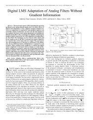
Fig. 3.Circuit diagram of the differential pair, T/H <strong>and</strong> output driver blocks. All MOSFETs have a drawn gate length of <strong>0.13</strong>µm.range. This is realized by choos<strong>in</strong>g a low noise broadb<strong>and</strong><strong>in</strong>put stage <strong>and</strong> bias<strong>in</strong>g the transistors <strong>in</strong> the data path at0.25 mA/µm for a good compromise between b<strong>and</strong>width, lownoise<strong>and</strong> high l<strong>in</strong>earity.A clock distribution network provides the differential clocksignal to the T/H block. It consists of the same TIA-CS frontendas the data path, followed by three CML <strong>in</strong>verters. Thesestages operate <strong>in</strong> digital mode <strong>and</strong> are biased at 0.15 mA/µmfor maximum switch<strong>in</strong>g speed. The circuit is powered froma 1.8-V supply <strong>and</strong> consumes 270 mW. The T/H block <strong>and</strong>the clock distribution network consume 12 mA <strong>and</strong> 70 mArespectively, while the rema<strong>in</strong><strong>in</strong>g 68 mA of current is drawnby the <strong>in</strong>put <strong>and</strong> output blocks.A. Transimpedance <strong>Amplifier</strong> (TIA)Instead of us<strong>in</strong>g 50Ω-term<strong>in</strong>ated differential pairs, this designemploys a low noise TIA <strong>in</strong>put stage (Fig. 2). A TIAprovides simultaneous noise <strong>and</strong> signal match<strong>in</strong>g without theneed for 50Ω match<strong>in</strong>g resistors. Noise match<strong>in</strong>g is achievedby siz<strong>in</strong>g the <strong>in</strong>put transistors (Q 1−2 ) to produce an optimumsource impedance of 50Ω [11]. The <strong>in</strong>put impedance is set bythe feedback resistor R F . Active PMOS loads (Q 3−4 ) are usedto <strong>in</strong>crease the open loop ga<strong>in</strong> <strong>and</strong> maximize the l<strong>in</strong>earity ofthe TIA. At DC, transistors Q 1 <strong>and</strong> Q 2 are diode connected<strong>and</strong> thus the output of the TIA biases the transistors Q 5−6[12]. The <strong>in</strong>put-referred noise power spectral density of thecascade of the TIA <strong>and</strong> the differential pair stages obta<strong>in</strong>edfrom simulation <strong>and</strong> <strong>in</strong>tegrated up to <strong>30</strong> GHz is 0.5 mV rms .B. <strong>Track</strong> <strong>and</strong> <strong>Hold</strong> StageFig. 3 shows the schematic diagram of the T/H amplifierwith a differential pair <strong>in</strong>put <strong>and</strong> output driver. In track mode,Clk P is high, Q SF acts as a source follower <strong>and</strong> the outputfollows the <strong>in</strong>put signal. In hold mode, Clk N is high <strong>and</strong> thetail current I T flows through the loads of the differential pair,R L .ThevalueofR L is chosen such that the voltage dropI T R L turns off transistor Q SF <strong>and</strong> provides good isolationbetween the <strong>in</strong>put <strong>and</strong> the output. The power supply voltagerequired by this design is dictated by I Diff R L + V <strong>GS</strong>−QSF +V <strong>GS</strong>−QDRV .Tak<strong>in</strong>g advantage of the triple well option <strong>in</strong> this process,the bulk <strong>and</strong> source of Q SF are shorted together to m<strong>in</strong>imizeV <strong>GS</strong>−QSF <strong>and</strong> allow for a 600-mV P −P signal sw<strong>in</strong>g at theoutput of the source follower. Even though a 1.8-V supply isrequired, the voltage drop across <strong>in</strong>dividual transistors does notexceed 1.2 V. The hold capacitance, C H = 250fF, <strong>in</strong>cludesthe parasitic capacitances at that node <strong>and</strong> a 50fF MIMcapacitor. The value of C fth is chosen to match C <strong>GS</strong>−QSF<strong>and</strong> to cancel hold mode signal feedthrough.C. Clock Distribution NetworkThe clock path converts a s<strong>in</strong>gle-ended <strong>30</strong>-GHz clock <strong>in</strong>putto a differential signal with 750mV P −P sw<strong>in</strong>g per side at thetwo switch<strong>in</strong>g pairs (Q T <strong>and</strong> Q H ) <strong>in</strong> the T/H block. The blocks<strong>in</strong> the clock path operate at <strong>30</strong> GHz, the highest operat<strong>in</strong>gfrequency of this circuit. It consists of a TIA stage (identicalto Fig. 2) followed by three CML <strong>in</strong>verters. The schematic ofthe f<strong>in</strong>al three CML <strong>in</strong>vert<strong>in</strong>g stages is shown <strong>in</strong> Fig. 4. Inorder to ensure that every stage is fully switched, the ga<strong>in</strong> ofthe <strong>in</strong>verters <strong>in</strong> the clock path is designed to exceed √ 2.III. FABRICATION AND TESTINGThe chip was fabricated <strong>in</strong> a <strong>0.13</strong>µm <strong>CMOS</strong> technology.The chip area is 1 mm 2 <strong>and</strong> the die photo is shown <strong>in</strong> Fig. 5.All measurements were conducted on-wafer with s<strong>in</strong>gle-ended<strong>in</strong>put <strong>and</strong> clock signal.The simulated <strong>and</strong> measured S-parameters are shown <strong>in</strong>Fig. 7. The <strong>in</strong>put <strong>and</strong> output return loss are better than -10 dB
Fig. 4.Circuit diagram of the f<strong>in</strong>al three CML <strong>in</strong>vert<strong>in</strong>g stages of the clock path. All MOSFETs have a drawn gate length of <strong>0.13</strong>µm.up to 35 GHz. S 21 has a b<strong>and</strong>width of 7 GHz when the circuitis operated <strong>in</strong> track mode. S<strong>in</strong>ce the front end of the data <strong>and</strong>clock paths are identical, the <strong>in</strong>put return loss of the data pathis also representative of the clock <strong>in</strong>put return loss which isless than -15 dB from 22 GHz to 32 GHz.Fig. 6 illustrates the two s<strong>in</strong>gle ended outputs for a -12 dBm,5-GHz <strong>in</strong>put signal sampled at <strong>30</strong> GHz. Signal droop rate wasmeasured at low clock frequencies to be less than 10 mV/ns.For a <strong>30</strong>-GHz sampl<strong>in</strong>g frequency, this translates to a droopof only 0.2 mV per held value.The <strong>in</strong>put <strong>and</strong> output compression po<strong>in</strong>ts of the circuit weremeasured from 1 GHz to 14 GHz <strong>in</strong> 1-GHz steps <strong>and</strong> areillustrated <strong>in</strong> Fig. 8. Fig. 9 shows the measured IIP3 <strong>and</strong>OIP3 as a function of frequency. The OIP3 plot <strong>in</strong>dicatesa circuit b<strong>and</strong>width of 7 GHz, <strong>in</strong> close agrement with theS 21 measurement. Simulations show that the hold node is theb<strong>and</strong>width-limit<strong>in</strong>g node of this circuit. The measured SFDR<strong>and</strong> THD are illustrated <strong>in</strong> Fig. 10. SFDR is calculated fromthe measured spectra <strong>and</strong> simulated noise floor <strong>in</strong>tegrated overa <strong>30</strong>-GHz b<strong>and</strong>width, (evaluated to be -53 dBm). The THAhas an SFDR of 40 dB at 1 GHz with 7 GHz of b<strong>and</strong>width.IV. CONCLUSIONSA <strong>30</strong>-<strong>GS</strong>/<strong>sec</strong> <strong>CMOS</strong> THA was designed <strong>and</strong> fabricated <strong>in</strong>a <strong>0.13</strong>-µm <strong>CMOS</strong> process. Follow<strong>in</strong>g a systematic designprocedure, <strong>and</strong> comb<strong>in</strong><strong>in</strong>g a low noise front-end with signalfeedthrough cancelation <strong>and</strong> power supply voltage reductiontechniques, has yielded the highest sampl<strong>in</strong>g frequency THA<strong>in</strong> <strong>CMOS</strong>. With a THD of better than -29 dB <strong>and</strong> 7 GHzof b<strong>and</strong>width, this THA is a potential contender for the frontend of a <strong>30</strong> <strong>GS</strong>/<strong>sec</strong> flash ADC. Such an ADC can be used <strong>in</strong>over-sampl<strong>in</strong>g DSP based receivers for 10 Gbps applications.Fig. 5.Die photo of the fabricated THAFig. 6.S<strong>in</strong>gle ended outputs of a 5-GHz s<strong>in</strong>usoid sampled at <strong>30</strong> GHz.
Fig. 7. Simulated <strong>and</strong> measured s<strong>in</strong>gle-ended THA <strong>in</strong>put return loss (S 11 ),output return loss (S 22 ) <strong>and</strong> transmission (S 21 ).Fig. 9. Measured IIP3 <strong>and</strong> OIP3 versus <strong>in</strong>put frequency with <strong>30</strong>-GHz clockfrequency.Fig. 8. Measured Pi 1dB <strong>and</strong> Po 1dB versus <strong>in</strong>put frequency with <strong>30</strong>-GHzclock frequency.Fig. 10. Measured SFDR <strong>and</strong> THD versus frequency with <strong>30</strong>-GHz clockfrequency. The measured THD is shown for signals with -12 dBm <strong>in</strong>put power.ACKNOWLEDGMENTWe would like to acknowledge CMC for fabrication <strong>and</strong>provid<strong>in</strong>g the CAD tools, NSERC for their f<strong>in</strong>ancial support,OIT <strong>and</strong> CFI for equipment grants <strong>and</strong> ECTI for provid<strong>in</strong>g thenetwork analyzer.REFERENCES[1] A. Garg, A. C. Carusone, <strong>and</strong> S. P. Vo<strong>in</strong>igescu, “A 1-tap 40-Gbpslook-ahead decision feedback equalizer <strong>in</strong> 0.18µm SiGe Bi<strong>CMOS</strong>technology,” <strong>in</strong> CSICS, Proceed<strong>in</strong>gs of the IEEE, Oct. 2005, pp. 37–40.[2] A. Hazneci <strong>and</strong> S. P. Vo<strong>in</strong>igescu, “49-Gb/s, 7-tap transversal filter <strong>in</strong>0.18µm SiGe Bi<strong>CMOS</strong> for backplane equalization,” <strong>in</strong> CSICS, Proceed<strong>in</strong>gsof the IEEE, Oct. 2004, pp. 101–104.[3] P. Schvan, D. Pollex, S. Wang, C. Falt, <strong>and</strong> N. B. Hamida, “A 22<strong>GS</strong>/s5b ADC <strong>in</strong> <strong>0.13</strong>µm SiGe Bi<strong>CMOS</strong>,” <strong>in</strong> Solid-State Circuits Conference,IEEE International, Digest of Technical Papers, Feb. 2006, pp. 572–573.[4] P. Vorenkamp <strong>and</strong> J. Verdaasdonk, “Fully Bipolar, 120-MSample/s 10-btrack-<strong>and</strong>-hold circuit,” IEEE J. Solid-State Circuits, pp. 988–992, Sept.1992.[5] S. Shahramian, A. C. Carusone, <strong>and</strong> S. Vo<strong>in</strong>igescu, “A 40-<strong>GS</strong>amples/Sec<strong>Track</strong> & <strong>Hold</strong> <strong>Amplifier</strong> <strong>in</strong> 0.18µm SiGe Bi<strong>CMOS</strong> technology,” <strong>in</strong>CSICS, Proceed<strong>in</strong>gs of the IEEE, Oct. 2005, pp. 101–104.[6] T. Sato, S. Takagi, N. Fujii, Y. Hashimoto, K. Sakata, <strong>and</strong> H. Okada,“4-Gb/s <strong>Track</strong> <strong>and</strong> <strong>Hold</strong> Circuit us<strong>in</strong>g Parasitic Capacitance Canceller,”<strong>in</strong> ESSCIRC, Proceed<strong>in</strong>g of the IEEE, Sept. 2004, pp. 347–350.[7] A. Boni, A. Pierazzi, <strong>and</strong> C. Mor<strong>and</strong>i, “A 10-b 185-MS/s <strong>Track</strong>-<strong>and</strong>-<strong>Hold</strong> <strong>in</strong> 0.35-µm <strong>CMOS</strong>,” IEEE J. Solid-State Circuits, pp. 195–203,Feb. 2001.[8] N. Tchamov, M. Velichkov, A. Keranen, <strong>and</strong> V. Stoyanov, “Differentiallypre-compensated GHz-range low-voltage track-<strong>and</strong>-hold,” <strong>in</strong> ElectronicLetters, Jan. 2003, p. 180.[9] Y. Lu, W. Kuo, X. Li, R. Krithivasan, J. Cressler, Y. Borokhovych,H. Gustat, B. Tillack, <strong>and</strong> B. He<strong>in</strong>emann, “An 8-bit, 12 <strong>GS</strong>ample/<strong>sec</strong>SiGe track-<strong>and</strong>-hold amplifier,” <strong>in</strong> BCTM, Proceed<strong>in</strong>gs of the IEEE, Oct.2005, pp. 148–151.[10] J. Lee, A. Leven, J. We<strong>in</strong>er, Y. Baeyens, Y. Yang, W. Sung, J. Frachoviak,R. Kopf, <strong>and</strong> Y.-K. Chen, “6-b 12-<strong>GS</strong>amples/S track-<strong>and</strong>-hold amplifier<strong>in</strong> InP DHBT <strong>Technology</strong>,” IEEE J. Solid-State Circuits, pp. 1533–1539,Sept. 2003.[11] S. Vo<strong>in</strong>igescu, T. Dickson, T. Chalvatzis, A. Hazneci, E. Lask<strong>in</strong><strong>and</strong>,R. Beerkens, <strong>and</strong> I. Khalid, “Algorithmic Design Methodologies <strong>and</strong>Design Port<strong>in</strong>g of Wirel<strong>in</strong>e Transceiver IC Build<strong>in</strong>g Blocks Between<strong>Technology</strong> Nodes,” <strong>in</strong> CICC, Proceed<strong>in</strong>gs of the IEEE, Sept. 2005, pp.110–117.[12] F. Pera <strong>and</strong> S. Vo<strong>in</strong>igescu, “An SOI <strong>CMOS</strong>, High Ga<strong>in</strong> <strong>and</strong> LowNoise Transimpedance-Limit<strong>in</strong>g <strong>Amplifier</strong> for 10Gb/s Applications,” <strong>in</strong>Accepted for presentation at RFiC, June 2006.