
You also want an ePaper? Increase the reach of your titles
YUMPU automatically turns print PDFs into web optimized ePapers that Google loves.
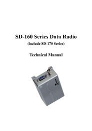
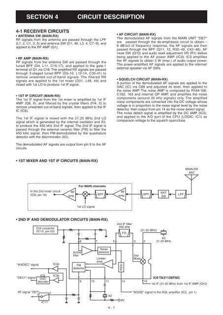
SECTION 4.CIRCUIT DESCRIPTION4-1 RECEIVER CIRCUITS• ANTENNA SW (MAIN-RX)RF signals from the antenna are passed through the LPF(L1, 2, C1, 3, 5) and antenna SW (D1, 46, L3, 4, C7~9), andapplied to the RF AMP (Q1).• RF AMP (MAIN-RX)RF signals from the antenna SW are passed through thetuned BPF (D4, L11, C15-17), and applied to the gate-1terminal of Q1 via C18. The amplifi ed RX signals are passedthrough 3-staged tuned BPF (D5-10, L12-14, C30-41) toremove unwanted out-of-band signals. The filtered RXsignals are applied to the 1st mixer (D21, L48, 49) andmixed with 1st LO to produce 1st IF signal.• 1ST IF CIRCUIT (MAIN-RX)The 1st IF signal from the 1st mixer is amplified by 1st IFAMP (Q8, 9), and filtered by the crystal filters (FI4, 5) toremove unwanted out-of-band signals, then applied to the IF<strong>IC</strong> (<strong>IC</strong>6).The 1st IF signal is mixed with the 21.25 MHz 2nd LOsignal which is generated by the internal oscillator and X3,to produce the 450 kHz 2nd IF signal. The 2nd IF signal ispassed through the external ceramic fi lter (FI6) to fi lter the450 kHz signal, then FM-demodulated by the quadraturedetector with the discriminator (X2).• AF CIRCUIT (MAIN-RX)The demodulated AF signals from the MAIN UNIT "DET"are passed through the de-emphassis circuit to obtain –6 dB/oct of frequency response, the AF signals are thenpassed through the BPF (Q11, 12, R32–40, C42–46), AFmute SW (Q13) and audio level adjustment VR (R1) beforebeing applied to the AF power AMP (<strong>IC</strong>3). <strong>IC</strong>3 amplifiesthe AF signals to obtain 5 W (max.) of audio output power.The power-amplifi ed AF signals are applied to the internal/external speaker via AF SWs.• SQUELCH CIRCUIT (MAIN-RX)A portion of the demodulated AF signals are applied to theDAC (<strong>IC</strong>) via C89 and adjusted its level, then applied tothe noise AMP. The noise AMP is composed by R164-166,C162, 163 and internal OP AMP, and amplifies the noisecomponents (around 30 kHz signals) only. The amplifiednoise components are converted into the DC voltage whosevoltage is in proportion to the noise signal level by the noisedetector, then output from pin 14 as the noise detect signal.The noise detect signal is amplifi ed by the DC AMP (<strong>IC</strong>2),and applied to the A/D port of the CPU (LOG<strong>IC</strong>; <strong>IC</strong>1) ascomparison voltage to the squelch open/close.The demodulated AF signals are output from pin 9 to the AFcircuits.• 1ST MIXER AND 1ST IF CIRCUITS (MAIN-RX)MAIN-RXANTFor MAIN channelsto the 2nd mixer circuit(<strong>IC</strong>6, pin 16)RFamp.BPFRFamp.BPFANTSWLPF1st LO signal• 2ND IF AND DEMODULATOR CIRCUITS (MAIN-RX)D/A convertor(<strong>IC</strong>15, pin 23)2nd IF filter450 kHzFI38 7 5 3(21.25 MHz)2X321.25 MHz"WXDEC" signal<strong>IC</strong>3aActivefilterFMdetectorNoisedetectorLimiteramp.RSSI2ndMixer<strong>IC</strong>9"DEC1" signal DSCdecoder<strong>IC</strong>3b910111416<strong>IC</strong>6 TA31136FNG1st IF (31.05 MHz) from 1st IF AMP (Q10)AF signal "DET"1<strong>IC</strong>117X28V"NOISE" signal to the SQL amplifier (<strong>IC</strong>2, pin 1)4 - 1