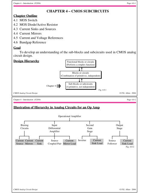
CHAPTER 4 – CMOS SUBCIRCUITS - Analog IC Design.org
CHAPTER 4 – CMOS SUBCIRCUITS - Analog IC Design.org
CHAPTER 4 – CMOS SUBCIRCUITS - Analog IC Design.org

You also want an ePaper? Increase the reach of your titles
YUMPU automatically turns print PDFs into web optimized ePapers that Google loves.
Chapter 4 – Section 1 (5/2/04) Page 4.1-9Influence of the OFF State on MOS SwitchesThe OFF state influence is primarily in any current that flows from the terminals of theswitch to ground.An example might be:v in++R C-Bulk H- v CHFig. 4.1-10Typically, no problems occur unless capacitance voltages are held for a long time. Forexample,v out (t) = v CH e-t/(R Bulk C H )If R Bulk ≈ 109Ω and C H = 10pF, the time constant is 109·10-11 = 0.01secondsv out<strong>CMOS</strong> <strong>Analog</strong> Circuit <strong>Design</strong> © P.E. Allen - 2004Chapter 4 – Section 1 (5/2/04) Page 4.1-10Influence of Parasitic CapacitancesThe parasitic capacitors have two influences:• Parasitics to ground at the switch terminals (C BD and C BS ) add to the value of thedesired capacitors.This problem is solved by the use of stray-insensitive switched capacitor circuits• Parasitics from gate to source and drain cause charge injection onto or off the desiredcapacitors.This problem can be minimized but not eliminated.Model for studying charge injection:1 C channelC 1channelC channel122CGS0CGD0CGS0CGD0C L +R channelC L +R channel C L +V v S CL Vv CLSV v S CL---A simple switch circuit usefulfor studying charge injection.A distributed model ofthe transistor switch.A lumped model ofthe transistor switch.Fig. 4.1-11<strong>CMOS</strong> <strong>Analog</strong> Circuit <strong>Design</strong> © P.E. Allen - 2004
Chapter 4 – Section 1 (5/2/04) Page 4.1-11Charge Injection (Clock feedthrough, Charge feedthrough)Charge injection is a complex analysis which is better suited for computer analysis.Here we will attempt to develop an understanding sufficient to show ways of reducing theeffect of charge injection.What is Charge Injection?1.) When the voltages change across the gate-drainand gate-source capacitors, a current will flowbecause i = C dvdt .2.) When the switch is off, charge injection willappear on the external capacitors (C L ) connected toFig. 4.1-12the switch terminals causing their voltages to change.There are two cases of charge injection depending upon the transition rate when theswitch turns off.1.) Slow transition time.2.) Fast transition time.<strong>CMOS</strong> <strong>Analog</strong> Circuit <strong>Design</strong> © P.E. Allen - 2004Chapter 4 – Section 1 (5/2/04) Page 4.1-12Slow Transition TimeConsider the following switch circuit:ABSwitch ONv in +V TCSwitch OFFABCv in +V TChargeinjectionv inFig. 4.1-13C Lv inC L1.) During the on-to-off transition time from A to B, the charge injection is absorbed bythe low impedance source, v in .2.) The switch turns off when the gate voltage is v in +V T (point B).3.) From B to C the switch is off but the gate voltage is changing. As a result chargeinjection occurs to C L .<strong>CMOS</strong> <strong>Analog</strong> Circuit <strong>Design</strong> © P.E. Allen - 2004
Chapter 4 – Section 1 (5/2/04) Page 4.1-13Fast Transition TimeFor the fast transition time, the rate of transition is faster than the channel time constantso that some of the charge during the region from point A to point B is injected onto C Leven though the transistor switch has not yet turned off.ABSwitch ONv in +V TCSwitch OFFABCv in +V TChargeinjectionC Lv inChargeinjectionC Lv in Fig. 4.1-14<strong>CMOS</strong> <strong>Analog</strong> Circuit <strong>Design</strong> © P.E. Allen - 2004Chapter 4 – Section 1 (5/2/04) Page 4.1-14A Quantized Model of Charge Injection †Approximate the gate transition as a stair case and discretize in voltage as follows:VoltageVoltageDiscretized Gate VoltageDiscretized Gate Voltagev GATEv GATEChargev in +V Tv in +V Tinjectionv inv indue to fastv CLv CLtransitionttSlow TransitionFast TransitionThe time constant of the channel, R channel·C channel , determines whether or not thecapacitance, C L , fully charges during each voltage step.Fig 4.1-15†B.J. Sheu and C. Hu, “Switched-Induced Error Voltage on A Switched Capacitor,” IEEE J. Solid-State Circuits, Vol. SC-19, No. 4, pp. 519-525,August 1984.<strong>CMOS</strong> <strong>Analog</strong> Circuit <strong>Design</strong> © P.E. Allen - 2004
Chapter 4 – Section 1 (5/2/04) Page 4.1-15Analytical Expressions to Approximate Charge InjectionAssume the gate voltage is making a transition from high, V H , to low, V L .∴ v Gate = v G (t) = V H - Utwhere U = magnitude of the slope of v G (t)Define V HT = V H - V S - V T and β = K’WL .The error in voltage across C L , V error , is given below in two terms. The first termcorrsponds to the feedthrough that occurs while the switch is still on and the second termcorresponds to feedthrough when the switch is off.1.) Slow transition occurs when βV 2HT2C L>> U.⎜ ⎜⎛ W·CGD0 + C channel2V error = - ⎝ C ⎠ ⎟⎟⎞ πUC LL2β - W·CGD0C L(V S +2V T -V L )2.) Fast transition occurs when βV 2HT2C L
Chapter 4 – Section 1 (5/2/04) Page 4.1-17Example 4.1-2 - Calculation of Charge Feedthrough ErrorCalculate the effect of charge feedthrough v Gon the previous circuit where V S = 1V, C L 5V= 200fF, W/L = 0.8µm/0.8µm, and V G isgiven below for the two cases. Use modelCase 2parameters from Tables 3.1-2 and 3.2-1.Case 1Neglect ∆L and ∆W effects.0VtSolution0.2nsCase 1:10nsFig. 4.1-17The value of U is equal to 5V/0.2nS or 25x109. Next we must test to see if the slowor fast transition time is appropriate. First calculate the value of V T asV T = V T0 + γ 2|φ F | -V BS - γ 2|φ F | = 0.7 + 0.4 0.7+1 - 0.4 0.7 = 0.887VTherefore,V HT =V H -V S -V T = 5-1-0.887=3.113V ⇒ βV 2HT2C = 110x10-6·3.1132L 2·200fF = 2.66x10⁹ < 25x109which corresponds to the fast transition case. Using the previous expression gives,V error =-⎜ ⎛ 176x10-18+0.5(1.58x10⁻¹⁵)⎝ 200x10-15 ⎠ ⎟⎞⎝ ⎜⎛ 3.113- 3.32x10 -330x10-3 ⎠ ⎟⎞ - 176x10 -18(1+1.774-0) = -16.94mV200x10-15<strong>CMOS</strong> <strong>Analog</strong> Circuit <strong>Design</strong> © P.E. Allen - 2004Chapter 4 – Section 1 (5/2/04) Page 4.1-18Example 4.1-2- ContinuedCase 2:In this case U is equal to 5V/10ns or 5x10⁸ which means that the slow transition caseis valid (5x10⁸ < 2.66x10⁹).Using the previous expression gives,V error = -⎜ ⎛ 176x10-18+0.5(1.58x10⁻¹⁵)⎝ 200x10-15 ⎠ ⎟⎞⎝ ⎜⎜⎛ 314x10-6220x10-6⎠ ⎟⎟⎞ -176x10 -18(1+1.774-0) = -8.21mV200x10-15Comment:These results are not expected to give precise answers regarding the amount ofcharge feedthrough one should expect in an actual circuit. Rather, they are a guide tounderstand the effects of various circuit elements and terminal conditions in order tominimize unwanted behavior by design techniques.<strong>CMOS</strong> <strong>Analog</strong> Circuit <strong>Design</strong> © P.E. Allen - 2004
Chapter 4 – Section 1 (5/2/04) Page 4.1-19Solutions to Charge Injection1.) Use minimum size switches to reduce the overlap capacitances and/or increaseC L .2.) Use a dummy compensating transistor.φ 1 φ 1W 1L 1M1W DL D= W 12L 1MDFig. 4.1-19• Requires complementary clocks• Complete cancellation is difficult and may in fact may make the feedthrough worse3.) Use complementary switches (transmission gates)4.) Use differential implementation of switched capacitor circuits (probably the bestsolution)<strong>CMOS</strong> <strong>Analog</strong> Circuit <strong>Design</strong> © P.E. Allen - 2004Chapter 4 – Section 1 (5/2/04) Page 4.1-20Input-Dependent Charge InjectionExamination of the error voltage reveals that,Error voltage = Component independent of input + Component dependent on inputThis only occurs for switches that are floating and is due to the fact that the inputinfluences the voltage at which the transistor switches (v in ≈ V S ≈ V D ). Leads tospurious responses and other undesired results.Solution:φ 1Use delayed clocks toCremove the input-dependenceby breaking theφ 1diC s φ 2φ 2Vincurrent path for injectionS1 S4V outφ φfrom the floating switches.2 S2 S3 1C Lttφ 1dClock DelayAssume that C s is chargedto V in (both φ 1 and φ 1dare high):1.) φ 1 opens, no input-dependent feedthrough because switch terminals (S3) are atground potential.2.) φ 1d opens, no feedthrough occurs because there is no current path (except throughsmall parasitic capacitors).tFig. 4.1-20<strong>CMOS</strong> <strong>Analog</strong> Circuit <strong>Design</strong> © P.E. Allen - 2004
Chapter 4 – Section 1 (5/2/04) Page 4.1-21<strong>CMOS</strong> Switches (Transmission Gate)ClockAV DDBAClockBClockClockAdvantages:• Feedthrough somewhat diminished• Larger dynamic range• Lower ON resistanceDisadvantages:• Requires a complementary clock• Requires more areaFig. 4.1-21<strong>CMOS</strong> <strong>Analog</strong> Circuit <strong>Design</strong> © P.E. Allen - 2004Chapter 4 – Section 1 (5/2/04) Page 4.1-22Example 4.1-3 - Charge Injection for a <strong>CMOS</strong> SwitchCalculate the effect of charge feedthrough on thecircuit shown below. Assume that U = 5V/50ns =10 8 V/s, v in = 2.5V and ignore the bulk effect. Usethe model parameters from Tables 3.1-2 and 3.2-1.Solutionv inFirst we must identify the transition behavior. Forthe NMOS transistor we haveβ N V 2HTN2C L= 110x10 -6·(5-2.5-0.7)2= 1.78x10 82·10-12For the PMOS transistor, noting thatV HTP = V S - |V TP | - V L = 2.5-0.7-0 = 1.80.8µm0.8µm0.8µm0.8µmwe have β PV 2HTP2C L= 50x10 -6·(1.8)2= 8.10x102·10-12 7 . Thus, the NMOS transistor is in theslow transition and the PMOS transistor is in the fast transition regimes.Error due to NMOS:V error (NMOS) = -⎜ ⎛ 176x10-18 + 0.5(1.58x10⁻¹⁵)⎝ 10-12⎠ ⎟⎞ π·108·10-122·110x10-6 - 176x10 -18(2.5+1.4-0)10-12= -1.840mV<strong>CMOS</strong> <strong>Analog</strong> Circuit <strong>Design</strong> © P.E. Allen - 20045V0VM2M15V0VC L =1pF+v CL-v in -|V TP |v in +V TNFig. 4.1-18
Chapter 4 – Section 1 (5/2/04) Page 4.1-23Example 4.1-3 - ContinuedError due to PMOS:V error (PMOS) = ⎜ ⎛ 176x10-18+0.5(1.58x10⁻¹⁵)⎝ 10-12 ⎠ ⎟⎞⎝ ⎜⎛ 1.8- 50x10 -6(1.8)36·108·10-12 ⎠ ⎟⎞ +176x10 -18(5+1.4-2.5)10-12= 1.956mVNet error voltage due to charge injection is 116µV. This will vary with V S .<strong>CMOS</strong> <strong>Analog</strong> Circuit <strong>Design</strong> © P.E. Allen - 2004Chapter 4 – Section 1 (5/2/04) Page 4.1-24Dynamic Range of the <strong>CMOS</strong> SwitchThe dynamic range of a switch is therange of voltages at the switchterminals (V A ≈V B =V A,B ) over whichthe ON resistance stays reasonablysmall.AM1V DDV DDV A,B 1µAM2Fig. 4.1-22Spice File:Simulation <strong>CMOS</strong> transmission switch resistanceM1 1 3 2 0 MNMOS L=1U W=10UM2 1 0 2 3 MPMOS L=1U W=10U.MODEL MNMOS NMOS VTO=0.7, KP=110U,+LAMBDA=0.04, GAMMA=0.4, PHI=0.7.MODEL MPMOS PMOS VTO=-0.7, KP=50U,+ LAMBDA=0.05, GAMMA=0.5, PHI=0.8BSwitch On Resistance10kΩ8kΩ6kΩV DD =2V4kΩV DD=2V2kΩV DD =2.5VV DD =3V00V 0.5V 1V 1.5V 2V 2.5V 3VV A,B (Common mode voltage) Fig. 4.1-22AVDD 3 0VAB 1 0IA 2 0 DC 1U.DC VAB 0 3 0.02 VDD 1 3 0.5.PRINT DC V(1,2).ENDResult:Low ON resistance over a wide voltage range is difficult as the power supply decreases.<strong>CMOS</strong> <strong>Analog</strong> Circuit <strong>Design</strong> © P.E. Allen - 2004V DD=1VV DD=1.5VV DD =1VV DD =1.5V
Chapter 4 – Section 1 (5/2/04) Page 4.1-25<strong>CMOS</strong> Switch with Twin-Well SwitchingV ControlM1V DD<strong>Analog</strong>SignalInputM3M4M5<strong>Analog</strong>SignalOutputV SSM2V ControlCircuit when V Control is in its high state.High StateCircuit when V Control is in its low state.Low StateM1M1<strong>Analog</strong>SignalInput<strong>Analog</strong>SignalOutput<strong>Analog</strong>SignalInputV SSV DD<strong>Analog</strong>SignalOutputM2M2Low StateHigh State<strong>CMOS</strong> <strong>Analog</strong> Circuit <strong>Design</strong> © P.E. Allen - 2004Chapter 4 – Section 1 (5/2/04) Page 4.1-26Charge Pumps for Switches with Low Power Supply VoltagesAs power supply voltages decrease below 3V, it becomes difficult to keep the switchon at a low value of on-resistance over the range of the power supply. Consequently,charge pumps are used.Charge pump circuit:V DD = 3.3VC 1 C 2(Prevents latchup)V sub_hiM10VC LTo asingleNMOSswitchV hi ≈ 5V0V3.3V0VC 2V hi = 2V DD·C gate,NMOS switch + C 2 + C L<strong>CMOS</strong> <strong>Analog</strong> Circuit <strong>Design</strong> © P.E. Allen - 2004
Chapter 4 – Section 1 (5/2/04) Page 4.1-27Charge Pump - ContinuedHigh voltage generator for the well of M1:V DD =3.3V6.6VV sub_hi3.3VC1C2C BulkC Storage0VFig. 4.1-225Prevents latch-up of M1 by providing a high bulk bias (6.6V).Use a separate clock driver for each switch to avoid crosstalk through the gate clocklines. Area for layout can be small.<strong>CMOS</strong> <strong>Analog</strong> Circuit <strong>Design</strong> © P.E. Allen - 2004Chapter 4 – Section 1 (5/2/04) Page 4.1-28Simulation of the Charge Pump Circuit †Circuit:CLK_outM5M1M2M3V DDCLK_outCLK_inM6C 1C 1M4Simulation:3.0OutputV SSFig. 4.1-232.0InputVolts1.00.0-1.0 0.0 1.0 2.0 3.0 4.0 5.0 6.0 7.0 8.0 9.0 10.0Time (µs)Fig. 4.1-24†T.B. Cho and R.R. Gray, “A 10b, 20 Msample/s, 35mW Pipeline A/D Converter,” IEEE J. of Solid-State Circuits, Vol. 30, No. 3m March 1995, pp.166-172.<strong>CMOS</strong> <strong>Analog</strong> Circuit <strong>Design</strong> © P.E. Allen - 2004
Chapter 4 – Section 2 (5/2/04) Page 4.2-3Application of the MOS DiodeDC resistor:DC resistance = v i ⎪ Q = V I• Useful for biasing - creating current from voltageand vice versaiI DV DSAC ResistanceDC ResistanceSmall-Signal Load (AC resistance):V TvFig. 4-2-2BGDSBGDSBG+v gs-SB+v bs-g m v gsg mbs v bsAC resistance = v ds 1i =1d g m + g ≈ ds g mwhereg m = β(V GS -V T ) = 2βI D and g ds ≈ β 2 (V GS-V T )2 λ = ID λr dsi dD+v ds-SFig. 4.2-4<strong>CMOS</strong> <strong>Analog</strong> Circuit <strong>Design</strong> © P.E. Allen - 2004Chapter 4 – Section 2 (5/2/04) Page 4.2-4Influence of the Back Gate (Bulk)It can be shown that the small signal model for the MOSFET with the bulk not connectedto the source is,whereGDSBGDSBG+v gs-SB+v bs-g m v gsg mbs v bsg mbs is defined as ∂ι D ⎪ ⎛ ∂i⎜ D⎞⎛∂v ⎟⎜GS⎞⎪⎟∂v BS Q = ⎪⎜ ⎟ ⎝∂v GS⎜ ⎟⎠ ⎝∂v BS ⎠Q = ⎜ ⎜ ⎛⎝ ⎠ ⎟ ⎟- ∂i D⎞ ⎛ ∂v⎜ T⎞⎪∂v T⎜ ⎝ ⎠⎟⎟ ⎪∂v BS Qg m γg mbs == ηg2 2|φF| - V m BSr dsi dD+v ds-SFig. 4.2-4It is very useful to simplify the small signal model when possible. The following arereasonable guidelines for this simplification:g m ≈ 10g mbs ≈ 100g ds<strong>CMOS</strong> <strong>Analog</strong> Circuit <strong>Design</strong> © P.E. Allen - 2004
Chapter 4 – Section 2 (5/2/04) Page 4.2-5Example 4.2-1 - Small-Signal Load ResistanceFind the small signal resistance of the MOS diodeshown using the parameters of Table 3.2-1.Assume that the W/L ratio is 10µm/1µm.SolutionIf we are going to include the bulk effect, we must first findthe dc value of the bulk-source voltage. Unfortunately, we do notknow the threshold voltage because the bulk-source voltage isunknown. The best approach is to ignore the bulk-source voltage,find the gate-source voltage and then iterate if necessary.V DD = 5V100µA2I2·100∴ V GS = β + V T0 = 110·10 + 0.7 = 1.126VThus let us guess at a gate-source voltage of 1.3V (to account for the bulk effect) andcalculate the resulting gate-source voltage.V T = V T0 +γ 2|φF|-(-3.7)-γ 2|φF| = 0.7+0.4 0.7+3.7-0.4 0.7 = 1.20V ⇒ V GS = 1.63VNow refine our guess at V GS as 1.6V and repeat the above to get V T = 1.175V whichgives V GS = 1.60V.Therefore, V BS = -3.4V.r acFig. 4.2-5<strong>CMOS</strong> <strong>Analog</strong> Circuit <strong>Design</strong> © P.E. Allen - 2004Chapter 4 – Section 2 (5/2/04) Page 4.2-6Example 4.2-1 - ContinuedThe small signal model for this example is shown.The ac input resistance is found by,i ac = g ds v ac - g m v gs - g mbs v bs= g ds v ac + g m v s + g mbs v s = v ac (g m +g mbs +g ds )v ac 1∴ r ac = i = ac g m +g mbs +g dsNow we must find the parameters which are,i d G,D,Br acg m v gs g mbs v bs+r ds v ds = v gsv ac-Si ac Fig. 4.2-6g m = 2βI D = 2·110·10·100 µS = 469µS, g ds = 0.04V-1·100µA = 4µS,and g mbs = 469µS·0.4 = 0.0987·469µS = 46.33µS2 0.7+3.4106Finally, r ac = 469 + 46.33 + 4 = 1926ΩIf we had used the previous approximations of g m ≈ 10g mbs ≈ 100g ds , then we could havesimply letr ac ≈ 1/g m = 1/469µS = 2132ΩProbably the most important result of this approximation is that we would not have tofind V BS which took a lot of effort for little return.<strong>CMOS</strong> <strong>Analog</strong> Circuit <strong>Design</strong> © P.E. Allen - 2004
Chapter 4 – Section 2 (5/2/04) Page 4.2-7Applications of the MOS Diode for Biasing1.) Deriving a bias voltage from power supply.I D1 = I D2 ⇒ βN(V Bias -V TN )2 = βP(V DD -V Bias -|V TP |)2Solving for V Bias givesV TN +V Bias =βPβN (V DD-|V TP |)1 +βPβNand I D = βN(V Bias -V TN )2Use the ratio of βP/βN to design V Bias and the value of βN to designthe current I D .M2M1V DD+I DV Bias-Fig. 4.2-72.) Deriving a bias voltage from a bias current.V Bias = V GS1 + V GS2I BiasM2V DD+2I Bias 2I Bias= β1+ V T1 + β2+ V T2<strong>Design</strong> β1 and β2 to yield the desired value of V Bias . Try to keepthe values of W/L as close to unity as possible to minimize area.M1VBias-Fig. 4.2-8<strong>CMOS</strong> <strong>Analog</strong> Circuit <strong>Design</strong> © P.E. Allen - 2004Chapter 4 – Section 2 (5/2/04) Page 4.2-8Use of the MOSFET to Implement a Floating ResistorIn many applications, it is useful to implement aresistance using a MOSFET. First, consider thesimple, single MOSFET implementation.LR AB = K’W(V GS - V T )100µA60µA20µAV GS =8VV GS =7VV GS =10VV GS =9VV BiasA B A R AB BFig. 4.2-9V GS =2V-20µAV GS =3VV GS =4V-60µAV GS =5VV GS =6V-100µA-1V -0.6V -0.2V 0.2V 0.6V 1VFig. 4.2-95<strong>CMOS</strong> <strong>Analog</strong> Circuit <strong>Design</strong> © P.E. Allen - 2004
Chapter 4 – Section 2 (5/2/04) Page 4.2-9Cancellation of Second-Order Voltage Dependence – Parallel MOSFETsCircuit:V DD VDDi AB+ -I BiasIBias++M1i AB V CV CA -B A R AB BM2-+ -v ABv ABFig. 4.2-10Assume both devices are non-saturated⎡i D1 = ß 1⎢⎣(v AB + V C - V T )v AB - v AB 2 ⎤2⎡i D2 = ß 2⎢⎣(V C - V T )v AB - v AB 2 ⎤2⎡i AB = i D1 + i D2 = ß ⎢⎣v AB2 + (V C - V T )v AB - v AB 2i AB = 2ß(V C - V T )v AB1R AB = 2ß(V C - V T )⎥⎦⎥⎦2 + (V C - V T )v AB - v AB 22<strong>CMOS</strong> <strong>Analog</strong> Circuit <strong>Design</strong> © P.E. Allen - 2004⎤⎥⎦Chapter 4 – Section 2 (5/2/04) Page 4.2-10Parallel MOSFET PerformanceVoltage-Current Characteristic:I(VSENSE)2mA1mA0W=15uL=3uVBS=-5.0VVc=7V6V5V4V3V-1mA-2mA-2 -1 0 1 2SP<strong>IC</strong>E Input File:NMOS parallel transistor realizationM1 2 1 0 5 MNMOS W=15U L=3UM2 2 4 0 5 MNMOS W=15U L=3U.MODEL MNMOS NMOS VTO=0.75, KP=25U,+LAMBDA=0.01, GAMMA=0.8 PHI=0.6VC 1 2E1 4 0 1 2 1.0VSENSE 10 2 DC 0Still have the influence of the bulk on the threshold voltage.VDSFig. 4.1-11VDS 10 0VSS 5 0 DC -5.DC VDS -2.0 2.0 .2 VC 3 7 1.PRINT DC I(VSENSE).PROBE.END<strong>CMOS</strong> <strong>Analog</strong> Circuit <strong>Design</strong> © P.E. Allen - 2004
Chapter 4 – Section 2 (5/2/04) Page 4.2-11Double MOSFET Differential ResistorCancels the bulk effect.v 1R i 1v 2R i 2-+V C1i D1M1i 1v 1i D2 V SSM2-vV C2i +D3 M3vi D4 V SSi 2v 2M4Fig. 4.2-12V C1i D1 = β [(V C1 -v-V T )(v 1 -v) - 0.5(v 1 -v) 2 ] i D2 = β [(V C2 -v-V T )(v 1 -v) - 0.5(v 1 -v) 2 ]i D3 = β [(V C2 -v-V T )(v 2 -v) - 0.5(v 2 -v) 2 ] i D4 = β [(V C1 -v-V T )(v 2 -v) - 0.5(v 2 -v) 2 ]i 1 = i D1 +i D3 = β [(V C1 -v-V T )V 1 -v) - 0.5(v 1 -v) 2 + (V C2 -v-V T )(v 2 -v) - 0.5(v 2 -v) 2 ]i 2 = i D2 +i D4 = β [(V C2 -v-V T )(v 1 -v) - 0.5(v 1 -v) 2 + (V C1 -v-V T )(v 2 -v) - 0.5(v 2 -v) 2 ]i 1 - i 2 = β [(V C1 -v-V T )(v 1 -v) + (V C2 -v-V T )(v 2 -v) + (V C2 -v-V T )(v 1 -v) + (V C1 -v-V T )(v 2 -v)]= β [v 1 (V C1 -V C2 ) + v 2 (V C2 -V C1 )] = β (V C1 -V C2 )(v 1 -v 2 )Differential input resistance isR in = v 1-v 2 v 1 -v 2i 1 -i 2= β (V C1 -V C2 )(v 1 -v 2 ) = 1β (V C1 -V C2 ) , v 1,v 2 ≤ min{(V C1 -V T ),(V C2 -V T )}<strong>CMOS</strong> <strong>Analog</strong> Circuit <strong>Design</strong> © P.E. Allen - 2004Chapter 4 – Section 2 (5/2/04) Page 4.2-12Double-MOSFET, Differential Resistor Performance150uA100uA50uAI(VSENSE)0- 50uA-100uA-150uAVBC =-5VV3 =0VVC1 =7VVC2 =6V5V4V3V2V-3 -2 -1 0 1 2V 1 -V 2SP<strong>IC</strong>E Input File:Double MOSFET Differential Resistor RealizationM1 1 2 3 4 MNMOS1 W=3U L=3UM2 1 5 8 4 MNMOS1 W=3U L=3UM3 6 5 3 4 MNMOS1 W=3U L=3UM4 6 2 8 4 MNMOS1 W=3U L=3UVSENSE 3 8 DC 0VC1 2 0 DC 7VVC2 5 0VSS 4 0 DC -5VV12 1 6.MODEL MNMOS1 NMOS VTO=0.75 KP=25U+LAMBDA=0.01 GAMMA=0.8 PHI=0.6.DC V12 -3 3 0.2 VC2 2 6 1.PRINT DC I(VSENSE)).PROBE.ENDComments:• Good linearity and tunability.• Can be used as a multiplier.<strong>CMOS</strong> <strong>Analog</strong> Circuit <strong>Design</strong> © P.E. Allen - 2004
Chapter 4 – Section 2 (5/2/04) Page 4.2-13Summary of Active Resistor RealizationsAC ResistanceRealizationLinearity HowControlledRestrictionsSingle MOSFET Poor V GS or v BULK < Min (v S , v D )W/LParallel MOSFET Good V C or W/L v ≤ (V C - V T )Double-MOSFET,differential resistorVeryGoodV C1 - V C2orW/Lv 1 , v 2 < min(V C1 -V T ,V C2 -V T )v BULK < min(v 1 ,v 2 )Transresistance only<strong>CMOS</strong> <strong>Analog</strong> Circuit <strong>Design</strong> © P.E. Allen - 2004Chapter 4 – Section 3 (5/2/04) Page 4.3-1SECTION 4.3 - CURRENT SINKS AND SOURCESCharacterization of MOS Sinks and SourcesA sink/source is characterized by two quantities:• r out - a measure of the “flatness” of the current sink/source (its independence ofvoltage)• V MIN - the min. across the sink or source for which the current is no longer constant<strong>CMOS</strong> Current Sink:r out =V DDV GGi OUT+v OUT-1di D /dv DS= 1+λV DSλΙD ≈ 1λI Di OUTV MIN;;;;;; V GG -V T0andVMIN = V DS (sat) = V GS - V T0 = V GG - V T000Slope = 1/r outV GGv OUTV DDFig. 4.3-1<strong>CMOS</strong> <strong>Analog</strong> Circuit <strong>Design</strong> © P.E. Allen - 2004
Chapter 4 – Section 3 (5/2/04) Page 4.3-2Simple MOS Current SourceV DDV GG+i OUT vOUT-i OUTV DD -V GGSlope = 1/r out0 0This current source only works when v OUT ≤ V GG + |V T0 |V MINV GG;;;;;;v OUTV GG +|V T0 | V DDFig. 280-02<strong>CMOS</strong> <strong>Analog</strong> Circuit <strong>Design</strong> © P.E. Allen - 2004Chapter 4 – Section 3 (5/2/04) Page 4.3-3Gate-Source Voltage ComponentsIt is important to note that the gate-source voltage consists of two parts as illustratedbelow:i D10W/LW/L0.1W/LI DV GSv GSEnhanceChannelProvideCurrent00V TFig. 280-03V GS = V T0 + V ON = Part to enhance the channel + Part to cause current flowwhereV ON = V DS (sat) = V GS - V T0∴ V MIN = V ON = V DS (sat) =2I DK’(W/L)for the simple current sink.Note that V MIN can be reduced by using large values of W/L.<strong>CMOS</strong> <strong>Analog</strong> Circuit <strong>Design</strong> © P.E. Allen - 2004
Chapter 4 – Section 3 (5/2/04) Page 4.3-4Simulation of a Simple MOS Current SinkiOUT (µA)120;;;;;0;10080604020Slope = 1/R outV minV GS1 =1.126V10µm1µmi OUT+v OUT-0 1 2 3 4 5v OUT (Volts)Comments:V MIN is too large - desire V MIN to approach zero, at least approach V CE (sat)Slope too high - desire the characteristic to be flat implying very large output resistance(K N ’ = 110µA/V2, V T = 0.7Vand λ = 0.04V-1) ⇒ r ds = 250kΩ<strong>CMOS</strong> <strong>Analog</strong> Circuit <strong>Design</strong> © P.E. Allen - 2004Chapter 4 – Section 3 (5/2/04) Page 4.3-5Increasing the Output Resistance of a Current Sink/SourcePrinciple:In order to increase the output resistance, use negative series feedback because,r out (with feedback) = r out (without feedback) x [1 + Loop gain]Circuit:i OUT How does it work?+ 1.) Assume i out increases.+M2v GS2.) As a result, v S increases.- + vV OUTGGR v S 3.) Since the gate is held constant at V GG , then v GS decreases.- -4.) The decrease in v GS causes i OUT to decrease opposing theFig. 280-08original increaseLoop Gain?M2'i OUT 'V GGRi OUT+M2+v S-v OUT-Fig. 280-09i OUTi OUT ’ = g m v S = g m Ri OUT∴ Loop gain = i OUT’i OUT= g m Rr out (w.fb.) = r out (w/o fb.)x [1+g m R] = r ds (1+g m R)If g m R >>1, then r out (w. fb.) ≈ g m r ds R<strong>CMOS</strong> <strong>Analog</strong> Circuit <strong>Design</strong> © P.E. Allen - 2004
Chapter 4 – Section 3 (5/2/04) Page 4.3-6Increasing the Output Resistance of a Simple MOS Current SinkSmall signal model for calculating thei OUToutput resistance for the cascodeM2 +current sink:g m v gs2g mbs v bs2r ds2i out+Loop equation:v out = (i out -g m2 v gs2 -g mbs2 v bs2 )r ds2+ i out RV GGRv OUT-Rv g2 = v b2 = 0+v outv s2--Fig. 280-10= i out (r ds2 +R) - g m2 r ds2 v gs2 - g mbs2 r ds2 v bs2But,vgs2 = 0 - v s2 = -i out R and v bs2 = 0 - v s2 = -i out RTherefore,v out = i out [r ds2 + R + g m2 r ds2 R + g mbs2 r ds2 R]orr out = v outi out= r ds2 + R + g m2 r ds2 R + g mbs2 r ds2 R ≈ g m2 r ds2 R = µ 2 R (µ = g m r ds )A general principle emerges:The output resistance of a cascode circuit ≈ R x (Common source voltage gain of thecascoding transistor)<strong>CMOS</strong> <strong>Analog</strong> Circuit <strong>Design</strong> © P.E. Allen - 2004Chapter 4 – Section 3 (5/2/04) Page 4.3-7MOS Cascode Current Sinkds2V GG2+V GG1v s2M1 v OUTv outM2 + g m2 v gs2 g mbs2 v bs2 ri OUTi out+g m1 v gs1 r ds1-v gs1 =v g2 = v b2 = 0- -Fig. 280-11Small signal output resistance:Noting that v gs1 = v g2 = v b2 = 0 and writing a loop equation we get,v out = (i out - g m2 v gs2 - g mbs2 v bs2 )r ds2 + r ds1 i outHowever,v gs2 = 0 - v s2 = -i out r ds1 and v bs2 = 0 - v s2 = -i out r ds1Therefore,v out = i out [r ds1 + r ds2 + g m2 r ds1 r ds2 + g mbs2 r ds1 r ds2 ]orr out = v outi out= r ds1 + r ds2 + g m2 r ds1 r ds2 + g mbs2 r ds1 r ds2 ≈ g m2 r ds1 r ds2 = µ 2 r ds1Comments:1.) Same as before if R = r ds1 2.) Bulk effects have little influence.<strong>CMOS</strong> <strong>Analog</strong> Circuit <strong>Design</strong> © P.E. Allen - 2004
Chapter 4 – Section 3 (5/2/04) Page 4.3-8Simulation of the Cascode <strong>CMOS</strong> Current SinkExampleUse the model parametersK N ’=110µA/V2, V T = 0.7 and λN =0.04V-1 to calculate (a) the smallsignaloutput resistance for the simplecurrent sink if I OUT = 100µA and (b)the small-signal output resistance forthe cascode current sink with I OUT =100µA. Assume that all W/L valuesare 1.iOUT (µA)120;;;;;;;;;;0;;10080604020V GG2 =1.552VV GG1 =1.126VV minSlope = 1/R outAll W/Ls are10µm/1µmi OUT+0 1 2 3 4 5v OUT (Volts)Fig. 280-12Solution(a) Using λ = 0.04 V-1 and I OUT = 100µA gives r ds1 = 250kΩ = r ds2 . (b) Ignoring thebulk effect, we find that g m1 = g m2 = 469µS which gives r out = (250kΩ)(469µS)(250kΩ)= 29.32MΩ.v OUT-<strong>CMOS</strong> <strong>Analog</strong> Circuit <strong>Design</strong> © P.E. Allen - 2004Chapter 4 – Section 3 (5/2/04) Page 4.3-9Gate-Source Matching PrincipleA. If the gate-source voltages of two or more transistorsare equal and the transistors are matched and operatingin the saturation region, then the currents are related bythe W/L ratios of the individual transistors. The gatesourcevoltages may be directly connected or implied.i D1 = K’W 12L (v 1 GS1 -V T1 )2 → (v GS1 -V T1 )2 = 2K’i D1(W 1 /L 1 )i D2 = K’W 22L 2(v GS2 -V T2 )2 → (v GS2 -V T2 )2 = 2K’i D2(W 2 /L 2 )If v GS1 = v GS2 , thenW 2⎞ ⎛W ⎟ ⎜ 1⎞⎛W ⎟⎜ 1 /L 1⎞⎟L 2⎟ i⎠ D1 = ⎜ ⎟ ⎝L 1i⎠ D2 or i D1 = ⎜ ⎟⎝W 2 /L 2i⎠ D2⎛⎜⎜⎝B. If the drain currents of two or more transistors are equal and the transistorsare matched and operating in the saturation region, then the gatesourcevoltages are related by the W/L ratios (ignoring bulk effects).If i D1 = i D2 , then v GS1 = V T1 +W 2 /L 2W 1 /L 1(v GS2 - V T2 )i D1i D2M1 M2W 1W 2L 1+ + L 2v GS1 v GS2--Fig. 290-02W 1+ L 1v GS1-i D2M2W 2+ L 2v GS2-Fig. 290-03orif W 2 /L 2 = W 1 /L 1 , then v GS1 = v GS2 (Note: V DS1 must equal V DS2 for ideal results)<strong>CMOS</strong> <strong>Analog</strong> Circuit <strong>Design</strong> © P.E. Allen - 2004i D1
Chapter 4 – Section 3 (5/2/04) Page 4.3-10Practical Cascode Current Sink ImplementationDoes not require any batteries and uses the gate-source matching principle.V DDi OUTI REF 2V T +2V ONi OUTM2 + +M4v+ + DS2V T +V ON V T +V ON--- v OUT+M3 + V T +V ONV T +V ON -- M1 -v OUT0V T +2V ONFig. 4.3-10However, V MIN is now equal to V T +V ON + v DS2 (min) = V T + V ON + V ON = V T + 2V ONAssuming that I OUT = 100µA and W 2 /L 2 = W 1 /L 1 = 10 gives V ON = 0.426V.Thus V MIN = 0.7V + 2·0.426V = 1.55V (this is way too much)<strong>CMOS</strong> <strong>Analog</strong> Circuit <strong>Design</strong> © P.E. Allen - 2004Chapter 4 – Section 3 (5/2/04) Page 4.3-11High-Swing Cascode Current SinkSince2I DV ON = K’(W/L) ,then if L/W isquadrupled, thenV ON is doubled.∴ V MIN = 2V ON .V DDV DDI REF I REFi OUTM4M2 +1/1+1/4V++ ONV T +V ON-vV OUTT +2V-ON M3 M1 +1/1 + V ON-V T +V ON 1/1 ---i OUTV MIN0 2V ONv OUTFig. 290-04ExampleUse the cascode current sink configuration above to design a current sink of 100µAand a V MIN = 1V. Assume the device parameters of Table 3.1-2.SolutionWith V MIN = 1V, choose V ON = 0.5V. Assuming M1 and M2 are identical givesWL = 2·I OUTK’·V ON2 = 2·100x10-6110x10-6x0.25 = 7.27 ⇒ W 1L = W 21 L = W 32 L = 7.27 and W 43 L = 1.82 4<strong>CMOS</strong> <strong>Analog</strong> Circuit <strong>Design</strong> © P.E. Allen - 2004
Chapter 4 – Section 3 (5/2/04) Page 4.3-12Improved High-Swing Cascode Current SinkBecause the drain-source voltages ofthe matching transistors, M1 and M3are not equal, i OUT ≠ I REF .V DDV DDTo circumvent this problem the cascodecurrent sink shown is utilized:Note that the drain-source voltage ofM1 and M3 are identical causing i OUTto be a replication of I REF .<strong>Design</strong> Procedure1.) Since V MIN = 2V ON = 2V DS (sat), let V ON = 0.5V MIN .2I REF2.) V ON = K’(W/L) ⇒ W 1L = W 21 L = W 32 L = W 53 L = 2I REF53.) W 4L 4=2I REFK’(V GS4 -V T )2 =2I REFK’(2V ON )2 =I REF I REFi OUT+M4 M5 M2 +V 1/1+1/4TV++ ON- 1/1V T +V ON -+-M3 M1 + v OUTV T +2V ONV ON + V ON1/1 V T +V ON 1/1- - - - -I REF2K’V ON2Fig. 290-05K’V ON2 = 8I REFK’V MIN2<strong>CMOS</strong> <strong>Analog</strong> Circuit <strong>Design</strong> © P.E. Allen - 2004Chapter 4 – Section 3 (5/2/04) Page 4.3-13Signal Flow in TransistorsThe last example brings up an interesting and important point. This point is illustratedby the following question, “How does I REF flow into the M3-M5 combination oftransistors since there is no path to the gate of M5?”Consider how signals flow in transistors:InputOnly+G+Output OnlyD- ++S+InputOnly+B+Output OnlyC- ++E+Fig. 4.3-12BAnswer to the above question:As V DD increases (i.e. the circuit begins to operate),I REF cannot flow into the drain of M5, so it flows throughthe path indicated by the arrow to the gate of M3. Itcharges the stray capacitance and causes the gate-sourcevoltage of M3 to increase to the exact value necessary tocause I REF to flow through the M3-M5 combination.I REFV DDM5M3+V GS3-V T +2V ONFig. 4.3-12A<strong>CMOS</strong> <strong>Analog</strong> Circuit <strong>Design</strong> © P.E. Allen - 2004
Chapter 4 – Section 3 (5/2/04) Page 4.3-14Example 4.3-1 - <strong>Design</strong> of a Minimum V MIN Current SinkAssume I REF = 100µA and design a cascode current sink with a V MIN = 0.3V using thefollowing parameters: VTO=0.7, KP=110U, LAMBDA=0.04, GAMMA=0.4, PHI=0.7SolutionFrom the previous equations, we getW 1L 1= W 2L 2= W 3L 3= W 5L 5=W 4L 4=I REF2K’V ON2 = 1002·110·0.152 = 20.2Simulation Results:Low Vmin Cascade Current Sink - Method No. 2M1 5 1 0 0 MNMOS W=81U L=1UM2 2 3 5 5 MNMOS W=81U L=1UM3 4 1 0 0 MNMOS W=81U L=1UM4 3 3 0 0 MNMOS W=20U L=1UM5 1 3 4 4 MNMOS W=81U L=1U.MODEL MNMOS NMOS VTO=0.7 KP=110U+LAMBDA=0.04 GAMMA=0.4 PHI=0.7VDD 6 0 DC 5VIIN1 6 1 DC 100UIIN2 6 3 DC 100UVOUT 2 0 DC 5.0.OP.DC VOUT 5 0 0.05.PRINT DC ID(M2).END8I REFK’V MIN2 = 8·100110·(0.3V)2 = 80.8 andiOUT(µA)<strong>CMOS</strong> <strong>Analog</strong> Circuit <strong>Design</strong> © P.E. Allen - 2004120100806040200V MIN0 1 2 3 4 5v OUT (V)Fig. 290-06Chapter 4 – Section 3 (5/2/04) Page 4.3-15Self-Biased Cascode Current Sink †The V T + 2V ON bias voltage is developed through a seriesresistor.<strong>Design</strong> procedure:Same as the previous exceptR = V ONI REF= V MIN2I REFFor the previous example,0.3VR = 2·100µA = 1.5kΩI REF+V DDV T +2V ONRV ON- VT +V ON+ M3 M4i OU-+ M1 M2 +V ONV ONV T--Fig. 290-0Observation:Note that the last several slides have been devoted to just getting the MOS cascodecurrent sink/source to have the same minimum voltage as the BJT!†T.L. Brooks and A.L. Westwick, “A Low-Power Differential <strong>CMOS</strong> Bandgap Reference,” Proc. of IEEE Inter. Solid-State Circuits Conf., Feb.1994, pp. 248-249.<strong>CMOS</strong> <strong>Analog</strong> Circuit <strong>Design</strong> © P.E. Allen - 2004
Chapter 4 – Section 3 (5/2/04) Page 4.3-16MOS Regulated Cascode Sink †I REFM7M6V DDM5i OUTV GS3 (max)Increasing v GS3I REF+I REF V GS3 (norm)AM3V O1vM4OUTM1M2-v DS3V DS3 (min) V DS3 (sat)Fig. 290-08Comments:• Achieves very high output resistance by increasing the loop gain due to the M4-M5inverting amplifier.⎛⎜Loop gain = g m3 r ds2⎝ ⎜g m4⎞⎟⎟⎠g ds4 +g ds5≈ g m3r ds2 g m4 r ds42 if r ds4 ≈ r ds5 ∴ r out ≈ r ds3g m3 r ds2 g m4 r ds42• M3 maintains “constant” current even though it is no longer in the saturation region.Assume an i OUT increase → v S3 increase → v GS4 increase→ v G3 decrease → Large decrease in v GS3 → Large decrease in i OUTi D3† E. Sackinger and W. Guggenbuhl, “A Versatile Building Block: The <strong>CMOS</strong> Differential Difference Amplifier,” IEEE J. of Solid-State Circuits, vol.SC-22, no. 2, pp. 287-294, April 1987.<strong>CMOS</strong> <strong>Analog</strong> Circuit <strong>Design</strong> © P.E. Allen - 2004Chapter 4 – Section 3 (5/2/04) Page 4.3-17Regulated Cascode Current Sink - ContinuedSmall signal model:Solving for the output resistance:i out = g m3 v gs3 + g ds3 (v out -v gs4 )Butvgs4 = i out r ds2D2=S3=G3=D4=D5+ v gs3G4 g m3 v-gs3+r ds5 r ds4rds2v gs4g m4 v gs4r ds3-S2 = G2= S4andvgs3 = v g3 - v s3 = -g m4 (r ds4 ||r ds5 )v gs4 - v gs4 = -r ds2 [1 + g m4 (r ds4 ||r ds5 )]i outi outD3 +v out-Fig. 290-09∴i out = -g m3 r ds2 [1 + g m4 (r ds4 ||r ds5 )]i out + g ds3 v out - g ds3 r ds2 i outv out = r ds3 [1 + g m3 r ds2 + g ds3 r ds2 + g m3 r ds2 g m4 (r ds4 ||r ds5 )]i out∴ r out = v outi out= r ds3 [1 + g m3 r ds2 + g ds3 r ds2 + g m3 r ds2 g m4 (r ds4 ||r ds5 )]≈ r ds3 g m3 r ds2 g m4 (r ds4 ||r ds5 )If I REF = 100µA, all W/Ls are 10µm/1µm we get r ds = 0.25MΩ and g m = 469µS whichgivesr out ≈ (0.25MΩ)(469µS)(0.25MΩ)(469µS)(0.125MΩ) = 1.72GΩ<strong>CMOS</strong> <strong>Analog</strong> Circuit <strong>Design</strong> © P.E. Allen - 2004
Chapter 4 – Section 3 (5/2/04) Page 4.3-18Regulated Cascode Current Sink - ContinuedV MIN :Without the use of the V O1 battery shown, V MIN is pretty bad. It is,V MIN = V GS4 + V DS3 (sat) = V T + 2V ONMinimizing V MIN :If V O1 = V T , then V MIN = 2V ON . This is accomplished by the following circuit:V DD V DD V DDI REF+I BI D4A I Bi OUTM3 + +V DS2M4A M4B -+ +V GS4A V GS4BI Bv OUTM1- -M2I REF +I B+V DS2If V GS4A - V GS4B = V DS2 (sat) = V ON ,then V MIN = 2V ON∴2I D4K N ’(W 4A /L 4A ) -2I BK N ’(W 4B /L 4B ) =2I B +2I REK N ’(W 2 /L- - orFig. 290-10I D4 I B I B +I REFW 4A /L 4A- W 4B /L 4B= W 2 /L 2A number of solutions exist. For example, let I B = I REF . This gives I D4A = 5.824I REFassuming all W/L ratios are identical.<strong>CMOS</strong> <strong>Analog</strong> Circuit <strong>Design</strong> © P.E. Allen - 2004Chapter 4 – Section 3 (5/2/04) Page 4.3-19Example 4.3-4 - <strong>Design</strong> of a Minimum V MIN Regulated Cascode Current Sink<strong>Design</strong> a regulated cascode current sink for 100µA and minimum voltage of V MIN = 0.3V.SolutionLet the W/L ratios of M1 through M5 be equal and let I B = 10µA. Therefore,V MIN = 0.3V = V ON3 + V ON2 ==2·100µA110µA/V2(W/L) ⎝ ⎛1 + 1.1⎠⎞Therefore,2·100µA0.3V =110µA/V2(W/L) (2.049)WL = 2·100µA·2.049 2= 84.8 ≈ 85.110µA/V20.32With I B = 10µA, then I D4A =⎛⎝⎞10 + 110 2 ⎠ = 186µA2·100µA110µA/V2(W/L)+M185/12·110µA110µA/V2(W/L)+5V +5V +5V110µA 186µA 10µA i OUTM3 +85/1M4A M4B85/1 85/110µA v OUTM2110µA85/1-Fig. 290-11<strong>CMOS</strong> <strong>Analog</strong> Circuit <strong>Design</strong> © P.E. Allen - 2004
Chapter 4 – Section 3 (5/2/04) Page 4.3-20Comparison of the MOS Cascode Current Sink and Regulated Cascode CurrentSinkClose examination in the knee area reveals interesting differences.Simulation results:110iOUT (µA)1051009590RegulatedMOSCascodeMOS CascodeBJT Cascode85800 0.1 0.2 0.3 0.4 0.5v OUT (V)Fig. 290-12Comments:• The regulated cascode current is smaller than the cascode current because the drainsourcevoltages of M1 and M2 are not equal.• The regulated cascode current sink has a smaller V MIN due to the fact that M3 canhave a drain-source voltage smaller than V DS (sat).<strong>CMOS</strong> <strong>Analog</strong> Circuit <strong>Design</strong> © P.E. Allen - 2004Chapter 4 – Section 3 (5/2/04) Page 4.3-21Summary of Current Sinks and SourcesCurrent Sink/Source r OUT V MINSimple MOS Current Sinkr ds = λΙ 1V D DS (sat) =V ONSimple BJT Current Sinkr o = V AV CE (sat)ΙC≈ 0.2VCascode MOS ≈ g m2 r ds2 r ds1 V T + 2V ONCascode BJT ≈ β F r o 2V CE (sat)Minimum V MIN Cascode Current ≈ g m2 r ds2 r ds12V ONSinkRegulated Cascode Current Sink* ≈ r ds3 g m3 r ds2 g m4 (r ds4 ||r ds5 ) ≈ V T +V ONMinimum V MIN RegulatedCascode Current Sink*≈ r ds3 g m3 r ds2 g m4 (r ds4 ||r ds5 ) ≈V ON* Unfortunately, the regulated cascode current sink has a dominant pole in the feedbackloop which can cause a pole-zero doublet which leads to a combination of fast and slowtime constants. For this reason, the regulated cascode circuit should only be used inbiasing applications unless the impact of this dynamic is understood.<strong>CMOS</strong> <strong>Analog</strong> Circuit <strong>Design</strong> © P.E. Allen - 2004
Chapter 4 – Section 4 (5/2/04) Page 4.4-1SECTION 4.4 - CURRENT MIRRORSCharacterization of Current MirrorsA current mirror is basically nothing more than a current amplifier. The idealcharacteristics of a current amplifier are:• Output current linearly related to the input current, i out = A i i in• Input resistance is zero• Output resistance is infinityAlso, the characteristic V MIN applies not only to the output but also the input.• V MIN (in) is the range of v in over which the input resistance is not small• V MIN (out) is the range of v out over which the output resistance is not largeGraphically:i outi inV MIN (in)i in i out+v Current+in v out- Mirror -i out= 1/R inSlopeSlope = 1/R out1i in voutv inA iV MIN (out)Fig. 300-01Input Characteristics Transfer Characteristics Output CharacteristicsTherefore, R out , R in , V MIN (out), V MIN (in), and A i will characterize the current mirror.<strong>CMOS</strong> <strong>Analog</strong> Circuit <strong>Design</strong> © P.E. Allen - 2004Chapter 4 – Section 4 (5/2/04) Page 4.4-2Simple MOS Current Mirrori Ii O+ M1 M2 +v DS1 + v DS2- vGS - --Fig. 300-02Assume that v DS2 > v GS - V T2 , theni OiI⎛L ⎜ 1 W 2⎞⎛V ⎟⎜GS -V T2⎞ ⎡1 + λv= ⎜ ⎟ ⎝W 1 L 2⎜⎠ ⎝ ⎠⎟⎟ ⎢ DS2⎛K ⎤⎜ 2 ’⎞⎟⎥V GS -V T1⎢⎥2⎣1 + λv DS1⎜ ⎟ ⎝K 1 ’⎠⎦If the transistors are matched, then K 1 ’ = K 2 ’ and V T1 = V T2 to give,i O⎛L ⎜ 1 W 2⎞⎛1 + λv⎟⎜DS2⎞⎟i = I⎜ ⎟ ⎝W 1 L 2⎜⎟⎠ ⎝1 + λv DS1 ⎠If v DS1 = v DS2 , theni OiI⎛L ⎜ 1 W 2⎞⎟= ⎜ ⎟ ⎝W 1 L 2 ⎠Therefore the sources of error are 1.) v DS1 ≠ v DS2 and 2.) M1 and M2 are not matched.<strong>CMOS</strong> <strong>Analog</strong> Circuit <strong>Design</strong> © P.E. Allen - 2004
Chapter 4 – Section 4 (5/2/04) Page 4.4-3Influence of the Channel Modulation Parameter, λIf the transistors are matched and the W/L ratios are equal, theni Oi I= 1 + λv DS21 + λv DS1if the channel modulation parameter is the same for both transistors (L 1 = L 2 ).Ratio error (%) versus drain voltage difference:8.0λ = 0.02Note that one could use this effect tomeasure λ.1 ⎤⎥ × 100 %⎦7.06.0Ratio Error v DS2 - v DS1 (volts)λ = 0.015Measure V DS1 ,V DS2 , i I and i O andsolve the above equation for the channelmodulation parameter, λ.λ v DS2−λ v DS1++11Ratio Error ⎡⎢⎣5.04.03.02.0λ = 0.011.0v DS1 = 2.0 volt0.00.0 1.0 2.0 3.0 4.0 5.0Fig. 300-03v DS2 - v DS1 (volts)<strong>CMOS</strong> <strong>Analog</strong> Circuit <strong>Design</strong> © P.E. Allen - 2004Chapter 4 – Section 4 (5/2/04) Page 4.4-4Influence of Mismatched TransistorsAssume that v DS1 = v DS2 and that K 1 ’ ≠ K 2 ’ and V T1 ≠ V T2 . Therefore we havei Oi I= K 2’(v GS - V T2 )2K 1 ’(v GS - V T1 )2How do you analyze the mismatch? Use plus and minus worst case approach. Define∆K’ = K’ 2 -K’ 1 and K’ = 0.5(K 2 ’+K 1 ’) ⇒ K 1 ’= K’-0.5∆K’ and K 2 ’= K’+0.5∆K’∆V T = V T2 -V T1 and V T = 0.5(V T1 +V T2 ) ⇒ V T1 =V T -0.5∆V T and V T2 =V T +0.5∆V TSubstituting these terms into the above equation gives,⎛i OiI= (K’+0.5∆K’)(v GS - V T - 0.5∆V T )2(K’-0.5∆K’)(v GS - V T + 0.5∆V T )2 = ⎝ ⎜1 + ∆K’⎞ ⎛ ∆V⎟⎜ T⎞2⎟2K’ ⎠⎜1 -⎟⎝2(v GS -V T )⎠⎛⎜1 - ∆K’⎞ ⎛ ∆V⎟⎜ T⎞2⎟⎝ 2K’ ⎠⎜1 +⎟⎝2(v GS -V T )⎠Assuming that the terms added to or subtracted from “1” are smaller than unity givesi O ⎛i ≈⎜I ⎝1 + ∆K’⎞ ⎛⎟⎜2K’ 1 + ∆K’⎞ ⎛ ∆V⎟⎜ T⎞2⎛∆V⎟ ⎜ T⎞2 ∆K’⎟⎠⎝2K’ ⎠⎜1 -⎟⎝2(v GS -V T ) ⎜1 -⎟⎠ ⎝2(v GS -V T ) ≈ 1 +⎠K’ - 2∆V T(v GS -V T )Assume ∆K’/K’ = ±5% and ∆V T /(v GS -V T ) = ±10%.∴ i O /i I ≈ 1 ± 0.05 ±(-0.20) = 1 ± (0.25) ⇒ ±15% error if tolerances are correlated.<strong>CMOS</strong> <strong>Analog</strong> Circuit <strong>Design</strong> © P.E. Allen - 2004
Chapter 4 – Section 4 (5/2/04) Page 4.4-5Illustration of the Offset Voltage Error InfluenceAssume that V T1 = 0.7V and K’W/L = 110µA/V2.16.0i I = 1µARatio Error ⎡ i O ⎤⎢ − 100⎣ i 1 ⎥ × %i ⎦14.012.010.08.06.04.0i I = 3µAi I = 5µAi I = 10µA2.0i I = 100µA0.00.0 1.0 2.0 3.0 4.0 5.0 6.0 7.0 8.0 9.0 10∆V T (mV)Fig. 300-4Key: Make the part of V GS causing the current to flow, V ON , more significant than V T .<strong>CMOS</strong> <strong>Analog</strong> Circuit <strong>Design</strong> © P.E. Allen - 2004Chapter 4 – Section 4 (5/2/04) Page 4.4-6Influence of Error in Aspect Ratio of the TransistorsExample 1 - Aspect Ratio Errors in Current MirrorsFigure 4.4-4 shows the layout of a one-to-four current amplifier. Assume that the lengthsare identical (L 1 = L 2 ) and find the ratio error if W 1 = 5 ± 0.1 µm. The actual widths of thetwo transistors areW 1 = 5 ± 0.1 µm and W 2 = 20 ± 0.1 µmi OM2i Oi IM1iGND;;;;;;;;;;+V DS1-IM1V GS+-M2+V DS2-Fig. 300-5SolutionWe note that the tolerance is not multiplied by the nominal gain factor of 4. The ratio ofW 2 to W 1 and consequently the gain of the current amplifier isi O W 2 20 ± 0.1iI = W = 1 5 ± 0.1 = 4 ⎛1 ± (0.1/20)⎞⎜⎟⎝ 1 ± (0.1/5) ≈ 4 ⎛⎜1 ± 0.1⎞ ⎛⎟⎜⎠ ⎝ 20 ⎠ ⎝1 - ±0.1⎞⎟5 ≈ 4 ⎛⎞⎜1 ± 0.1⎟⎠ ⎝ 20 - ±0.420 = 4 - (±0.03)⎠where we have assumed that the variations would both have the same sign (correlated). Itis seen that this ratio error is 0.75% of the desired current ratio or gain.<strong>CMOS</strong> <strong>Analog</strong> Circuit <strong>Design</strong> © P.E. Allen - 2004
Chapter 4 – Section 4 (5/2/04) Page 4.4-7Influence of Error in Aspect Ratio of the Transistors-ContinuedExample 2 - Reduction of the Aspect Ratio Errors in Current MirrorsUse the layout technique illustrated in Fig. 4.4-5 and calculate the ratio error of a currentamplifier having the specifications of the previous example.SolutionsThe actual widths of M1 and M2 areW 1 = 5 ± 0.1 µm and W 2 = 4(5 ± 0.1) µmThe ratio of W 2 to W 1 and consequently the current gain is given below and is for allpractical purposes independent of layout error.i O 4(5 ± 0.1)iI = 5 ± 0.1 = 4M2aM2b M1M2c;; ;; ;;;;; ;; ;;;;; ;;GND;;;;; ;; ;;;i Ii OM2di Ii OM1M2GNDFig. 300-6;;;;<strong>CMOS</strong> <strong>Analog</strong> Circuit <strong>Design</strong> © P.E. Allen - 2004Chapter 4 – Section 4 (5/2/04) Page 4.4-8Summary of the Simple MOS Current Mirror/Amplifier• Minimum input voltage is V MIN (in) = V T +V ONOkay, but could be reduced to V ON .Principle:M5 M6M7V DDIVI bM3 M4i IV TiO+V TM1+ M1V ON +ON + M2- V T +V ON- V T +V- ON-I bM2I bbi Oi IFig. 300-7Will deal with later in low voltage op amps.• Minimum output voltage is V MIN (out) = V ON• Output resistance is R out = 1λI D• Input resistance is R in ≈ 1g m• Current gain accuracy is poor because v DS1 ≠ v DS2<strong>CMOS</strong> <strong>Analog</strong> Circuit <strong>Design</strong> © P.E. Allen - 2004
Chapter 4 – Section 4 (5/2/04) Page 4.4-9MOS Cascode Current MirrorImproving the output resistance:i IM3M1iOM4M2D3=G3=G4D4+++g m3 v 3 r ds3 v 3r ds4g m4 v gs4S3=G2 -S4iin v inv outg m1 v 1D1=G1r ds1+v 1D2r ds2- S1 -g m2 v gs2S2 -i outFig. 310-018• R out :v out = r ds4 (i out -g m4 v gs4 ) + r ds2 (i out -g m2 v gs2 )But, i in = 0 so that v 1 = v 3 = 0 ⇒ v gs4 = -v s4 = -i out r ds2 and v gs2 = 0∴ v out = i out [r ds4 + r ds2 + g m4 r ds2 r ds4 ] ≈ r ds2 g m4 r ds4• R in :R in =1g m3||r ds3 +1g m1||r ds1 ≈1g m1+1 2g ≈ m3 g m• V MIN (out) = V T + 2V ON• V MIN (in) = 2(V T +V ON )• Current gain match: Excellent since v DS1 = v DS2<strong>CMOS</strong> <strong>Analog</strong> Circuit <strong>Design</strong> © P.E. Allen - 2004Chapter 4 – Section 4 (5/2/04) Page 4.4-10Large Output Swing Cascode Current MirrorV DDV DDI REF I I IOi i1/11/4M4M5M2V DDi o1/1+g m5 v gs5D5=G3r ds5M31/1M11/1v inD3=S5 +g m3 v gs3r ds3 v s5= g m3v in- S3=G5 -Fig. 310-02• R out ≈ g m2 r ds2 r ds1• R in = ?v in = r ds5 (i in -g m5 v gs5 )+v s5 = r ds5 (i in + g m5 v s5 )+v s5 = r ds5 i in +(1+g m5 r ds5 )v s5But, v s5 = r ds3 (i in - g m3 v in )∴v in = r ds5 i in + (1+g m5 r ds5 )r ds3 i in - g m3 r ds3 (1+g m5 r ds5 )v inR in = v ini in= r ds5 + r ds3 + r ds3 g m5 r ds5 1g m3 r ds3 (1+g m5 r ds5 ) ≈ g m3• V MIN (out) = 2V ON• V MIN (in) = V T + V ON• Current gain is excellent because v DS1 = v DS3 .<strong>CMOS</strong> <strong>Analog</strong> Circuit <strong>Design</strong> © P.E. Allen - 2004iin
Chapter 4 – Section 4 (5/2/04) Page 4.4-11Self-Biased Cascode Current MirrorV DDV DDi inI 1 I 2i out+Rg m3 v gs3• R in = ?+ +M3 M4v in = i in R + r ds3 (i in -g m3 v gs3 )v in r ds3v in v 2++ r ds1 (i in -g m1 v gs1 )M1 M2g m1 v gs1 v 1-But,-- -v gs1 = v in -i in RSelf-biased, cascode current mirror Small-signal model to calculate R in .Fig. 310-03andvgs3 = v in -r ds1 (i in -g m1 v gs1 ) = v in -r ds1 i in +g m1 r ds1 (v in -i in R)∴ v in = i in R+r ds3 i in -g m3 r ds3 [v in -r ds1 i in +g m1 r ds1 (v in -i in R)]+r ds1 [i in -g m1 (v in +i in R)]v in [1+g m3 r ds3 +g m1 r ds1 g m3 r ds3 +g m1 r ds1 ]= i in [R+r ds1 +r ds3 +g m3 r ds3 r ds1 + g m1 r ds1 g m3 r ds3 R]R + r ds1 + r ds3 + g m3 r ds3 r ds1 + g m1 r ds1 g m3 r ds3 R 1R in = 1 + g m3 r ds3 + g m1 r ds1 g m3 r ds3 + g m1 r ≈ ds1 g m1+ R• R out ≈ g m4 r ds4 r ds2• V MIN (in) = V T + 2V ON •V MIN (out) = 2V ON • Current gain matching is excellent<strong>CMOS</strong> <strong>Analog</strong> Circuit <strong>Design</strong> © P.E. Allen - 2004i inRrds1Chapter 4 – Section 4 (5/2/04) Page 4.4-12Wilson MOS Current Mirrori IM1iOM3M2i out+g m3 v gs3 r ds3i in+ v v gs3 -out++v in g m1 v gs1 r ds1 g m2 v gs2 r ds2 v gs2 =v gs1Uses negative series feedback to achieve higher output resistance.• R out = ? (i in =0)v gs2 =-v out = r ds2 (i out - g m3 v gs3 ) + v gs2- -Fig. 310-09i out r ds2 i outg m2 +g = ds2 1+g m2 r and v ds2 gs3 = -g m1 r ds1 v gs2 - v gs2 = -(1+g m1 r ds1 )v gs2∴ v out = r ds2 i out + g m3 r ds2 (1+g m1 r ds1 )v gs2 = i out ⎣⎢ ⎢⎡ r ds3 +r ds2⎝ ⎜ ⎜⎛1+g m3r ds2 +g m1 r ds1 g m3 r ds31 + g m2 r ds2⎛1+g ⎜ m3 r ds2 +g m1 r ds1 g m3 r ds3⎞⎟R out = r ds3 +r g m1r ds1 g m3 r ds3ds2⎝ ⎜ 1 + g m2 r ds2⎟ ≈⎠g m2<strong>CMOS</strong> <strong>Analog</strong> Circuit <strong>Design</strong> © P.E. Allen - 2004
Chapter 4 – Section 4 (5/2/04) Page 4.4-13Wilson Current Mirror - Continued• R in = ? (v out = 0)i in ≈ g m1 v gs1 =g m1 g m3 v gs3g m2 +g ds2 +g ds3≈ g m1g m3 v gs3g m2v gs3 = v in - v gs1 = v in - g m1g m3 v gs3g m2⇒ v gs3 =∴ i g m1g m3 v inin ≈ g m2 +g ⇒ m3R in = g m2 +g m3g m1 g m3• V MIN (in) = 2(V T +V ON )• V MIN (out) = V T + 2V ON• Current gain matching - poor, v DS1 ≠ v DS2v in1 + g m1g m3g m2<strong>CMOS</strong> <strong>Analog</strong> Circuit <strong>Design</strong> © P.E. Allen - 2004Chapter 4 – Section 4 (5/2/04) Page 4.4-14Evolution of the Regulated Cascode Current Mirror from the Wilson CurrentMirrori Ii OM3i Ii OM3M1M1M2V Bias2M2Wilson Current Mirror RedrawnRegulated Cascode Current SinkFig. 310-10<strong>CMOS</strong> <strong>Analog</strong> Circuit <strong>Design</strong> © P.E. Allen - 2004
Chapter 4 – Section 4 (5/2/04) Page 4.4-15MOS Regulated Cascode Current MirroriII iV DDI BiasV DDIOV DDi oM3M1M4M2• R out ≈ g m 2r ds3FIG. 310-111• R in ≈ g m4• V MIN (out) = V T +2V ON (Can be reduced to 2V ON )• V MIN (in) = V T +V ON (Can be reduced to V ON )• Current gain matching - good as long as v DS4 = v DS2<strong>CMOS</strong> <strong>Analog</strong> Circuit <strong>Design</strong> © P.E. Allen - 2004Chapter 4 – Section 4 (5/2/04) Page 4.4-16SUMMARYSummary of MOS Current MirrorsCurrentMirrorAccuracyOutputResistanceInputResistanceMinimumOutputVoltageMinimumInputVoltageSimple Poor r ds1g mV ON V T +V ONCascode Excellent g m r ds2Wide OutputSwingCascodeSelf-biasedCascodeExcellent g m r ds22g mV T +2V ON 2(V T +V ON )1g m2V ON V T +V ONExcellent g m r ds2 R + 1g m2V ON V T +2V ONWilson Poor g m r ds2RegulatedCascodeGood-Excellentg m 2r ds3 1g m2g m2(V T +V ON ) V T +2V ONV T +2V ON(min. is2V ON )V T +V ON(min. isV ON )<strong>CMOS</strong> <strong>Analog</strong> Circuit <strong>Design</strong> © P.E. Allen - 2004
Chapter 4 – Section 5 (5/2/04) Page 4.5-1SECTION 4.5 - CURRENT AND VOLTAGE REFERENCESCharacteristics of a Voltage or Current ReferenceWhat is a Voltage or Current Reference?A voltage or current reference is an independent voltage or current source that has ahigh degree of precision and stability.Requirements of a Reference Circuit:• Should be independent of power supply• Should be independent of temperature• Should be independent of processing variations• Should be independent of noise and other interferenceReferenceNominalValueNoiseTemperaturePower SupplyFig. 4.5-1<strong>CMOS</strong> <strong>Analog</strong> Circuit <strong>Design</strong> © P.E. Allen - 2004Chapter 4 – Section 5 (5/2/04) Page 4.5-2REFERENCES WITH POWER SUPPLY INDEPENDENCEPower Supply IndependenceHow do you characterize power supply independence?Use the concept of:S I REFV= ∂I REF/I REFDD ∂V DD /V DD= V DD⎛∂I ⎜ REF⎞⎟I REF⎜ ⎟ ⎝∂V DD ⎠Application of sensitivity to determining power supply dependence:∂I REFI REF= ⎜ ⎛⎝ S I REFV ⎠ ⎟⎞ ∂V DDDDV DDThus, the fractional change in the reference voltage is equal to the sensitivity times thefractional change in the power supply voltage.For example, if the sensitivity is 1, then a 10% change in V DD will cause a 10% change inI REF .Ideally, we want S I REFV DDto be zero for power supply independence.<strong>CMOS</strong> <strong>Analog</strong> Circuit <strong>Design</strong> © P.E. Allen - 2004
Chapter 4 – Section 5 (5/2/04) Page 4.5-3Simple Current ReferenceV CCRV DDI INI INRI OUTI D1I OUTI C1I B1 I B2Q1Q2M1M2Fig. 360-02I OUT ≈ V CC-V BE ⎛ 1 ⎞⎜ ⎟R ⎜ ⎟⎝1+ 2 I OUT ≈ V DD-V GSV DD -R =β F ⎠R2I INβ 1- V TS I REFV= 1 CCTemperature and process dependence?S I REFV DD= 1<strong>CMOS</strong> <strong>Analog</strong> Circuit <strong>Design</strong> © P.E. Allen - 2004Chapter 4 – Section 5 (5/2/04) Page 4.5-4MOS Widlar Current ReferenceOperation:V GS1 – V GS2 – I OUT R 2 = 0I OUT R 2 + V ON2 – V ON1 = 0Assuming strong inversion and λ → 0,2I OUTI OUT R 2 + K'(W 2 /L 2 ) – V ON1 = 0Solving for I OUT gives,2- K'(W 2 /L 2 ) + 2K'(W 2 /L 2 ) + 4R 2V ON1I OUT =2R 22I INwhere V ON1 = K'(W 1 /L 1 )Differentiating I OUT with respect to V DD gives,1 dI OUT1dV ON12 I OUT dV DD=2/(K' W 2 /L 2 )+ 4R 2 V ON1 dV DD,∴S I REFV DD=S I OUTV DD=V ON1V ON2 2+4 I OUT R 2 V ON1S I INV DD≈I INI D1dV ON1dV DDV DDR 1M1= V ON12I INM2dI INdV DDV ON14V ON1 2 S I INV DD= 0.5S I INV DDI OUTR 2Fig. 360-04<strong>CMOS</strong> <strong>Analog</strong> Circuit <strong>Design</strong> © P.E. Allen - 2004
Chapter 4 – Section 5 (5/2/04) Page 4.5-5Example 4.5-1For the MOS Widlar current reference, find I OUT if I IN = 100µA, R 2 = 4kΩ, K’ =200µA/V 2 , and W 2 /L 2 = W 1 /L 1 = 25. Assume the temperature is 27°C and that n = 1.5.Find the sensitivity of I OUT with respect to V DD .SolutionV ON1 =-I OUT =2I INK'(W 1 /L 1 ) = 2·100200·25 = 0.2V2200·25 + 2200·25 + 4(0.004)0.220.004 µA = 5 µA ⇒ I OUT = 25µANote that V ON2 = V ON1 - I OUT R 2 = 0.2-(25)(0.004) = 0.1V > 2nV t = 78mV so bothtransistors are in strong inversion.For the sensitivity calculations, assume that V DD >> V GS1 . Therefore I IN ≈ V DD /R 1 .S I REF V ON1V= DD 4V S I IN V ON1ON2 2 V≈ DD 4V ON2 2 = 0.5Therefore, a 10% variation in V DD causes a 5% variation in I OUT .<strong>CMOS</strong> <strong>Analog</strong> Circuit <strong>Design</strong> © P.E. Allen - 2004Chapter 4 – Section 5 (5/2/04) Page 4.5-6MOS Peaking Current ReferenceVStrong Inversion Operation:Circuit:DDV GS1 – I IN R – V GS2 = 0I INV ON2 = V ON1 – I IN RI OUT = K'(W R2/L 2 )I OUT2 V ON22= K'(W M1M22/L 2 )2 (V ON1 – I IN R) 2whereTransfer Characteristics:2I IN1.6V ON1 = K'(W 1 /L 1 )1.4Weak Inversion Operation:1.2I INV GS2 – V T ≈ nV t ln ⎜⎛1.0⎜ ⎝(W 1 /L 1 )I T ⎠ ⎟⎟⎞ – I IN RI OUT (µA)0.80.6If the transistors are identical and V DS2 > 3V T ,I OUT = W 0.41 V GS2 – V T -I IN RL 1I T exp ⎜⎛⎜ ⎝nV t≈ I IN exp ⎜⎛ ⎜ ⎝nV t ⎠ ⎟⎟⎞0.2 Strong Inversion⎠ ⎟⎟⎞Fig. 360-72 4 6 8 10I IN (µA)Fig. 360-8<strong>CMOS</strong> <strong>Analog</strong> Circuit <strong>Design</strong> © P.E. Allen - 200400Weak Inversion
Chapter 4 – Section 5 (5/2/04) Page 4.5-7Threshold Referenced Current ReferenceCircuit:Operation:I OUT = V VGS1 T +R 2=2I INK'(W 1 /L 1 )R 2≈ V TR 2if V T > V ON1The sensitivity of I OUT with respect to V DD isS I OUT ⎛ V⎜ ON1V = ⎜DD ⎝I OUT R 2⎞⎟⎟⎠S I IN ⎛ V⎜ ON1V = ⎜DD ⎝2V GS1⎞⎟⎟⎠S I INV DDFor example, if V T = 1V, V ON1 = 0.1V and S I INV DD≈ 1, thenV DDR 1S I OUT ⎛ 0.1 ⎞V= ⎜ ⎟DD ⎝ 2·1.1 = 0.045⎠Therefore, if V DD changes by 10%, I REF or I OUT changes by 0.45%.<strong>CMOS</strong> <strong>Analog</strong> Circuit <strong>Design</strong> © P.E. Allen - 2004I INI D1M1M2I OUTR 2Fig. 360-10Chapter 4 – Section 5 (5/2/04) Page 4.5-8SIMPLE BIAS/REFERENCE CIRCUITSVoltage References using Voltage DivisionV DDR 1V DDM2++R 2 M1V REF V REF--Resistor voltage divider. Active device voltage divider. Fig. 370-01V REF =R 2R 1 +R V 2 DD V REF = V TN + (βP/βN) (V DD -|V TP |)1 + (βP/βN)S V REFV DD=1S V REFV= V DDDDV ⎜ ⎜⎛ (βP/βN)REF ⎝ 1+ (βP/βN) ⎠ ⎟⎟⎞ = V DD (βP/βN)V TN + (βP/βN) (V DD -|V TP |)V DD (βP/βN)=V TN + (βP/βN) (V DD -|V TP |)Assume βN = βP and V TN = |V TP | ⇒ S V REFV DD= 1<strong>CMOS</strong> <strong>Analog</strong> Circuit <strong>Design</strong> © P.E. Allen - 2004
Chapter 4 – Section 5 (5/2/04) Page 4.5-9References with Sensitivity Less than OneIn order to get sensitivities less than one, the upper and lower circuits must be differentwith the lower circuit less dependent on V DD .In otherwords, the upper circuit should act like a current source and the lower circuit likea voltage source.Principle:V DDI BiasV REFFig. 370-02<strong>CMOS</strong> <strong>Analog</strong> Circuit <strong>Design</strong> © P.E. Allen - 2004Chapter 4 – Section 5 (5/2/04) Page 4.5-10MOSFET-Resistance Voltage ReferencesVVR 2RRv out+V REF-+V REF-DDDDR 1Fig. 370-032(V DD -V REF )V REF = V GS = V T + βRor V REF = V T - 1βR + 2(V DD -V T ) 1βR +(βR)2S V REF ⎛⎜1⎞⎛V⎟⎜DD⎞⎟V= ⎜⎟DD ⎝1 + β(V REF -V T )R ⎜ ⎟⎠ ⎝V REF ⎠Assume that V DD = 5V, W/L = 2 and R =100kΩ,Thus, V REF ≈ 1.281V and S V DDV REF= 0.283This circuit allows V REF to be larger.If the current in R 1 (and R 2 ) is smallcompared to the current flowingthrough the transistor, thenV R REF ≈ ⎜⎛ 1 + R 2⎜ ⎝R 2 ⎠ ⎟⎟⎞ V GS<strong>CMOS</strong> <strong>Analog</strong> Circuit <strong>Design</strong> © P.E. Allen - 2004
Chapter 4 – Section 5 (5/2/04) Page 4.5-11Bipolar-Resistance Voltage ReferencesV CCVV REFR 2RRv outV REFCC++R 1--Fig. 370-04V REF = V EB = kT q lnII s⎛⎜⎜⎝⎞⎟⎟⎠I V CC − V EB V CC= R ≅ RV kT REF ≅ q ln ⎜ ⎜ ⎛ V CC⎝ ⎠ ⎟ ⎟ ⎞RI sS V REF 1 1V CC= ln[V CC /(RI s )] = ln(I/I s )If V CC =5V, R = 4.3kΩ and I s = 1fA,then V REF = 0.719V.Also, S V REFV= 0.0362CCIf the current in R 1 (and R 2 ) is smallcompared to the current flowingthrough the transistor, then⎛⎜V REF ≈⎝⎜R 1 + R 2⎞⎟R 2⎟⎠V EB<strong>CMOS</strong> <strong>Analog</strong> Circuit <strong>Design</strong> © P.E. Allen - 2004Chapter 4 – Section 5 (5/2/04) Page 4.5-12Example 1 - <strong>Design</strong> of a Higher-Voltage Bipolar Voltage ReferenceUse the circuit on the previous slide to design a voltage reference having V REF = 2.5Vwhen V CC = 5V. Assume I s = 1fA and β F = 100. Evaluate the sensitivity of V REF withrespect to V CC .SolutionChoose I (the current flowing through R) to be 100µA.Therefore R = V CC-V REF100µA = 2.5V100µA = 25kΩ.Choose I 1 (the current flowing through R 1 ) to be 50µA. Therefore the current flowing in⎛50µA ⎞the emitter is 50µA. The value of V EB = V t ln⎜⎟⎝ 1fA = 0.638V.⎠∴ R 1 = 0.638V50µA = 12.76kΩWith 50µA in the emitter, the base current is approximately 5µA.Therefore, the current through R 2 is 55µA.⎛2.5V-0.638V⎞Since V REF = I R2 R 2 + 0.638V = 2.5V, we get R 2 = ⎜⎟⎝ 55µA = 33.85kΩ.⎠The sensitivity of V REF with respect to V CC isS V REFV= R 1+ R 2⎜ ⎜⎛CC ⎝R 1S V EB 12.76kΩ+33.85kΩV= ⎜ ⎜⎛CC ⎝⎠ ⎟⎟⎞12.76kΩ⎠ ⎟⎟⎞⎝ ⎜⎜⎛ ln(I Q /I s )⎠ ⎟⎟⎞<strong>CMOS</strong> <strong>Analog</strong> Circuit <strong>Design</strong> © P.E. Allen - 20041= 3.652(0.0406) = 0.148
Chapter 4 – Section 5 (5/2/04) Page 4.5-13Breakdown Diode Voltage ReferencesIf the power supply voltage is high enough, i.e. V DD ≈ 10V, the breakdown diode can beused as a voltage reference.iV DD6I QQV DDRi +v-V BVV DDRvTemperature coefficient of V BV (mV/°C)54321-1-2-32 4 6 8 10VBVV-I characteristics of a breakdown diode.Variation of the temperature coefficient of the breakdown diode as afunction of the breakdown voltage, BV.Fig. 370-05V REF = V BVS V REF ⎛∂V REF ⎞ ⎛ V DD ⎞VDD = ⎜ ⎟ ⎜ ⎟⎝ ∂V DD ⎠ ⎝ ⎠⎛v ref ⎞ ⎛⎟⎜V DD ⎞⎟v dd ⎠⎜ ⎟ ⎝ ⎠⎛ ⎞V ≅ ⎜REF ⎝ V = ⎜ ⎟BV ⎝ r Z + R ⎠⎜ ⎜ ⎛⎝ ⎠ ⎟ ⎟ ⎞V BVwhere r z is the small-signal impedance of the breakdown diode at I Q (30 to 100Ω).r Z<strong>CMOS</strong> <strong>Analog</strong> Circuit <strong>Design</strong> © P.E. Allen - 2004V DDTypical sensitivities are 0.02 to 0.05.Note that the temperature dependence could be zero if V B was a variable.Chapter 4 – Section 5 (5/2/04) Page 4.5-14BOOTSTRAPPED BIAS/REFERENCE CIRCUITSBootstrapped Current SourceSo far, none of the previous references except the base-emitter and threshold-referencedsources have shown very good independence from power supply. Let us now examine atechnique which does achieve the desired independence.Circuit:Principle:R BM8M7StartupM3M1M4I 1 I 2+V GS1 R-M2V DDM5I 5I 6M60VUndesiredoperatingpointiK' WI 1 = N (V GS1 - V T ) 22LDesiredoperatingpoint VII 2 = GS1Q RV QIf M3 = M4, then I 1 ≈ I 2 . However, the M1-R loop gives V GS1 = V T1 +Solving these two equations givesvFig. 370-06I 2 = V GS1R = V T1R + ⎜ ⎛1⎞2I 1⎟⎝R K N ’(W 1 /L 1 )The output current, I out = I 1 = I 2 can be solved as I out = V T1R + 1β1R2 + 1 R2I 1K N ’(W 1 /L 1 )<strong>CMOS</strong> <strong>Analog</strong> Circuit <strong>Design</strong> © P.E. Allen - 2004⎠2V T1β1R + 1(β1R)2
Chapter 4 – Section 5 (5/2/04) Page 4.5-15Simulation Results for the Bootstrapped Current Source120µA100µA80µA60µA40µA20µA00 1 2 3 4 5V DDFig. 370-07SP<strong>IC</strong>E Input File:Simple, Bootstrap Current ReferenceVDD 1 0 DC 5.0VSS 9 0 DC 0.0M1 5 7 9 9 N W=20U L=1UM2 3 5 7 9 N W=20U L=1UM3 5 3 1 1 P W=25U L=1UM4 3 3 1 1 P W=25U L=1UM5 9 3 1 1 P W=25U L=1UR 7 9 10KILOHMM8 6 6 9 9 N W=1U L=1UM7 6 6 5 9 N W=20U L=1UI D1I D2The current I D2 appears to be okay, why isI D1 increasing?Apparently, the channel modulation on thecurrent mirror M3-M4 is large.At V DD = 5V, V SD3 = 2.83V and V SD4 =1.09V which gives I D3 = 1.067I D4≈ 107µANeed to cascode the upper current mirror.RB 1 6 100KILOHM.OP.DC VDD 0 5 0.1.MODEL N NMOS VTO=0.7 KP=110UGAMMA=0.4 +PHI=0.7 LAMBDA=0.04.MODEL P PMOS VTO=-0.7 KP=50UGAMMA=0.57 +PHI=0.8 LAMBDA=0.05.PRINT DC ID(M1) ID(M2) ID(M5).PROBE.END<strong>CMOS</strong> <strong>Analog</strong> Circuit <strong>Design</strong> © P.E. Allen - 2004Chapter 4 – Section 5 (5/2/04) Page 4.5-16Cascoded Bootstrapped Current SourceM8M1M3V DDM4R BM3C MC4M7StartupI R 1 ON I 2+V GS1 R-0VSP<strong>IC</strong>E Input File:Cascode, Bootstrap Current ReferenceVDD 1 0 DC 5.0VSS 9 0 DC 0.0M1 5 7 9 9 N W=20U L=1UM2 4 5 7 9 N W=20U L=1UM3 2 3 1 1 P W=25U L=1UM4 8 3 1 1 P W=25U L=1UM3C 5 4 2 1 P W=25U L=1UMC4 3 4 8 1 P W=25U L=1URON 3 4 4KILOHMM5 9 3 1 1 P W=25U L=1UR 7 9 10KILOHMM8 6 6 9 9 N W=1U L=1UM2I D2100µA80µAI D160µA40µA20µA00 1 2 3 4 5V DDFig. 370-M7 6 6 5 9 N W=20U L=1URB 1 6 100KILOHM.OP.DC VDD 0 5 0.1.MODEL N NMOS VTO=0.7KP=110U GAMMA=0.4 PHI=0.7LAMBDA=0.04.MODEL P PMOS VTO=-0.7KP=50U GAMMA=0.57 PHI=0.8LAMBDA=0.05.PRINT DC ID(M1) ID(M2) ID(M5).PROBE.END<strong>CMOS</strong> <strong>Analog</strong> Circuit <strong>Design</strong> © P.E. Allen - 2004M5MC5I 5120µA
Chapter 4 – Section 5 (5/2/04) Page 4.5-17Base-Emitter Referenced CircuitM6M3I 1I 2M1M2M4I 5M5i 2i 1Desiredoperatingpointi 2 =V T ln(i 1 /I s )/Ri 2 =i 1M7Startup-Q1+V EB1-R+-V RV DDFig. 370-09UndesiredoperatingpointI out = I 2 = V EB1RBJT can be a MOSFET in weak inversion.<strong>CMOS</strong> <strong>Analog</strong> Circuit <strong>Design</strong> © P.E. Allen - 2004Chapter 4 – Section 5 (5/2/04) Page 4.5-18Low Voltage Bootstrap MOS CircuitThe previous bootstrap circuits required at least 2 volts across the power supply beforeoperating.A low-voltage bootstrap circuit:V DDV ONM3M4 VV T +V ONTI 1V TI 2V ONV T +V ONM1M2RV RV SSFig. 4.5-8AWithout the batteries, V T , the minimum power supply is V T +2V ON +V R .With the batteries, V T , the minimum power supply is 2V ON +V R ≈ 0.5V<strong>CMOS</strong> <strong>Analog</strong> Circuit <strong>Design</strong> © P.E. Allen - 2004
Chapter 4 – Section 5 (5/2/04) Page 4.5-19Summary of Power-Supply Independent References• Reasonably good, simple references are possible• Best power supply sensitivity is approximately 0.01(10% change in power supply causes a 0.1% change in reference)• Typical simple reference temperature dependence is ≈ 1000 ppm/°C• Can obtain zero temperature coefficient over a limited range of operationType of Reference VREFSVPPVoltage division 1MOSFET-R
Chapter 4 – Section 5 (5/2/04) Page 4.5-21Bipolar-Resistance Voltage ReferencesFrom previous work we know that,V REF = kT q ln⎜ ⎜ ⎛ V DD - V REF⎝ ⎠ ⎟ ⎟ ⎞RI sHowever, not only is V REF a function of T, but R and I s are alsofunctions of T.∴ dV REFdT = k q ln⎜ ⎜ ⎛ V DD -V REF⎝RI s+ kT q ⎜ ⎜ ⎛ RI s⎝ ⎠ ⎟ ⎟ ⎞ ⎡⎢-1 dV REFV DD -V ⎢ REF ⎣RI s dT - ⎜ ⎜ ⎛ V DD -V REF⎝RI s∴= V REFT -V tV DD -V REFdV REFdV REFdT = V REF -V GO⎠ ⎟ ⎟ ⎞dT - V ⎛⎜dR ⎞⎟t ⎜⎟⎝RdT + dI sI s dT = V REF-V GO⎠T -T - V dRt RdT - 3V tTV t1 + V DD -V REF≈ V REF-V GOT - V dRt RdT - 3V tT<strong>CMOS</strong> <strong>Analog</strong> Circuit <strong>Design</strong> © P.E. Allen - 2004⎠ ⎟ ⎟ ⎞dRRdT + dI sI s dT⎛⎜⎜ ⎝V DDR+⎞⎤⎟⎥⎟⎥⎠⎦V t dV REFV DD -V REF dT - 3V tT - V t dRR dT1 dV REFTC F = V REF dT = V REF-V GOV REF·T - V t dRV REF RdT - 3V tV REF·TIf V REF = 0.6V, V t = 0.026V, and the R is polysilicon, then at 27°K the TC F isV REF-Fig. 380-1TC F = 0.6-1.2050.6·300 - 0.026·0.00150.6 - 3·0.0260.6·300 = 33110 -6-65x10-6-433x10-6 =-3859ppm/°CChapter 4 – Section 5 (5/2/04) Page 4.5-22MOSFET Resistor Voltage ReferenceFrom previous results we know that2(V DD -V REF )V REF = V GS = V T + βRor V REF = V T - 1βR + 2(V DD -V T ) 1βR +(βR)2Note that V REF , V T , β, and R are all functions of temperature.It can be shown that the TC F of this reference isdV REFdT = −α +V DD+V REF-⎞⎟⎠⎛1.5⎞⎟T − 1 dRR dT⎠12βR (V DD − V REF ) )V DD − V REF ⎛1.5⎜2βR ⎝ T − 1 dRR dT11 +2βR (V DD − V REF )V DD − V REF−α +⎜2βR ⎝∴ TC F =V REF (1 +RFig. 380-02<strong>CMOS</strong> <strong>Analog</strong> Circuit <strong>Design</strong> © P.E. Allen - 2004
Chapter 4 – Section 5 (5/2/04) Page 4.5-23Example 4.5-1 - Calculation of MOSFET-Resistor Voltage Reference TC FCalculate the temperature coefficient of the MOSFET-Resistor voltage reference whereW/L=2, V DD =5V, R=100kΩ using the parameters of Table 3.1-2. The resistor, R, ispolysilicon and has a temperature coefficient of 1500 ppm/°C.SolutionFirst, calculate V REF . Note that βR = 220 × 10 -6 × 10 5 = 22 and dRRdT = 1500ppm/°C∴ V REF = 0.7 − 1 22 + 2(5 − 0.7) ⎛ 1 ⎞2 22 + ⎜ ⎟⎝ 22 = 1.281VdV −2.3×10 -3 5 − 1.281 ⎛1.5+⎜REFNow, dT = 2⎛⎝ 22⎠⎞ ⎝300 − 1500 × 10-611 +2⎛⎝ 22 ⎠⎞ (5 - 1.281)The fractional temperature coefficient is given byTCF = −1.189 × 10 -3 ⎛ 1 ⎞⎜ ⎟⎝ 1.281 = −928 ppm/°C⎠⎠⎞⎟⎠= -1.189x10⁻³V/°C<strong>CMOS</strong> <strong>Analog</strong> Circuit <strong>Design</strong> © P.E. Allen - 2004Chapter 4 – Section 5 (5/2/04) Page 4.5-24Bootstrapped Current Source/SinkGate-source referenced source:The output current was given as, I out = V T1R + 1β 1 R 2 + 1 2V T1R β 1 R + 1(β 1 R) 2Although we could grind out the derivative of I out with respect to T, the temperatureperformance of this circuit is not that good to spend the time to do so. Therefore, let usassume that V GS1 ≈ V T1 which givesI out ≈ V T1R ⇒ dI outdT = 1 dV T1R dT - 1 dRR 2 dTIn the resistor is polysilicon, thenTC F = 1 dI outI out dT = 1 dV T1V T1 dT - 1 dRR dT = -αV T1- 1 dRR dT = -2.3x10-30.7 -1.5x10 -3 = -4786ppm/°CBase-emitter referenced source:The output current was given as, I out = I 2 = V BE1R1 dV BE1The TC F = V BE1 dT - 1 dRR dTIf V BE1 = 0.6V and R is poly, then the TC F = 10.6 (-2x10⁻³ ) - 1.5x10 -3 = -4833ppm/°C.<strong>CMOS</strong> <strong>Analog</strong> Circuit <strong>Design</strong> © P.E. Allen - 2004
Chapter 4 – Section 5 (5/2/04) Page 4.5-25V DD+Technique to Make g m Dependent on a ResistorConsider the following circuit with all transistors having aW/L = 10. This is a bootstrapped reference which creates aV bias independent of V DD . The two key equations are:M3M4I 3 = I 4 ⇒ I 1 = I 2M2DandM1V GS1 = V GS2 + I 2 RM2ASolving for I 2 gives:M2B M2C VBiasI 2 = V GS1-V GS2R = 1 R ⎝ ⎜⎛ 2I 1 2I 2ß ⎠ ⎟⎞ 2I 1 ⎛ ⎞1- ß 2= ⎜ ⎟R ß1 - 1 R=5kΩ -1⎝ 2Fig. 4.5-11⎠∴11I 2 =R 2ß⇒ I 2 = I 1 =1 2ß 1 R 2 = 12·110x10-6·10·25x106 = 18.18µANow, V bias can be written asV bias =V GS1 =2I 2 1ß 1+V TN = ß 1 R +V 1TN =110x10-6·10·5x103 + 0.7 = 0.1818+0.7 = 0.8818VAny transistor with V GS = V bias will have a current flow that is given by 1/2ßR 2 .Therefore, g m = 2Iß =2ß2ßR 2 = 1 R ⇒ g m = 1 R(This means that the temperature dependence of g m will be that of 1/R which can be usedto achieve temperature controlled performance.)<strong>CMOS</strong> <strong>Analog</strong> Circuit <strong>Design</strong> © P.E. Allen - 2004Chapter 4 – Section 5 (5/2/04) Page 4.5-26Summary of Reference PerformanceType of ReferenceS V REFV DDTC F CommentsMOSFET-R 1000ppm/°CBJT-R
Chapter 4 – Section 6 (5/2/04) Page 4.6-1SECTION 4.6 - BANDGAP REFERENCESTemperature Stable References• The previous reference circuits failed to provide small values of temperature coefficientalthough sufficient power supply independence was achieved.• This lecture introduces the bandgap voltage concept combined with power supplyindependence to create a very stable voltage reference in regard to both temperature andpower supply variations.Bandgap Voltage Reference PrincipleThe principle of the bandgap voltage reference is to balance the negative temperaturecoefficient of a pn junction with the positive temperature coefficient of the thermalvoltage, V t = kT/q.VConcept:DDResult: References with TC F ’sapproaching 10 ppm/°C.I 1V BE-2mV/°CT+-V BEV t+0.085mV/°CΣV REF = V BE + KV tV t = kTqFig. 390-01<strong>CMOS</strong> <strong>Analog</strong> Circuit <strong>Design</strong> © P.E. Allen - 2004KTKV tChapter 4 – Section 6 (5/2/04) Page 4.6-2Derivation of the Temperature Coefficient of the Base-Emitter VoltageFor small TC F 's the dependence V BE must be known more precisely than ≈ -2mV/°C.1.) Start with the collector current density, J C :JC = qD n npo ⎛⎜WBexp⎜⎝where,VBE ⎞Vt⎟⎟⎠JC = <strong>IC</strong>/Area = collector current densityD n = average diffusion constant for electronsW B = base widthVBE = base-emitter voltageVt = kT/qk = Boltzmann's constant (1.38x10 -23 J/°K)T = Absolute temperaturenpo = ni 2 /NA = equilibrium concentration of electrons in the base⎛⎜ni 2 = DT 3 exp⎝⎜-VGO ⎞⎟⎟⎠Vt= intrinsic concentration of carriersD = temperature independent constantVGO = bandgap voltage of silicon (1.205V)NA = acceptor impurity concentration<strong>CMOS</strong> <strong>Analog</strong> Circuit <strong>Design</strong> © P.E. Allen - 2004
Chapter 4 – Section 6 (5/2/04) Page 4.6-3Derivation of the Temperature Coefficient of the Base-Emitter Voltage - Continued2.) Combine the above relationships into one:J C = qD n⎛V BE - V GO ⎞N A W DT3Bexp⎜⎟⎝ V t= AT γ ⎛V BE - V GO ⎞exp⎜⎟⎠⎝ V t ⎠where, γ = 33.) The value of J C at a reference temperature of T = T 0 is⎡ q⎤J C0 = ATγ ⎢⎥0 exp ⎢⎥⎣kT (V BE - V GO )0 ⎦while the value of J C at a general temperature, T, isJ C = AT γ ⎡ q⎤exp ⎢⎥⎣ kT (V BE - V GO )⎦4.) The ratio of J C /J C0 can be expressed as,orJ C ⎛ T ⎞J C0= ⎜ ⎟⎝ T γ ⎡q⎛V BE - V G0⎞⎤0exp ⎢ ⎜⎟⎥⎠ ⎣ k ⎝ T - V BE0 - V G0T 0 ⎠⎦⎛ J C ⎞ ⎛ T ⎞ln ⎜ ⎟⎝ J C0= γ ln⎜⎟⎠ ⎝ T 0+ q⎠ kT ⎢ ⎡⎤V BE - V GO - T ⎥⎣ T 0(V BE0 - V GO )⎦where V BE0 is the value of V BE at T = T 0 .5.) Solving for V BE from the above results gives,⎛ ⎞V BE (T) = V GO⎝⎜1 - T ⎛ T ⎞⎟T 0+ V⎠ BE0⎝⎜ ⎟T 0+ γkT⎠ q ln ⎛T 0 ⎞⎜ ⎟⎝ T + kT ⎠ q ln ⎛ J C ⎞⎜ ⎟⎝J C0 ⎠<strong>CMOS</strong> <strong>Analog</strong> Circuit <strong>Design</strong> © P.E. Allen - 2004Chapter 4 – Section 6 (5/2/04) Page 4.6-4Derivation of the Temperature Coefficient of the Base-Emitter Voltage - Continued6.) Next, assume JC ∝ T α and find ∂VBE/∂T.∂VBE∂T =∂V GO∂T ⎜ ⎜ ⎛⎝ ⎠ ⎟ ⎟1- T ⎞T 0- V GOT 0+ V BE0T 0+ γkT ∂ ln(T 0/T) ⎛T0⎞q ∂T +ln ∂(γkT/q)⎜⎝ T ⎠⎟7.) Assume that T = T0 which means JC = JC0. Since, ∂VGO/∂T = 0,∂VBE |∂T T=T 0= - V GOT 0+ V BE0T 0+ γkTq · ∂ ln(T 0/T)∂T + kT q ⎜ ⎜ ⎛ ∂ln(JC/JC0)⎝ ⎠ ⎟ ⎟ ⎞∂T8.) Note that,∂ln(T 0 /T)∂T = T ∂(T 0 /T)T 0 ∂T = T ⎛⎜T 0⎜ ⎝Therefore,-T 0 ⎞T 2 = -1 T and ∂ln(J C/J C0 )∂Τ = J C0JC⎟⎟⎠⎛⎜∂ln⎜⎝JC ⎟⎞⎟JC0JCJ C0∂T + kT q ⎝ ⎜⎜⎛ ⎠∂Τ ⎠ ⎟⎟⎞ + k q ln⎜ ⎜ ⎛ ⎝ ⎠ ⎟ ⎟ ⎞∂(J C /J C0 )∂T = J C0⎛⎜⎜ JC ⎝∂VBE |∂T T=T 0= - V GOT0 + V BE0T0 - γkq + αkq or ∂V BE |∂T T=T 0= V BE0 - VGO⎛k⎞T0+ (α - γ) ⎜ ⎟⎝ q ⎠Typical values of α and γ are 1 and 3.2. If VBE0 = 0.6V, then at room temperature:∂VBE |∂T T=T 0= 0.6-1.205⎛0.026⎞300 + (1-3.2) ⎜ ⎟⎝ 300 = 0.6-1.205-0.1092300 = -1.826mV/°C⎠α J CT JC0 = α T⎞⎟⎟⎠<strong>CMOS</strong> <strong>Analog</strong> Circuit <strong>Design</strong> © P.E. Allen - 2004
Chapter 4 – Section 6 (5/2/04) Page 4.6-5Derivation of the Temperature Coefficient of the Thermal Voltage (kT/q)1.) Consider two identical pn junctions having different current densities,V DDV DDI C1I C2A E1Q1+ ∆V BE -Q2∆VBE = VBE1- VBE2 = kT q ln ⎝ ⎜ ⎜ ⎛- Find ∂(∆V BE )/∂T,AE2Fig. 390-02JC1⎠ ⎟ ⎟ ⎞JC2∂ (∆VBE)∂T = V tJC1⎠ ⎟ ⎟ ⎞T ln⎜ ⎜ ⎛⎝JC2 = k q ln⎜ ⎜ ⎛⎝JC1JC2⎠ ⎟ ⎟ ⎞<strong>CMOS</strong> <strong>Analog</strong> Circuit <strong>Design</strong> © P.E. Allen - 2004Chapter 4 – Section 6 (5/2/04) Page 4.6-6Derivation of the Gain, K, for the Bandgap Voltage Reference1.) In order to achieve a zero temperature coefficient at T = T 0 , the following equationmust be satisfied:0 = ∂V BE∂T |T=T 0+ K" ∂(∆V BE)∂Τ where K" is a constant that satisfies the equation.2.) Therefore, we get0 = K" ⎝⎜⎛V t0 ⎞⎟T 0 ⎠⎛J C1 ⎞ln⎜⎟⎝ J C2 ⎠⎛J C1 ⎞⎟J C2 ⎠3.) Define K = K" ln ⎝⎜0 = K ⎝⎜⎛V t0 ⎞⎟T 0 ⎠+ V BE0 - V GOT 0+ V BE0 - V GOT 0, therefore+ (α - γ)V t0T 0+ (α - γ)V t0T 04.) Solving for K gives K = V GO - V BE0 - V t0 (α-γ)V t0Assuming that J C1 /J C2 = A E1 /A E2 = 10 and V BE0 = 0.6V gives,1.205 - 0.6 + (2.2)(0.026)K = 0.026 = 25.4695.) The output voltage of the bandgap voltage reference is found as,|V REF T=T 0= V BE0 + KV t0 = V BE0 + V GO - V BE0 + (γ-α)V t0 or V REF = V GO + (γ-α)V t0For the previous values, V REF = 1.205 + 0.026(2.2) = 1.262V.<strong>CMOS</strong> <strong>Analog</strong> Circuit <strong>Design</strong> © P.E. Allen - 2004
Chapter 4 – Section 6 (5/2/04) Page 4.6-7Variation of the Bandgap Reference Voltage with respect to TemperatureThe previous derivation is only valid at a given temperature, T 0 . As the temperaturechanges away from T 0 , the value of ∂V REF /∂T is no longer zero.Illustration:V (V)REF1.290 ∂V REF = 0T 0 = 400°K ∂T1.2801.2701.260∂V REF = 0∂T T 0 = 300°K∂V REF= 0∂T1.250T 0 = 200°K1.240-60 -40 -20 0 20 40 60 80 100 120T°CFig. 4.6-3Bandgap curvature correction will be necessary for low ppm/C bandgap references.<strong>CMOS</strong> <strong>Analog</strong> Circuit <strong>Design</strong> © P.E. Allen - 2004Chapter 4 – Section 6 (5/2/04) Page 4.6-8Classical Widlar Bandgap Voltage Reference †Operation:V CCV BE1 = V BE2 + I 2 R 3givesI∆V BE = V BE1 - V BE2 = I 2 R 3Q4But,⎛I 1 ⎞⎛I 2 ⎞ ⎛I 1 I s2 ⎞+∆V BE = V t ln⎜⎟⎝ I s1- V⎠ t ln⎜⎟⎝ I s2= V⎠ t ln⎜⎟⎝ I 2 II 1 R1 I s1 ⎠2 R 2Assume V BE1 ≈ V BE3 , we get I 1 R 1 = I 2 R 2Q3Therefore,VI 2 = ∆V BER 3= V t ⎛I 1 I s2 ⎞R 3ln⎜⎟⎝ I 2 I s1= V Q1REFQ2t ⎛R 2 I s2 ⎞⎠ R 3ln⎜⎟⎝ R 1 I s1 ⎠R 3Now we can express V REF as-V REF = I 2 R 2 + V BE3 = R 2 ⎛R 2 I s2 ⎞R 3V t ln⎜⎟⎝ R 1 I s1+ V⎠ BE3 = KV t + V BE<strong>Design</strong> R 1 , R 2 , I s1 , and I s2 to get the desired K.Let K = 25 and I s2 = 10I s1 and design R 1 , R 2 , and R 3 . Choose R 2 = 10R 1 = 10kΩ.Therefore, ln(100) = 4.602. Therefore R 2 /R 3 = 25/4.602 or R 3 = R 2 /5.4287 = 1.842kΩ.Fig. 390-04† R.J. Widlar, “New Developments in <strong>IC</strong> Voltage Regulators,” IEEE J. of Solid-State Circuits, Vol. SC-6, pp. 2-7, February 1971.<strong>CMOS</strong> <strong>Analog</strong> Circuit <strong>Design</strong> © P.E. Allen - 2004
Chapter 4 – Section 6 (5/2/04) Page 4.6-9A <strong>CMOS</strong> Bandgap Reference using PNP Lateral BJTsBootstrapped Voltage Reference using PNP Laterals-V DD+R 3R 2M3V REF Q1R 4I REFI 1 IR 2 1Q2-M1M2⎡⎢R 2 ⎣⎛I 1⎞⎟⎛I 2 ⎞⎤<strong>CMOS</strong> <strong>Analog</strong> Circuit <strong>Design</strong> © P.E. Allen - 2004V SS⎛I s2 ⎞Fig. 390-05⎛A E2 ⎞I 2 = V BE1 - V BE2R 2= V tln⎜⎥⎝ I s1- ln⎜⎟⎠ ⎝ I s2= V t⎠⎦R 2ln⎜⎟⎝ I s1= V t⎠ R 2ln⎜⎟⎝ A E1 ⎠if I 1 = I 2 which is forced by the current mirror consisting of M1 and M2.⎛R 1⎛A E2 ⎞⎞∴ V REF = V BE1 + I 1 R 1 = V BE1 + ⎜⎟⎝ R 2ln⎜⎟⎝ A E1V t = V BE1 + KV t⎠⎠While an op amp could be used to make I 1 = I 2 it suffers from offset and noise and leads todeterioration of the bandgap temperature performance.V REF is with respect to V DD and therefore is susceptible to changes on V DD .Chapter 4 – Section 6 (5/2/04) Page 4.6-10A <strong>CMOS</strong> Bandgap Reference using Substrate PNP BJTsOperation:The cascode mirror (M5-M8) keeps the currentsin Q1, Q2, and Q3 identical.Thus,VBE1 = I2R + VBE2orI 2 = V tR ln(n)Therefore,VREF = VBE3 + I2(kR) = VBE3 + kVt·ln(n)Use k and n to design the desired value of K (n isan integer greater than 1).M7M5M3M1I 1Q1V DDM8M9M6M10M4+M2kRI R V REF2Q2 Q3x1 xn xn -V SSFig. 390-06<strong>CMOS</strong> <strong>Analog</strong> Circuit <strong>Design</strong> © P.E. Allen - 2004
Chapter 4 – Section 6 (5/2/04) Page 4.6-11Weak Inversion Bandgap Voltage ReferenceCircuit:Analysis:For the p-channel transistors:I D = I DO (W/L) exp ⎝⎜where V t = kT/q.⎛V BG ⎞⎡⎟⎢nV t ⎠ ⎣exp ⎝⎜⎛-V BS ⎞⎟V t ⎠- exp ⎝⎜⎛V BG⎛-V BD ⎞⎤⎟⎥V t ⎠⎦If V BD >> V t , then I D = I DO (W/L) exp⎜⎝ nV t- V BSV t.⎠The various transistor currents can be expressed as:⎛V BG2 ⎞<strong>CMOS</strong> <strong>Analog</strong> Circuit <strong>Design</strong> © P.E. Allen - 2004⎞⎟⎛V BG4I D1 = I D2 = I DO (W 2 /L 2 ) exp⎜⎟⎝ nV tand I⎠ D3 = I D4 = I DO (W 4 /L 4 ) exp⎜⎝ nV t- V BS4V tNote that V BG2 = V BG4 and V BS4 = V R1 .Therefore,I D1⎛V R1 ⎞I D3= W 2/L 2W 4 /L 4exp⎜⎟⎝ V t ⎠where⎛W 1 W 4 L 2 L 3 ⎞V R1 = V t ln⎜⎟⎝ L 1 L 4 W 2 W 3and I R1 = V R1⎠R 1V DD+I D6V R1 R 1-M6+ +M2 M4R2 V R2I D1 =I D2 ID3 =I D4 -VM1 M3REFQ5-⎞⎟⎠Fig. 390-07Chapter 4 – Section 6 (5/2/04) Page 4.6-12Weak Inversion Bandgap Voltage Reference - ContinuedThe reference voltage can be expressed as,V REF = R 2 I 6 + V BE5However,I 6 = W 6L 3L 6 W 3I R1 = W 6L V 3 t ⎛W 1 W 4 L 2 L 3 ⎞L 6 W 3 R 1ln⎜⎟⎝ L 1 L 4 W 2 W 3.⎠Substituting I 6 and the previously derived expression for V BE (T) in V REF gives,V REF = W 6L 3 R 2 ⎛W 1 W 4 L 2 L 3 ⎞ ⎛ ⎞L 6 W 3 R 1V t ln⎜⎟⎝ L 1 L 4 W 2 W 3+ V⎠ GO⎝⎜1 - T ⎛ T ⎞⎛T 0 ⎞⎟T 0+ V BE0⎜ ⎟⎠ ⎝ T 0+ 3V⎠ t ln⎜⎟⎝ T ⎠To achieve ∂V REF /∂T = 0 at T = T 0 , we get∂V REF∂T = ⎛k⎞⎛R 2 ⎞⎛W 6 L 3 ⎞ ⎛W 1 W 4 L 2 L 3 ⎞⎜ ⎟⎜⎟⎜⎟⎝q⎠⎝ R 1 ⎠ ⎝ L 6 W 3ln⎜⎟⎠ ⎝ L 1 L 4 W 2 W 3- V GO⎠ T 0+ V BE0T 0+ 3kqTherefore,R 2 W 6 L 3 ⎛W 1 W 4 L 2 L 3 ⎞R 1 L 6 W 3ln⎜⎟⎝ L 1 L 4 W 2 W 3= q⎠ kT 0(V GO - V BE0 ) - 3Under the above constraint, V REF has an ≈ zero TC F at T = T 0 and has a value ofV REF = V GO + 3kTq ⎢⎡ 1 + ln⎜ ⎛T 0⎣ ⎦ ⎥⎤⎝ T ⎠ ⎟⎞ = V GO + 3kTqPractical values of ∂V REF /∂T for the weak inversion bandgap are less than 100 ppm/°C.<strong>CMOS</strong> <strong>Analog</strong> Circuit <strong>Design</strong> © P.E. Allen - 2004
Chapter 4 – Section 6 (5/2/04) Page 4.6-13Curvature Correction Techniques:• Squared PTAT Correction:Temperature coefficient ≈ 1-20 ppm/°C• VBE loopM. Gunaway, et. al., “A Curvature-Corrected Low-Voltage BandgapReference,” IEEE Journal of Solid-StateCircuits, vol. 28, no. 6, pp. 667-670, June1993.VoltageV BEV PTATV PTAT 2V Ref = V BE + V PTAT + V PTAT 2TemperatureFig. 400-01• ß compensationI. Lee et. al., “Exponential Curvature-Compensated Bi<strong>CMOS</strong> BandgapReferences,” IEEE Journal of Solid-State Circuits, vol. 29, no. 11, pp. 1396-1403,Nov. 1994.• Nonlinear cancellationG.M. Meijer et. al., “A New Curvature-Corrected Bandgap Reference,” IEEEJournal of Solid-State Circuits, vol. 17, no. 6, pp. 1139-1143, December 1982.<strong>CMOS</strong> <strong>Analog</strong> Circuit <strong>Design</strong> © P.E. Allen - 2004Chapter 4 – Section 6 (5/2/04) Page 4.6-14V BE Loop Curvature Correction TechniqueCircuit:VDDOperation:3-Output Current Mirror (II NL = V BE1-V BE2R = V VBE +I NL )t⎛I ⎜ c1 A 2⎞⎟V DD I 3 R ln 3⎜ ⎟VBE +I NLV DD V DD⎝A 1 I c2 ⎠I PTATIPTAT= V t⎛ 2I ⎞⎜ PTAT ⎟I VBER 3 I NLR ln 3⎜⎟V ⎝I NL +I Constant ⎠I REFPTATI ConstantwhereQ n1Q n2I constant = I NL + I PTAT + Ix1Rx21VBER 2≈ I NL + V tR x+ V BEFig. 400-02R 2(a quasi-temperature independent current subject to the TC F of the resistors)whereV t = kT/qI c1 and I c2 are the collector currents of Q n1 and Q n2 , respectivelyR x = a resistor used to define I PTAT∴ V REF = V ⎢⎡ BE⎢ ⎣R 2+ V tR 3ln 2I ⎜⎛ PTAT⎜⎦ ⎥⎥⎤⎝I NL + I constant+ I PTAT R 1Temperature coefficient ≈ 3 ppm/°C with a total quiescent current of 95µA..⎠ ⎟⎟⎞<strong>CMOS</strong> <strong>Analog</strong> Circuit <strong>Design</strong> © P.E. Allen - 2004
Chapter 4 – Section 6 (5/2/04) Page 4.6-15ß Compensation Curvature Correction TechniqueCircuit:Operation:⎛⎞V REF = V BE + ⎜⎟⎝AT + BT(1+ß) R ≈ V ⎛V in⎠ BE + ⎜⎟⎝AT + BT⎞ß R ⎠whereI=AT I=BT A and B are constantT = temperatureThe temperature dependence of ß isRBT1+ßV REFFig. 400-03ß(T) ∝ e-1/T ⇒ ß(T) = Ce-1/T⎛⎜⎟∴ V REF = V BE (T) + ⎜⎟⎝AT + BTe 1/T⎞C ⎠Not good for small values of V in .V in ≥ V REF + V sat. = V GO + V sat. = 1.4V<strong>CMOS</strong> <strong>Analog</strong> Circuit <strong>Design</strong> © P.E. Allen - 2004Chapter 4 – Section 6 (5/2/04) Page 4.6-16Nonlinear Cancellation Curvature Correction TechniqueObjective: Eliminate nonlinear term from the BE.Result: 0.5 ppm/°C from -25°C to 85°C.Operation: From above,V CCV REF = V PTAT + 4V BE (I PTAT ) - 3V BE (I Constant )Note that, I PTAT ⇒ I c ∝ T 1 ⇒ α = 1and I constant ⇒ I c ∝ T 0 ⇒ α = 0,Previously we found,V BE (T) ≈ V GO - T T 0 ⎡V⎣ GO-V BE (T 0 )⎦ ⎤ -(γ -α)V t ln⎜T ⎝ 0so that⎛⎜T ⎞⎟⎟⎠V BE (I PTAT ) =V GO - T T 0⎣ ⎡VGO-V BE (T 0 )-(γ-1)V⎦ ⎤ t ln⎜T ⎝ 0andV BE (I Constant ) =V GO - T T 0 ⎡V⎣ GO -V BE (T 0 )⎦ ⎤⎟-γV t ln⎜⎟ ⎝T 0 ⎠Combining the above relationships gives,V REF (T) = V PTAT + V GO - (T/T 0 )[V GO - V BE (T 0 )] - [γ - 4] V t ln⎛⎝(T/T 0 )If γ ≈ 4, then V REF (T) ≈ V PTAT + V GO⎝⎛1 - (T/T 0 ) + V BE (T 0 )(T/T 0 )⎛⎜T ⎞⎟⎟⎠⎞⎠⎛⎜R1T ⎞I PTATV BEV PTATV REFConventionalBandgap ReferenceI PTATQ4Q3Q2Q1⎞⎠V CCQ8V BEV PTAT R1R 2I ConstantV= REFR2Q7Q6Q5V REFCurvature CorrectedBandgap ReferenceFig. 400-04<strong>CMOS</strong> <strong>Analog</strong> Circuit <strong>Design</strong> © P.E. Allen - 2004
Chapter 4 – Section 6 (5/2/04) Page 4.6-17A Practical Version of the Nonlinear Curvature Correction TechniqueThe last idea was good in concept but not appropriate for <strong>CMOS</strong> implementation. Thefollowing is a possible implementation.V DDV DDI PTATI VBE (PTAT)I VBE (Const)I constV DDI const+V GS (ZTC)I VBEV DDKI PTATV DDQ1+V REF R 0R 1 R 2-V REF = R 0 [I VBE (PTAT) - I VBE (Const)] = R 0 V BE(PTAT)R 1= R 0⎡⎢R 1 ⎣⎢⎛ T ⎞⎤⎜ ⎟⎥⎜ ⎟⎥⎝ ⎠⎦V GO - T T 0⎣ ⎡VGO-V BE (T 0 )-(γ-1)V⎦ ⎤ t ln T 0- R 0<strong>CMOS</strong> <strong>Analog</strong> Circuit <strong>Design</strong> © P.E. Allen - 2004R 2 ⎣⎢Q2⎡⎢-Constant CurrentGenerator- R 0 V BE(Const)R 2040629-01V GO - T T 0⎣ ⎡VGO-V BE (T 0 )-γV t lnLet R 0R 1- R 0R 2= 1 and R 0R 1(γ-1) = R 0R 2γ → R 1R 2= γ-1γ to cancel the nonlinear curvature term.⎦ ⎤⎛ T ⎞⎤⎜ ⎟⎥⎜T ⎟⎥⎝ 0 ⎠⎦Chapter 4 – Section 6 (5/2/04) Page 4.6-18Other Characteristics of Bandgap Voltage ReferencesNoiseVoltage references for high-resolution ADCs are particularly sensitive to noise.Noise sources: Op amp, resistors, switches, etc.VPSRRCCMaximize the PSRR of the op amp.Q2 Q1Offset Voltages+Becomes a problem when op amps are used.V BE2 = V BE1 + V R1 + VR 1 V R1OSV- OS⎛i C2 A E1 ⎞ i C2 i C1-∆V BE = V BE2 - V BE1 = V R1 + V OS = V t ln⎜⎟⎝ i C1 A E2+⎠Since i C2 R 3 = i C1 R 2 - V OSi C2then i C1= R 2R 3- V OSi C1 R 3= R 2 ⎛⎞⎜⎟R 3 ⎝1 + V R 3 R 2OSi C1 R 2 ⎠Therefore,Fig. 400-05⎡R 2 A E1 ⎛⎞⎤V R1 = -V OS + V t ln⎢⎜⎟⎥⎣ R 3 A E2⎝1 + V OSi C1 R 2 ⎠⎦V REF = V BE2 - V OS + i C1 R 2 = V BE2 - V OS + ⎛ V R1⎜ ⎟ ⎞⎝ R 1R 2 = V⎠ BE2 - V OS + ⎛ R 2⎜ ⎟ ⎞⎝ R 1V⎠ R1V REF = V BE2 - V ⎜ ⎛OS⎝ 1+ R 2R ⎠ ⎟⎞1+ R 2R 1V t ln ⎢ ⎡R2A E1⎜ ⎛⎣ R ⎦ ⎥⎤3 A E2⎝1 - V OSi ⎠ ⎟⎞C1 R 2<strong>CMOS</strong> <strong>Analog</strong> Circuit <strong>Design</strong> © P.E. Allen - 2004V EE+V REF-
Chapter 4 – Section 6 (5/2/04) Page 4.6-19How do you get a Stable Reference Current from the Bandgap?Assume that a temperature stable reference voltage is available (i.e. bandgapreference) and use the zero TC NMOS current sink.The problem is that V REF may not be equal to the value of V GS that gives zero TC.V DD1:1 Current MirrorI R1R 1 I R2+R 2I REFV REFFig. 400-061:1 Current MirrorV GS-V GS = I R2 R 2 = R 2⎝ ⎜dV GSR 2⎠ ⎟ ⎟ ⎞R 1⎛V ⎞ ⎛⎜ REF R ⎞⎟ ⎜ 2 ⎟R ⎟ 1= ⎜ ⎟⎠ ⎝ ⎠R 1V REFdV REFdT + V REFR 1dR 2dT - R 2R 12 dR 1dT = R 2⎡dV ⎢ REFR⎢ 1 ⎣∴ dT = ⎜ ⎜ ⎛⎝dT + dR 2dT - dR 1dT⎛dR ⎞⎜ 1 ⎟If the temperature coefficients of R 1 and R 2 are equal ⎜⎟⎝ dT = dR 2dT , thendV GSdT = R 2 dV REFR 1 dT and V GS is proportional to the temperature dependence of V REF .If the MOSFET is biased at the zero TC point, then the current should have the samedependence on temperature as V REF .<strong>CMOS</strong> <strong>Analog</strong> Circuit <strong>Design</strong> © P.E. Allen - 2004⎠⎤⎥⎥⎦Chapter 4 – Section 6 (5/2/04) Page 4.6-20Practical Aspects of Temperature-Independent and Supply-Independent BiasingA temperature-independent and supply-independent current source and its distribution:V DDM7M5M8M6R 3R 4M9M10BandgapVoltage,V BG-Constant current:+M11 M13M3 M4M1M2M12 M14I PTAT R1 R 2Q1Q2xnQ3I REF<strong>CMOS</strong> <strong>Analog</strong> Circuit <strong>Design</strong> © P.E. Allen - 2004R extM15M16To SlaveBias Ckt.M17M18M19M20To SlaveBias Ckt.I REF = V BGR extwhere V BG = V BE3 + I PTAT R 2 = V BE3 + V TR 1ln(n)·R 2Fig. 400-07
Chapter 4 – Section 6 (5/2/04) Page 4.6-21Practical Aspects of Bias Distribution Circuits - ContinuedDistribution of the current avoids change in bias voltage due to IR drop in bias lines.Slave bias circuit:From Master BiasV PBias2I b I bV DDV PBias1V NBias2V NBias1Fig. 400-08<strong>CMOS</strong> <strong>Analog</strong> Circuit <strong>Design</strong> © P.E. Allen - 2004Chapter 4 – Section 6 (5/2/04) Page 4.6-22SUMMARY OF VOLTAGE AND CURRENT REFERENCES• Reasonably good, simple references are possible• Best power supply sensitivity is approximately 0.01(10% change in power supply causes a 0.1% change in reference)• Typical simple reference temperature dependence is ≈ 1000 ppm/°C• Can obtain zero temperature coefficient over a limited range of operation• Bandgap voltage references can achieve temperature dependence less than 50 ppm/°C• Correction of second-order effects in the bandgap voltage reference can achieve verystable (1 ppm/°C) voltage references.• Watch out for second-order effects such as noise when using the bandgap voltagereference in sensitive applications.We will examine bandgap voltage references once again when we consider lowvoltage circuits in Section 6 of Chapter 7.<strong>CMOS</strong> <strong>Analog</strong> Circuit <strong>Design</strong> © P.E. Allen - 2004